

Page 1

)
Data Manual
1996 Mixed-Signal Products
Page 2

Printed in U.S.A.
10/96
SLWS010F
Page 3

TCM4300
Data Manual
Advanced RF Cellular Telephone Interface Circuit
(ARCTIC
SLWS010F
October 1996
)
Printed on Recycled Paper
Page 4

IMPORTANT NOTICE
T exas Instruments (TI) reserves the right to make changes to its products or to discontinue any
semiconductor product or service without notice, and advises its customers to obtain the latest
version of relevant information to verify , before placing orders, that the information being relied
on is current.
TI warrants performance of its semiconductor products and related software to the specifications
applicable at the time of sale in accordance with TI’s standard warranty . T esting and other quality
control techniques are utilized to the extent TI deems necessary to support this warranty.
Specific testing of all parameters of each device is not necessarily performed, except those
mandated by government requirements.
Certain applications using semiconductor products may involve potential risks of death,
personal injury , or severe property or environmental damage (“Critical Applications”).
TI SEMICONDUCTOR PRODUCTS ARE NOT DESIGNED, INTENDED, AUTHORIZED, OR
WARRANTED TO BE SUITABLE FOR USE IN LIFE-SUPPORT APPLICATIONS, DEVICES
OR SYSTEMS OR OTHER CRITICAL APPLICATIONS.
Inclusion of TI products in such applications is understood to be fully at the risk of the customer.
Use of TI products in such applications requires the written approval of an appropriate TI officer .
Questions concerning potential risk applications should be directed to TI through a local SC
sales office.
In order to minimize risks associated with the customer’s applications, adequate design and
operating safeguards should be provided by the customer to minimize inherent or procedural
hazards.
TI assumes no liability for applications assistance, customer product design, software
performance, or infringement of patents or services described herein. Nor does TI warrant or
represent that any license, either express or implied, is granted under any patent right, copyright,
mask work right, or other intellectual property right of TI covering or relating to any combination,
machine, or process in which such semiconductor products or services might be or are used.
Copyright 1996, Texas Instruments Incorporated
Page 5

Contents
Section Title Page
1 Introduction 1–1. . . . . . . . . . . . . . . . . . . . . . . . . . . . . . . . . . . . . . . . . . . . . . . . . . . . . . . . . . . . . . .
1.1 Features 1–1. . . . . . . . . . . . . . . . . . . . . . . . . . . . . . . . . . . . . . . . . . . . . . . . . . . . . . . . . . . . . .
1.2 TCM4300 Functional Block Diagram 1–2. . . . . . . . . . . . . . . . . . . . . . . . . . . . . . . . . . . . .
1.3 Pin Assignments 1–3. . . . . . . . . . . . . . . . . . . . . . . . . . . . . . . . . . . . . . . . . . . . . . . . . . . . . . .
1.4 Terminal Functions 1–4. . . . . . . . . . . . . . . . . . . . . . . . . . . . . . . . . . . . . . . . . . . . . . . . . . . . .
2 Electrical Specifications 2–1. . . . . . . . . . . . . . . . . . . . . . . . . . . . . . . . . . . . . . . . . . . . . . . . . . .
2.1 Absolute Maximum Ratings Over Operating Free-Air Temperature Range 2–1. . . .
2.2 Dissipation Rating Table 2–1. . . . . . . . . . . . . . . . . . . . . . . . . . . . . . . . . . . . . . . . . . . . . . . .
2.3 Recommended Operating Conditions 2–2. . . . . . . . . . . . . . . . . . . . . . . . . . . . . . . . . . . . .
2.4 Electrical Characteristics Over Full Range Of Operating Conditions 2–2. . . . . . . . . . .
2.4.1 Power Consumption 2–2. . . . . . . . . . . . . . . . . . . . . . . . . . . . . . . . . . . . . . . . . . . .
2.4.2 Reference Characteristics 2–2. . . . . . . . . . . . . . . . . . . . . . . . . . . . . . . . . . . . . . .
2.4.3 Terminal Impedance 2–3. . . . . . . . . . . . . . . . . . . . . . . . . . . . . . . . . . . . . . . . . . . .
2.4.4 RXIP, RXIN, RXQP, and RXQN Inputs (AVDD = 3 V, 4.5 V, 5 V) 2–3. . . . . . .
2.4.5 Transmit I and Q Channel Outputs 2–4. . . . . . . . . . . . . . . . . . . . . . . . . . . . . . . .
2.4.6 Auxiliary D/A Converters 2–4. . . . . . . . . . . . . . . . . . . . . . . . . . . . . . . . . . . . . . . . .
2.4.7 Auxiliary D/A Converters Slope (AGC, AFC, PWRCONT) 2–5. . . . . . . . . . . .
2.4.8 Auxiliary D/A Converters Slope (LCDCONTR) 2–5. . . . . . . . . . . . . . . . . . . . . .
2.4.9 RSSI/Battery A/D Converter 2–5. . . . . . . . . . . . . . . . . . . . . . . . . . . . . . . . . . . . . .
2.5 Operating Characteristics Over Full Range of Operating Conditions 2–6. . . . . . . . . .
2.5.1 Receive (RX) Channel Frequency Response
(RXI, RXQ Input in Digital Mode) 2–6. . . . . . . . . . . . . . . . . . . . . . . . . . . . . . . . .
2.5.2 Receive (RX) Channel Frequency Response
(FM Input in Analog Mode) 2–6. . . . . . . . . . . . . . . . . . . . . . . . . . . . . . . . . . . . . . .
2.5.3 Transmit (TX) Channel Frequency Response (Digital Mode) 2–6. . . . . . . . . .
2.5.4 Transmit (TX) Channel Frequency Response (Analog Mode) 2–7. . . . . . . . .
3 Parameter Measurement Information 3–1. . . . . . . . . . . . . . . . . . . . . . . . . . . . . . . . . . . . . . . .
3.1 MCLKOUT Timing Requirements 3–1. . . . . . . . . . . . . . . . . . . . . . . . . . . . . . . . . . . . . . . .
3.2 TCM4300 to Microcontroller Interface Timing Requirements
(Mitsubishi Read Cycle) 3–2. . . . . . . . . . . . . . . . . . . . . . . . . . . . . . . . . . . . . . . . . . . . . . . .
3.3 TCM4300 to Microcontroller Interface Timing Requirements
(Mitsubishi Write Cycle) 3–3. . . . . . . . . . . . . . . . . . . . . . . . . . . . . . . . . . . . . . . . . . . . . . . . .
3.4 TCM4300 to Microcontroller Interface Timing Requirements
(Intel Read Cycle) 3–4. . . . . . . . . . . . . . . . . . . . . . . . . . . . . . . . . . . . . . . . . . . . . . . . . . . . . .
3.5 TCM4300 to Microcontroller Interface Timing Requirements
(Intel Write Cycle)) 3–5. . . . . . . . . . . . . . . . . . . . . . . . . . . . . . . . . . . . . . . . . . . . . . . . . . . . .
3.6 TCM4300 to Microcontroller Interface Timing Requirements
(Motorola 16-Bit Read Cycle) 3–6. . . . . . . . . . . . . . . . . . . . . . . . . . . . . . . . . . . . . . . . . . . .
3.7 TCM4300 to Microcontroller Interface Timing Requirements
(Motorola 16-Bit Write Cycle) 3–7. . . . . . . . . . . . . . . . . . . . . . . . . . . . . . . . . . . . . . . . . .
3.8 TCM4300 to Microcontroller Interface Timing Requirements
(Motorola 8-Bit Read Cycle) 3–8. . . . . . . . . . . . . . . . . . . . . . . . . . . . . . . . . . . . . . . . . . . .
iii
Page 6

3.9 TCM4300 to Microcontroller Interface Timing Requirements
(Motorola 8-Bit Write Cycle) 3–9. . . . . . . . . . . . . . . . . . . . . . . . . . . . . . . . . . . . . . . . . . . .
3.10 Switching Characteristics, TCM4300 to DSP Interface (Read Cycle) 3–10. . . . . . . . .
3.11 Switching Characteristics, TCM4300 to DSP Interface (Write Cycle) 3–11. . . . . . . . .
4 Principles of Operation 4–1. . . . . . . . . . . . . . . . . . . . . . . . . . . . . . . . . . . . . . . . . . . . . . . . . . .
4.1 Data Transfer 4–1. . . . . . . . . . . . . . . . . . . . . . . . . . . . . . . . . . . . . . . . . . . . . . . . . . . . . . . .
4.2 Receive Section 4–1. . . . . . . . . . . . . . . . . . . . . . . . . . . . . . . . . . . . . . . . . . . . . . . . . . . . . .
4.3 Transmit Section 4–3. . . . . . . . . . . . . . . . . . . . . . . . . . . . . . . . . . . . . . . . . . . . . . . . . . . . . .
4.4 Transmit Burst Operation (Digital Mode) 4–5. . . . . . . . . . . . . . . . . . . . . . . . . . . . . . . . .
4.5 Transmit I And Q Output Level 4–7. . . . . . . . . . . . . . . . . . . . . . . . . . . . . . . . . . . . . . . . . .
4.6 Wide-Band Data Demodulator 4–7. . . . . . . . . . . . . . . . . . . . . . . . . . . . . . . . . . . . . . . . . .
4.7 Wide-band Data Interrupts 4–8. . . . . . . . . . . . . . . . . . . . . . . . . . . . . . . . . . . . . . . . . . . . .
4.8 Wide-band Data Demodulator General Information 4–9. . . . . . . . . . . . . . . . . . . . . . . .
4.9 Auxiliary DACs, LCD Contrast Converter 4–11. . . . . . . . . . . . . . . . . . . . . . . . . . . . . . . . .
4.10 RSSI, Battery Monitor 4–11. . . . . . . . . . . . . . . . . . . . . . . . . . . . . . . . . . . . . . . . . . . . . . . . .
4.11 Timing And Clock Generation 4–11. . . . . . . . . . . . . . . . . . . . . . . . . . . . . . . . . . . . . . . . . . .
4.11.1 Clock Generation 4–12. . . . . . . . . . . . . . . . . . . . . . . . . . . . . . . . . . . . . . . . . . . . .
4.11.2 Speech-Codec Clock Generation 4–12. . . . . . . . . . . . . . . . . . . . . . . . . . . . . . .
4.11.3 Microcontroller Clock 4–12. . . . . . . . . . . . . . . . . . . . . . . . . . . . . . . . . . . . . . . . . .
4.11.4 Sample Interrupt SINT 4–12. . . . . . . . . . . . . . . . . . . . . . . . . . . . . . . . . . . . . . . . .
4.11.5 Phase-Adjustment Strategy 4–13. . . . . . . . . . . . . . . . . . . . . . . . . . . . . . . . . . . .
4.12 Frequency Synthesizer Interface 4–15. . . . . . . . . . . . . . . . . . . . . . . . . . . . . . . . . . . . . . . .
4.13 Power Control Port 4–18. . . . . . . . . . . . . . . . . . . . . . . . . . . . . . . . . . . . . . . . . . . . . . . . . . . .
4.14 Microcontroller-DSP Communications 4–20. . . . . . . . . . . . . . . . . . . . . . . . . . . . . . . . . . .
4.15 Microcontroller Register Map 4–21. . . . . . . . . . . . . . . . . . . . . . . . . . . . . . . . . . . . . . . . . . .
4.16 Wide-Band Data/Control Register 4–22. . . . . . . . . . . . . . . . . . . . . . . . . . . . . . . . . . . . . . .
4.17 Microcontroller Status and Control Registers 4–23. . . . . . . . . . . . . . . . . . . . . . . . . . . . .
4.18 LCD Contrast 4–24. . . . . . . . . . . . . . . . . . . . . . . . . . . . . . . . . . . . . . . . . . . . . . . . . . . . . . . .
4.19 DSP Register Map 4–25. . . . . . . . . . . . . . . . . . . . . . . . . . . . . . . . . . . . . . . . . . . . . . . . . . . .
4.20 Wide-Band Data Registers 4–26. . . . . . . . . . . . . . . . . . . . . . . . . . . . . . . . . . . . . . . . . . . . .
4.21 Base Station Offset Register 4–26. . . . . . . . . . . . . . . . . . . . . . . . . . . . . . . . . . . . . . . . . . .
4.22 DSP Status and Control Registers 4–27. . . . . . . . . . . . . . . . . . . . . . . . . . . . . . . . . . . . . .
4.23 Reset 4–28. . . . . . . . . . . . . . . . . . . . . . . . . . . . . . . . . . . . . . . . . . . . . . . . . . . . . . . . . . . . . . .
4.23.1 Power-On Reset 4–28. . . . . . . . . . . . . . . . . . . . . . . . . . . . . . . . . . . . . . . . . . . . . .
4.23.2 Internal Reset State 4–28. . . . . . . . . . . . . . . . . . . . . . . . . . . . . . . . . . . . . . . . . . .
4.24 Microcontroller Interface 4–29. . . . . . . . . . . . . . . . . . . . . . . . . . . . . . . . . . . . . . . . . . . . . . .
4.24.1 Intel Microcontroller Mode Of Operation 4–29. . . . . . . . . . . . . . . . . . . . . . . . . .
4.24.2 Mitsubishi Microcontroller Mode of Operation 4–30. . . . . . . . . . . . . . . . . . . . .
4.24.3 Motorola Microcontroller Mode of Operation 4–30. . . . . . . . . . . . . . . . . . . . . .
5 Mechanical Data 5–1. . . . . . . . . . . . . . . . . . . . . . . . . . . . . . . . . . . . . . . . . . . . . . . . . . . . . . . . . . .
iv
Page 7

List of Illustrations
Figure Title Page
3–1 MCLKOUT Timing Diagram 3–1. . . . . . . . . . . . . . . . . . . . . . . . . . . . . . . . . . . . . . . . . . . . .
3–2 Microcontroller Interface Timing Requirements
(Mitsubishi Configuration Read Cycle, MTS [1:0] = 10) 3–2. . . . . . . . . . . . . . . . . . . . . .
3–3 Microcontroller Interface Timing Requirements
(Mitsubishi Configuration Write Cycle, MTS [1:0] = 10) 3–3. . . . . . . . . . . . . . . . . . . . . .
3–4 Microcontroller Interface Timing Requirements
(Intel Configuration Read Cycle, MTS [1:0] = 00) 3–4. . . . . . . . . . . . . . . . . . . . . . . . . . .
3–5 Microcontroller Interface Timing Requirements
(Intel Configuration Write Cycle, MTS [1:0] = 00) 3–5. . . . . . . . . . . . . . . . . . . . . . . . . . .
3–6 Microcontroller Interface Timing Requirements
(Motorola 16-Bit Read Cycle, MTS [1:0] = 10) 3–6. . . . . . . . . . . . . . . . . . . . . . . . . . . . . .
3–7 Microcontroller Interface Timing Requirements
(Motorola 16-Bit Write Cycle, MTS [1:0] = 10) 3–7. . . . . . . . . . . . . . . . . . . . . . . . . . . . . .
3–8 Microcontroller Interface Timing Requirements
(Motorola 8-Bit Read Cycle, MTS [1:0] = 01) 3–8. . . . . . . . . . . . . . . . . . . . . . . . . . . . . . .
3–9 Microcontroller Interface Timing Requirements
(Motorola 8-Bit Write Cycle, MTS [1:0] = 01) 3–9. . . . . . . . . . . . . . . . . . . . . . . . . . . . . . .
3–10 TCM4300 to DSP Interface (Read Cycle) 3–10. . . . . . . . . . . . . . . . . . . . . . . . . . . . . . . . . .
3–11 TCM4300 to DSP Interface (W rite Cycle) 3–1 1. . . . . . . . . . . . . . . . . . . . . . . . . . . . . . . . . .
4–1 Power Ramp-Up/Ramp-Down TIming Diagram 4–6. . . . . . . . . . . . . . . . . . . . . . . . . . . . .
4–2 Transmit Power Ramp-Up/Ramp-Down Functional Diagram 4–7. . . . . . . . . . . . . . . . .
4–3 WBD Manchester-Coded Data Stream 4–9. . . . . . . . . . . . . . . . . . . . . . . . . . . . . . . . . . . .
4–4 Codec Master and Sample Clock Timing 4–12. . . . . . . . . . . . . . . . . . . . . . . . . . . . . . . . . .
4–5 Timing and Clock Generation for 38.88-MHz Clock 4–14. . . . . . . . . . . . . . . . . . . . . . . . .
4–6 Synthesizer Interface Circuit Block Diagram 4–16. . . . . . . . . . . . . . . . . . . . . . . . . . . . . . .
4–7 Contents of SynData Registers 4–17. . . . . . . . . . . . . . . . . . . . . . . . . . . . . . . . . . . . . . . . . .
4–8 Example Synthesizer Output 4–18. . . . . . . . . . . . . . . . . . . . . . . . . . . . . . . . . . . . . . . . . . . .
4–9 Internal and External Power Control Logic 4–19. . . . . . . . . . . . . . . . . . . . . . . . . . . . . . . . .
4–10 Microcontroller-DSP Data Buffers 4–20. . . . . . . . . . . . . . . . . . . . . . . . . . . . . . . . . . . . . . . .
4–11 DSP Interface 4–26. . . . . . . . . . . . . . . . . . . . . . . . . . . . . . . . . . . . . . . . . . . . . . . . . . . . . . . . .
4–12 Power-On Reset Timing 4–28. . . . . . . . . . . . . . . . . . . . . . . . . . . . . . . . . . . . . . . . . . . . . . . . .
v
Page 8

List of Tables
Table Title Page
4–1 TCM4300 Receive Channel Control Signals 4–1. . . . . . . . . . . . . . . . . . . . . . . . . . . . . . .
4–2 RXIP, RXIN, RXQP, and RXQN Inputs (AV
4–3 Receive (RX) Channel Frequency Response (FM Input in Analog Mode) 4–3. . . . . .
4–4 Receive (RX) Channel Frequency Response (RXI, RXQ Input in Digital Mode) 4–3.
4–5 Transmit (TX) I and Q Channel Outputs 4–4. . . . . . . . . . . . . . . . . . . . . . . . . . . . . . . . . . .
4–6 Transmit (TX) Channel Frequency Response (Digital Mode) 4–5. . . . . . . . . . . . . . . . .
4–7 Transmit (TX) Channel Frequency Response (Analog Mode) 4–5. . . . . . . . . . . . . . . .
4–8 Typical Bit-Error-Rate Performance (WBD_BW = 000) 4–8. . . . . . . . . . . . . . . . . . . . . .
4–9 Bits in Control Register WBDCtrl 4–8. . . . . . . . . . . . . . . . . . . . . . . . . . . . . . . . . . . . . . . . .
4–10 Auxiliary D/A Converters 4–10. . . . . . . . . . . . . . . . . . . . . . . . . . . . . . . . . . . . . . . . . . . . . . . .
4–11 Auxiliary D/A Converters Slope (AGC, AFC, PWRCONT) 4–10. . . . . . . . . . . . . . . . . . .
4–12 Auxiliary D/A Converters Slope (LCDCONTR) 4–11. . . . . . . . . . . . . . . . . . . . . . . . . . . . .
4–13 RSSI/Battery A/D Converter 4–11. . . . . . . . . . . . . . . . . . . . . . . . . . . . . . . . . . . . . . . . . . . . .
4–14 Synthesizer Control Fields 4–17. . . . . . . . . . . . . . . . . . . . . . . . . . . . . . . . . . . . . . . . . . . . . .
4–15 External Power Control Signals 4–18. . . . . . . . . . . . . . . . . . . . . . . . . . . . . . . . . . . . . . . . . .
4–16 Microcontroller Register Map 4–21. . . . . . . . . . . . . . . . . . . . . . . . . . . . . . . . . . . . . . . . . . . .
4–17 Microcontroller Register Definitions 4–22. . . . . . . . . . . . . . . . . . . . . . . . . . . . . . . . . . . . . . .
4–18 WBDCtrl Register 4–23. . . . . . . . . . . . . . . . . . . . . . . . . . . . . . . . . . . . . . . . . . . . . . . . . . . . . .
4–19 MStatCtrl Register Bits 4–24. . . . . . . . . . . . . . . . . . . . . . . . . . . . . . . . . . . . . . . . . . . . . . . . . .
4–20 DSP Register Map 4–25. . . . . . . . . . . . . . . . . . . . . . . . . . . . . . . . . . . . . . . . . . . . . . . . . . . . .
4–21 DSP Register Definitions 4–25. . . . . . . . . . . . . . . . . . . . . . . . . . . . . . . . . . . . . . . . . . . . . . . .
4–22 DStatCtrl Register Bits 4–27. . . . . . . . . . . . . . . . . . . . . . . . . . . . . . . . . . . . . . . . . . . . . . . . . .
4–23 Power-On Reset Register Initialization 4–28. . . . . . . . . . . . . . . . . . . . . . . . . . . . . . . . . . . .
4–24 Microcontroller Interface Configuration 4–29. . . . . . . . . . . . . . . . . . . . . . . . . . . . . . . . . . . .
4–25 Microcontroller Interface Connections for Intel Mode 4–29. . . . . . . . . . . . . . . . . . . . . . . .
4–26 Microcontroller Interface Connections for Mitsubishi Mode 4–30. . . . . . . . . . . . . . . . . . .
4–27 Microcontroller Interface Connections for Motorola Mode (8 bits) 4–30. . . . . . . . . . . . .
4–28 Microcontroller Interface Connections for Motorola Mode (16 bits) 4–31. . . . . . . . . . . .
= 3 V, 4.5 V, 5 V) 4–2. . . . . . . . . . . . . .
DD
vi
Page 9

1 Introduction
Texas Instruments (TI) TCM4300 IS-54B advanced RF cellular telephone interface circuit (ARCTIC)
provides a baseband interface between the digital signal processor (DSP), the microcontroller, and the RF
modulator/demodulator in a dual-mode IS-54B cellular telephone. See the TCM4300 functional block
diagram.
In the analog mode, the TCM4300 provides all required baseband filtering as well as transmit D/A
conversion and receive A/D conversion using dual 10-bit sigma-delta converters. In addition, a WBD
wide-band data (WBD) –10 kb/s Manchester frequency shift key (FSK) demodulator is provided to allow
reduced DSP processing load during subscriber standby mode.
In the digital mode, the TCM4300 accepts I and Q baseband data and performs A/D and D/A conversion
and square-root raised-cosine filtering using dual 10-bit sigma-delta converters. The TCM4300 also has a
π/4-DQPSK modulation encoder for dibit-to-symbol conversion in the digital transmit mode.
The microcontroller interface is compatible with a wide range of microcontrollers. A microcontroller can be
used to communicate with the user interface (keyboard, display , etc.) and to program up to three frequency
synthesizers by using the on-chip synthesizer interface circuit.
The TCM4300 provides advanced power control to minimize the power consumption of many dual-mode
telephone functional blocks such as the speech codec, FM receiver, I and Q demodulator , transmitter signal
processor, and RF power amplifier. In addition, the TCM4300 is designed to reduce system power
consumption through low-voltage operation and standby mode.
The TCM4300 is offered in the 100-pin PZ package and is characterized for free-air operation from
–40°C to 85°C.
1.1 Features
• Compliance With TIA IS-54B Dual-Mode Cellular Standard
• Baseband Transmit Digital-to-Analog (D/A) Conversion and Receive Analog-to-Digital (A/D)
Conversion in Analog Transmit Mode Using Dual 10-Bit Sigma-Delta Converters
• Square Root Raised Cosine (SQRC) Filtering in the Digital Mode Using Dual 10-Bit Sigma-Delta
Converters
• π/4-Differential Quadrature Phase-Shift Key (DQPSK) Modulation Encoder in Digital Transmit
Mode
• Power Control Supervision for Radio Frequency (RF) Power Amplifier, Automatic Frequency
Control (AFC), Automatic Gain Control (AGC), and Synthesizer
• Received Signal Strength Indicator (RSSI) and Battery-Level A/D Conversion Circuitry
• Internal Clock Generation
• Wide-Band Data Clock Recovery and Manchester Decoding
• General-Purpose Digital Signal Processor (DSP) and Microcontroller Interface
• 3.3-V and 5-V Operation
• Low Power Consumption
TI and ARCTIC are trademarks of Texas Instruments Incorporated.
1–1
Page 10

1.2 TCM4300 Functional Block Diagram
TXIP
TXIN
TXQP
TXQN
RXIP
RXIN
RXQN
RXQP
FM
AGC
AFC
PWRCONT
PAEN
OUT1
FMRXEN
IQRXEN
TXEN
SCEN
SYNOL
TXONIND
SYNCLK
SYNDTA
SYNLE
[2:0]
RSSI
BAT
LCDCONTR
LowPass
Filter
LowPass
Filter
0Fh
10h
Anti-
aliasing
Filter
Anti-
aliasing
Filter
LowPass
Filter
D/A
D/A
D/A
Power
Control
Synthesizer
Interface
3
03h – 09h
TX
Offset
8
8
8
D/A
D/A
A/D
A/D
Wide-band
Demodulator
D/As
09h(D)
0Ah(D)
Control
Registers
0Bh(D)
A/D
D/A
AUX
Data
DStatCtrl
Register
MStatCtrl
Register
Digital Filter
Analog
Mode (LPF)
Digital
Mode (SQRC)
Digital Filter
Analog
Mode (LPF)
Digital
Mode (SQRC)
Internal
Clocks
7
8
0Ch
0Eh
Microcontroller
to DSP FIFO
4
6
RXI 02h
RXQ 03h
WBD
Register
WBD
Control
Clock
Generation
and
Timing
Adjustment
Logic
10
8
8
RSSI
0Bh
BAT
0Ch
LCD
0Dh
I
Q
Sample
Register
00h
01h
00h
06h
01h
A
D
A
D
ModeSel
8
8
4
8
10
8
8
5
5
8
π/4 Shifted
DQPSK
Modulation
10
38.88MHz
10
8
TXI (04b)
TX Data
Registers
TXQ (05b)
DSP
Interface
Control
Data
Address
Internal
RESET
Clock
Oscillator
TX
Common Mode Input
Bias
Control
Vref
8
06h
8
01h
Micro-
controller
Interface
Control
Data
Address
Power On
RESET
Ref
Gen
DSP to
Microcontroller
FIFO
6
8
5
10
3
CONTROL
10
DATA
4
ADDRESS
RSINL
RSOUTH
RSOUTL
SINT
MCCLK
CSCLK
CMCLK
XTAL
MCLKIN
MCLKOUT
VCM
RBIAS
VHR
REFCAP
MWBDFINT
DWBDINT
CINT
DINT
CONTROL
DATA
ADDRESS
1–2
Page 11

1.3 Pin Assignments
PZ PACKAGE
(TOP VIEW)
BAT
RSSI
AV
REF
DD
FM
RXQN
RXQP
AVDDRX
RXIN
RXIP
AGC
AFC
RX
AV
SS
V
SS
VHR
VCM
PWRCONT
TXIP
TXIN
AV
TX
DD
TXQP
TXQN
AV
TX
SS
TXEN
TXONIND
PAEN
1
2
3
4
5
6
7
8
9
10
11
12
13
14
15
16
17
18
19
20
21
22
23
24
25
SS
AV REF
REFCAP
RBIAS
98
99
100
28
27
26
SS
IQRXEN
V
96
97
30
29
FMRXEN
SCEN
CSCLK
CMCLK
93
94
95
33
32
31
92
34
SS
DVDDDV
90
91
36
35
DSPD9
DSPD8
88
89
38
37
DSPD6
DSPD7
85
86
87
41
40
39
DSPD5
DSPD4
DSPD3
83
84
43
42
DSPD2
DSPD1
DSPD0
80
81
82
46
45
44
SINT
DWBDINT
CINT
77
78
79
49
48
47
SS
DV
76
75
74
73
72
71
70
69
68
67
66
65
64
63
62
61
60
59
58
57
56
55
54
53
52
51
50
DV
DD
DSPA0
DSPA1
DSPA2
DSPA3
DSPCSL
DSPRW
DSPSTRBL
MCLKOUT
XTAL
DV
SS
MCLKIN
DV
DD
MCCLK
RSOUTL
RSOUTH
RSINL
MCD7
MCD6
MCD5
MCD4
MCD3
MCD2
MCD1
MCD0
OUT1
SYNOL
SYNLE0
SYNLE1
SYNLE2
SYNDTA
SYNCLK
SS
DD
MTS1
MTS0
DV
DV
LCDCONTR
MCA0
MCCSL
MCCSH
MCA1
MCA2
MCA3
MCA4
DD
DV
SS
DV
MCRW
MCDS
DINT
MWBDFINT
1–3
Page 12
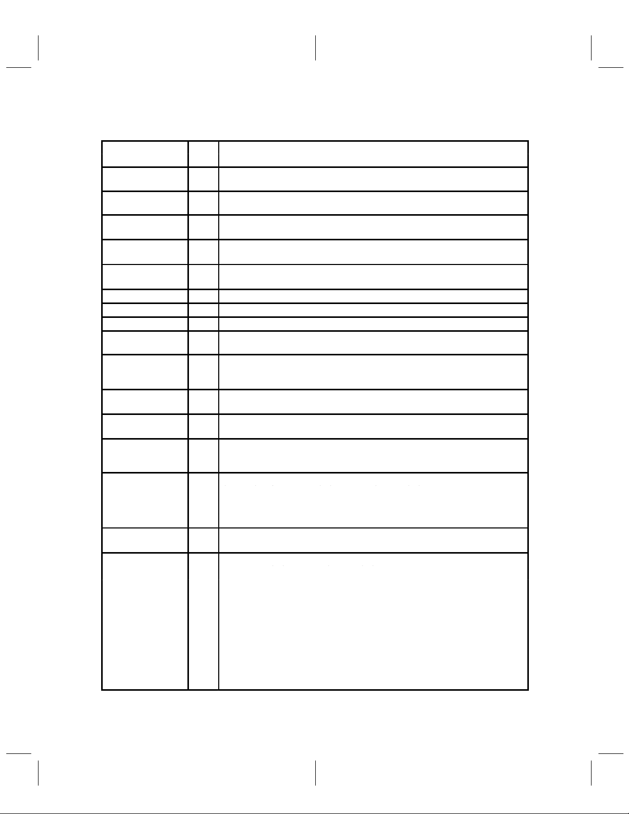
1.4 Terminal Functions
I/O
DESCRIPTION
pgp
pgp
TERMINAL
NAME NO.
AFC 11 O Automatic frequency control. The AFC DAC output provides the means to adjust
AGC 10 O Automatic gain control. The AGC digital-to-analog converter (DAC) output can be
AVDDREF 3 — Analog supply voltage for FM receive path. Power applied to A VDDREF powers the
AVDDRX 7 — Analog supply voltage for receive path. Power applied to AVDDRX powers the receive
AVDDTX 19 — Analog supply voltage for transmit path. Power applied to AVDDTX powers the
AVSSREF 98 — Analog ground for REFCAP
AVSSRX 12 — Analog ground for receive path
AVSSTX 22 — Analog ground for transmit path
BAT 1 I Battery strength monitor. A sample of the battery voltage is applied to BA T, and this
CINT 77 O Controller data interrupt. CINT is the microcontroller data interrupt (active low) signal
CMCLK 92 O Codec master clock. CMCLK provides a 2.048-MHz clock that is used as the master
CSCLK 93 O Codec sample clock. CSCLK provides an 8-kHz frame synchronization pulse for the
DINT 49 O Microcontroller interrupt request. DINT is output when the DSP writes to the SEND
DSPA0 74
DSPA1 73
DSPA2 72
DSPA3 71
DSPCSL 70 I DSP chip select (active low). A low signal at DSPCSL enables the specific DSP
DSPD0 80
DSPD1 81
DSPD2 82
DSPD3 83
DSPD4 84
DSPD5 85
DSPD6 86
DSPD7 87
DSPD8 88
DSPD9 89
†
Z = high impedance
system temperature-compensated reference oscillator (TCXO).
used to control the gain of system receiver circuits.
FM receive path circuitry.
path circuitry.
transmit path circuitry .
sample monitors the battery strength.
that is sent to the DSP. CINT is caused by a microcontroller write to the Send-C
interrupt register location.
clock and bit clock for the speech codec.
speech codec. CSCLK is also connected to the DSP for speech sample interrupts.
DINT register location. DINT can be active high or low according to the levels of the
MTS0 and MTS1 signals.
I DSP 4-bit parallel address bus. DSP A0 through DSP A3 provides the address bus for
the DSP interface. DSPA3 is the MSB, and DSPA0 is the LSB.
addressed.
I/O/Z DSP 10-bit parallel data bus. DSPD0 through DSPD9 provide a 10-bit data bus for the
DSP. DSPD9 is the MSB, and DSPD0 is the LSB.
1–4
Page 13
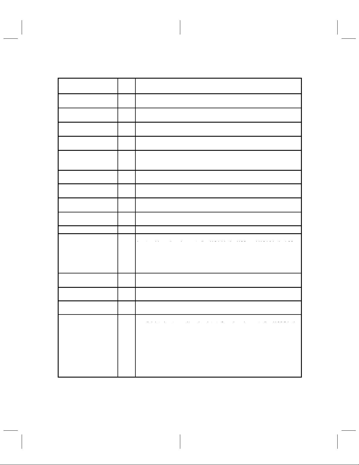
1.4 Terminal Functions (Continued)
I/O
DESCRIPTION
pgp
pgp
MSB
MCD0 is the LSB
TERMINAL
NAME NO.
DSPRW 69 I DSP read/write. A high on DSPRW enables a read operation and a low enables
DSPSTRBL 68 I DSP strobe low . The DSPSTRL (active low) is used in conjunction with DSPCSL
DV
DD
DV
SS
DWBDINT 78 O DSP wide-band data interrupt (active low). The DWBDINT output goes low to
FM 4 I Frequency modulation. FM terminal is connected to the output of the FM
FMRXEN 95 O FM receive path enable. A high output from FMRXEN can be used to enable the
IQRXEN 96 O In-phase and quadrature receive path enable. A high output on IQRXEN can be
LCDCONTR 33 O Liquid-crystal display (LCD) contrast. This LCDCONTR control DAC can be
MCLKOUT 67 O Master clock out. MCLKOUT is a buffered version of MCLKIN.
MCA0 40
MCA1 41
MCA2 42
MCA3 43
MCA4 44
MCCLK 62 O Microcontroller clock. MCCLK provides an adjustable frequency with 1.215 MHz
MCCSH 39 I Microcontroller interface chip-select. A high at MCCSH in conjunction with a low
MCCSL 38 I Microcontroller interface chip-select. A low at MCCSL in conjunction with a high
MCD0 51
MCD1 52
MCD2 53
MCD3 54
MCD4 55
MCD5 56
MCD6 57
MCD7 58
†
Z = high impedance
35, 45, 63,
75, 90
34, 46, 65,
76, 91
a write operation to the DSP.
to enable read/write operations to the DSP.
— Digital power supply. All supply terminals must be connected together.
— Digital ground. All supply terminals must be connected together.
indicate that the wide-band data (WBD) demodulation circuits have traffic on
them.
discriminator.
power for the receiver FM path.
used to enable the power for receiver I/Q path.
used to control the amount of drive to the liquid crystal display.
I Microcontroller 5-bit parallel address bus. MCA0 through MCA4 provide a 5-bit
bus to address the microcontroller. MCA4 is the MSB, and MCA0 is the LSB.
at powerup.
at MCCSL allows the microcontroller to read from or write to the TCM4300.
at the MCCSH allows the microcontroller to read from or write to the TCM4300.
I/O/Z Microcontroller 8-bit parallel data bus. MCD0 through MCD7 provides an 8-bit
parallel data bus to send/receive data to/from the microcontroller. MCD7 is the
, and
.
1–5
Page 14

1.4 Terminal Functions (Continued)
I/O
DESCRIPTION
TERMINAL
NAME NO.
MCDS 48 I Microcontroller data strobe. MCDS is configured by the signals present on MTS0 and
MCLKIN 64 I Master clock input. The MCLKIN frequency input requirement is 38.88 MHz ±100 ppm.
MCRW 47 I Microcontroller read/write. Microcontroller read/write operations are selected in
MTS0 36 I
MTS1 37 I
MWBDFINT 50 O Microcontroller interrupt request. A wide-band data-ready interrupt is output when the
OUT1 26 O Output number 1. OUT1 provides a user-defined general purpose data or control signal.
PAEN 25 O Power amplifier enable. P AEN can be used to enable the transmit power amplifier . This
PWRCONT 16 O Power amplifier (PA) power control. The PWRCONT DAC output can be used to control
RBIAS 99 I Input for bias current-setting resistor. To achieve correct bias voltage, a 100-kΩ, 1%
REFCAP 100 I Reference decoupling capacitor. For proper decoupling, It is recommended that a
RSINL 59 I Reset input low. An active low applied to RSINL resets the TCM4300.
RSSI 2 I Received signal strength indicator. RSSI samples received signal strength.
RSOUTH 60 O Reset out high. An active high is output from RSOUTH for 10 ms after the TCM4300 is
RSOUTL 61 O Reset out low. An active low is output from RSOUTL for 10 ms after the TCM4300 is
RXIN 8 I Negative receive input. The in-phase differential negative baseband received signal is
RXIP 9 I Positive receive input. The in-phase differential positive baseband received signal is
RXQN 5 I Negative receive input. The quadrature negative baseband received signal is applied
RXQP 6 I Positive receive input. The quadrature differential positive baseband received signal is
MTS1.
A crystal can be connected between MCLKIN and XTAL to provide an oscillator circuit.
As an alternative, XTAL can be left open and an external TTL/CMOS-level clock signal
can be connected to MCLKIN.
accordance with the signals present on MTS0 and MTS1.
Microcontroller type select configuration-control inputs. The interface is controlled by
MTS (1:0) as follows:
00 – Intel microcontroller interface characteristics
10 – Mitsubishi and Motorola microcontroller 16-bit bus interface characteristics
01 – Motorola microcontroller 8-bit bus characteristics
11 – Reserved
WBD demodulator is in analog mode or when a frame interrupt is sent by the DSP in
digital mode. MWDBFINT can be active high or low according to the levels of the MTS0
and MTS1 signals.
signal is active high.
the amount of power output from the PA.
tolerance resistor connected between RBIAS and A VSS is recommended.
3.3 µF capacitor in parallel with a 470-pF capacitor be connected between REFCAP and
ground.
powered up.
powered up.
applied to RXIN.
applied to RXIP.
to RXQN.
applied to RXQP.
Intel is a trademark of Intel Corporation.
Mitsubishi is a trademark of Mitsubishi Inc.
Motorola is a trademark of Motorola, Inc.
1–6
Page 15

1.4 Terminal Functions (Continued)
I/O
DESCRIPTION
yg
TERMINAL
NAME NO.
SCEN 94 O Speech CODEC enable. A high out from SCEN can enable the speech CODEC.
SINT 79 O Sample interrupt. SINT is active low. In the analog mode, SINT occurs at 40 kHz; in the
SYNCLK 32 O Synthesizer clock. SYNCLK clocks the serial data stream.
SYNDTA 31 O Synthesizer serial-data. SYNDTA provides the serial bit stream output.
SYNLE0 28 O
SYNLE1 29 O
SYNLE2 30 O
SYNOL 27 I Synthesizer out-of-lock. An active high at SYNOL indicates a synthesizer is not locked.
TXEN 23 O Transmit power enable. An active high output from TXEN can be used to enable various
TXIN 18 O In-phase differential negative baseband transmit. The negative component of the
TXIP 17 O In-phase differential positive baseband transmit. The positive component of the
TXONIND 24 I Transmit on indicator. A signal is applied to TXONIND to indicate that power is applied
TXQN 21 O Quadrature differential negative baseband transmit. The negative component of the
TXQP 20 O Quadrature differential positive baseband transmit. The positive component of the
VCM 15 I Voltage common mode. VCM establishes the dc operating point for transmit outputs and
VHR 14 O Voltage half-rail. The voltage level at VHR is approximately 0.5 × AVDD. VHR
V
SS
XTAL 66 I Crystal input. A crystal connected between XTAL and MCLIN forms an oscillator circuit.
13, 97 — Substrate ground
digital mode, SINT occurs at 48.6 kHz.
Synthesizer 0, 1, and 2 latch enables. An active high on SYNLE0, SYNLE1, and
SYNLE2 indicates that the latch is enabled.
system transmitter-circuit devices.
differential baseband transmit signal is output from TXIN.
differential baseband transmit signal is output from TXIP.
to the power amplifier.
quadrature differential transmit signal is output from TXQN.
quadrature differential transmit signal is output from TXQP.
can be tied to VHR.
establishes the dc operating point for receive inputs.
1–7
Page 16

2 Electrical Specifications
This section lists the electrical specifications, the absolute maximum ratings, the recommended operating
conditions and operating characteristics for the TCM4300 Advanced RF Cellular Telephone Interface
Circuit.
2.1 Absolute Maximum Ratings Over Operating Free-Air Temperature Range
(unless otherwise noted)
Supply voltage range:
DV
(see Notes 1 and 2) VSS –0.3 V to AVDD +0.3 V. . . . . . . . . . . . . . . . . . . . . .
DD
AV
(see Notes 2 and 3) VSS –0.3 V to DVDD +0.3 V. . . . . . . . . . . . . . . . . . . . . . .
Input voltage range, V
Output voltage range, V
Continuous total power dissipation See Dissipation Rating Table. . . . . . . . . . . . . . . . . . .
Operating free-air temperature range, T
Storage temperature range, T
Lead temperature 1,6 mm (1/16 inch) from case for 10 seconds 260°C. . . . . . . . . . . . . .
†
Stresses beyond those listed under “absolute maximum ratings” may cause permanent damage to the device. These
are stress ratings only and functional operation of the device at these or any other conditions beyond those indicated
under “recommended operating conditions” is not implied. Exposure to absolute-maximum-rated conditions for
extended periods may affect device reliability.
NOTES: 1. Voltage values are with respect DVSS.
DD
2. Maximum supplied voltage should not exceed 6 V .
3. Voltage values are with respect to AVSS.
: Digital signals VSS –0.3 V to DVDD +0.3 V. . . . . . . . . . . . . . . . .
I
†
Analog signals V
: Digital signals VSS to DV
O
Analog signals V
–65°C to 150° C. . . . . . . . . . . . . . . . . . . . . . . . . . . . . . . . .
stg
. . . . . . . . . . . . . . . . . . . . . . . . . . .
. . . . . . . . . . . . . . . . . . . . . . . . . . .
–40°C to 85°C. . . . . . . . . . . . . . . . . . . . . . . . . .
A
SS
–0.3 V to AVDD +0.3 V. . . . . . . . . . . . . . . .
to AV
SS
DD
DD
2.2 Dissipation Rating Table
PACKAGE
PZ 1530 mW 15.25 mW/°C 615 mW
TA ≤ 25°C
POWER RATING
DERATING FACTOR
ABOVE TA = 25°C
TA = 85°C
POWER RATING
2–1
Page 17

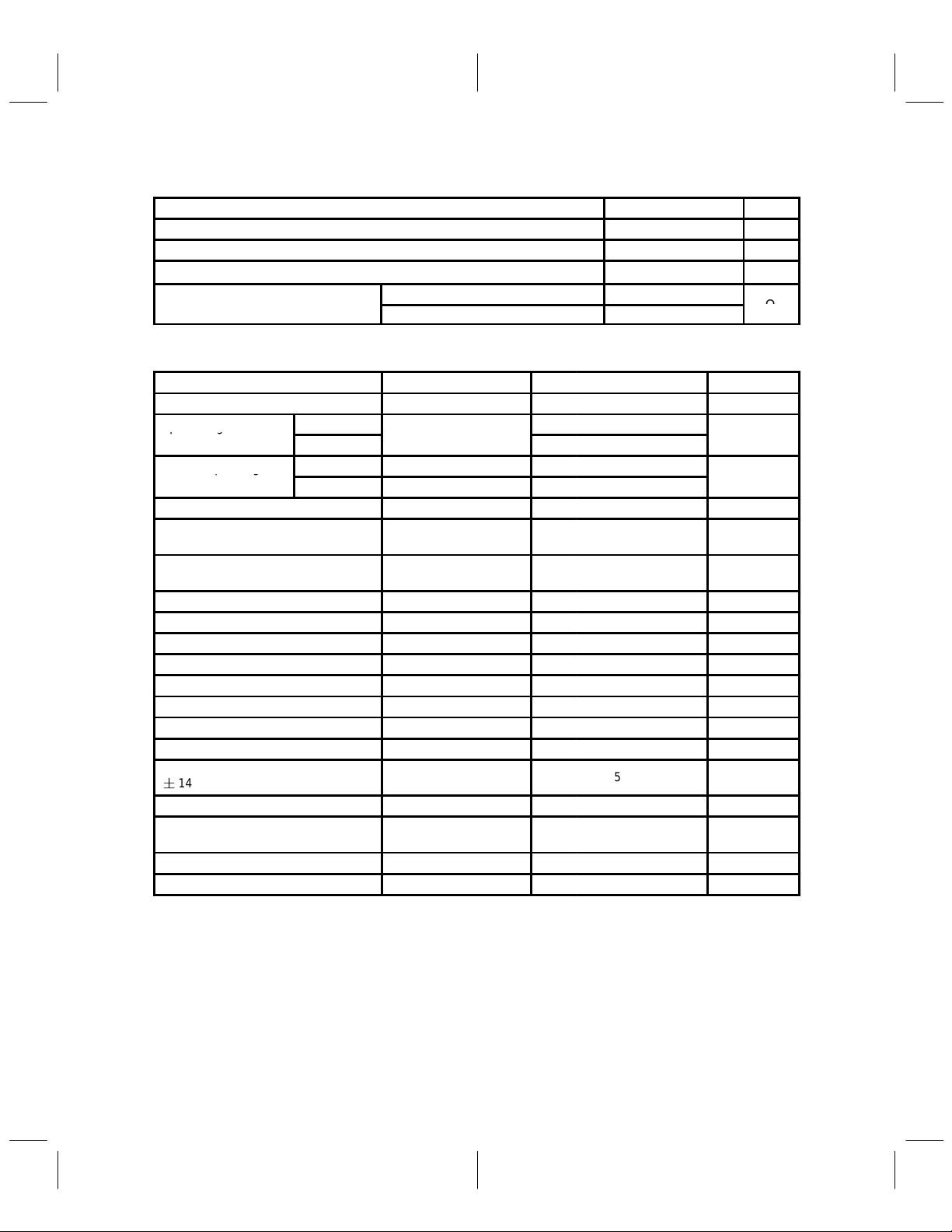
2.3 Recommended Operating Conditions
Anal
itti
W
Digital
W
Digital t
itti
W
Idle mode
mW
g, g g
W
Output
MIN NOM MAX UNIT
Supply voltage, DV
High-level input voltage, V
Low-level input voltage, V
High-level output voltage, V
Low-level output voltage, V
High-level output current at 3 V , I
Low-level output current at 3 V , I
High-level output current at 5 V , I
Low-level output current at 5 V , I
Load capacitance, transmit I and Q channel outputs 50 pF
VCM input voltage range, transmit I and Q channel outputs 1.3 AVDD–1.3 V
Load resistance, auxiliary DACs 10 kΩ
Load capacitance, auxiliary DACs 50 pF
Operating free-air temperature, T
DD
IH
IL
OH
OL
OH
OL
OH
OL
A
Digital 0.7 DV
Digital 0 0.3 DV
Digital 0.7 DV
Digital 0 0.5 V
Digital 2 mA
Digital 2 mA
Digital 2 mA
Digital 2 mA
3 5.5 V
DD
DD
–40 85 °C
DVDD+0.3 V
DD
DV
DD
V
V
2.4 Electrical Characteristics Over Full Range Of Operating Conditions (Unless
Otherwise Noted)
2.4.1 Power Consumption
PARAMETER TEST CONDITIONS MIN TYP†MAX UNIT
og transm
receiving
ransm
Digital mode, 1/3 transmitting +1/3 receiving
+ 1/3 standby
†
All typical values are at TA = 25°C.
ng and receiving
ng
MCLKOUT enabled DVDD = 3 V, AVDD = 3 V 33 40
MCLKOUT disabled DVDD = 3 V, AVDD = 3 V 14 17
MCLKOUT enabled DVDD = 5.5 V, AVDD = 5.5 V 150 160
MCLKOUT disabled DVDD = 5.5 V, AVDD = 5.5 V 80 90
DVDD = 3 V, AVDD = 3 V 65 75
DVDD = 5.5 V, AVDD = 5.5 V 250 275
DVDD = 3 V, AVDD = 3 V 55 60
DVDD = 5.5 V, AVDD = 5.5 V 225 250
DVDD = 3 V, AVDD = 3 V 55 70
DVDD = 5.5 V, AVDD = 5.5 V 210 250
DVDD = 3 V, AVDD = 3 V 50 60
DVDD = 5.5 V, AVDD = 5.5 V 205 220
m
m
m
m
2.4.2 Reference Characteristics
PARAMETER TEST CONDITIONS MIN TYP
V
OH(VHR)
r
O
‡
All typical values are at DVDD = 5 V, AVDD = 5 V, and TA = 25°C
2–2
High-level output voltage 0.5 A VDD–0.2 0.5 AVDD+0.2 V
resistance
FMVOX or IQRXEN
or TXEN = high
FMVOX or IQRXEN
or TXEN = low
‡
MAX UNIT
80 100 Ω
15 40 kΩ
Page 18
2.4.3 T erminal Impedance
MCLKOUT i
Ω
Input voltage for full
V
Nominal operating
‡
FUNCTION MIN TYP†MAX UNIT
Receive channel input impedance (single ended), RXIP/N and RXQP/N 40 70 kΩ
Transmit channel output impedance (single ended), TXIP/N and TXQP/N 40 50 100 Ω
FM input impedance, WBD 25 200 kΩ
mpedance
†
All typical values are at DVDD = 5 V, AVDD = 5 V, and TA = 25°C, unless otherwise specified.
MCLKOUT at 3.3 V 240
MCLKOUT at 5 V 180
2.4.4 RXIP, RXIN, RXQP, and RXQN Inputs (AVDD = 3 V, 4.5 V, 5 V)
PARAMETER TEST CONDITIONS MIN TYP MAX UNIT
Input voltage range 0.3 AVDD–0.3 V
Input voltage for full-
scale digital output
Nominal operating
level
Input CMRR (RXI, RXQ) 45 dB
Sampling frequency , SINT (digital
mode)
Sampling frequency , SINT (analog
mode)
Receive error vector magnitude (EVM) 5% 6%
I/Q sample timing skew Input signal 0 – 15 kHz 50 ns
A/D resolution 10 bits
Signal to noise-plus distortion Input at full scale – 1 dB 54 58 dB
Integral nonlinearity 0 dB to –60 dB input 1 LSB
Gain error (I or Q channel) ±7%
Gain mismatch between I and Q ±0.3 dB
Differential dc offset voltage ±30 mV
FM input sensitivity, full scale
( 14 kHz deviation)
FM input dc offset (relative to VHR) ±80 mV
FM input idle channel noise, below
full-scale input
FM gain error ±6%
Power supply rejection f = 0 kHz to 15 kHz 40 dB
‡
Provides 12 dB headroom for AGC fading conditions.
Differential 0.5
Single ended
Differential 0.125
Single ended 0.125
0.5
48.6 kHz
40 kHz
2.5 Vp-p
–50 dB
p-p
Vp-p
2–3
Page 19

2.4.5 Transmit I and Q Channel Outputs
Peak
VCM
V
Nominal output level (constellation radius) centered
V
pg
PARAMETER MIN TYP MAX UNIT
output voltage full scale, centered at
Nominal output-level (constellation radius) centered
at VCM
Low-level drift ±200 PPM/°C
Transmit error vector magnitude (EVM) 3% 4%
Resolution 8 bits
S/(N+D) ratio at differential outputs 48 52 dB
Gain error (I or Q channel) ±8% ±12%
Gain mismatch between I and Q ±0.3 dB
Gain sampling mismatch between I and Q 20 ns
Zero code error differential ±80 mV
Zero code error, each output, with respect to VCM ±80 mV
Zero code error, I to Q, with respect to other channel (differential or
single ended)
Load impedance, between P and N terminals 10 kΩ
Transmit offset DACs I and Q resolution 6 bits
Transmit offset DACs I and Q average step size 2.9 3.4 3.9 mV
Transmit offset DACs I and Q full-scale positive output 105.4 mV
Transmit offset DACs I and Q full-scale negative output –108.8 mV
Transmit offset DACs differential nonlinearity ±1.1 LSB
Transmit offset DACs integral nonlinearity ±1.1 LSB
Differential 2.24
Single ended 1.12
Differential 1.5
Single ended 0.75
±10 mV
p
2.4.6 Auxiliary D/A Converters
PARAMETER TEST CONDITIONS MIN TYP MAX UNIT
AVDD > 3 V†, AUXFS [1:0] = 00 0.2 2.5
Output range
Resolution AGC, AFC, PWRCONT
DACs
Resolution LCDCONTR DAC 4 bits
Gain + offset error (full scale) AGC,
AFC, PWRCONT DAC
Gain + offset error (full scale)
LCDCONTR DAC
Differential nonlinearity ±0.75 ±1 LSB
Integral nonlinearity ±0.75 ±1 LSB
†
Range settings depends only on AUXFS [1:0]. The supply voltage is not detected.
2–4
AVDD > 4.5 V†, AUXFS [1:0] = 10 0.2 4
AVDD > 5 V†, AUXFS [1:0] = 11 0.2 4.5
8 bits
±3%
±7%
V
Page 20

2.4.7 Auxiliary D/A Converters Slope (AGC, AFC, PWRCONT)
AUXFS[1:0]
SETTING
00 2.5/256 0.0098 1.25 2.5
01 Do not use Do not use Do not use Do not use
10 4/256 0.0156 2 4
11 4.5/256 0.0176 2.25 4.5
†
The maximum input code is 255. The value shown for 256 is extrapolated.
SLOPE
NOMINAL LSB
VALUE
(V)
NOMINAL OUTPUT VOLTAGE
FOR DIGITAL CODE = 128
(MIDRANGE)
(V)
NOMINAL OUTPUT VOLTAGE
FOR DIGITAL CODE = 256†
(MAX VALUE)
(V)
2.4.8 Auxiliary D/A Converters Slope (LCDCONTR)
AUXFS[1:0]
SETTING
00 2.5/16 0.1563 1.25 2.5
01 Do not use Do not use Do not use Do not use
10 4/16 0.2500 2 4
11 4.5/16 0.2813 2.25 4.5
‡
The maximum input code is 15. The value shown for 16 is extrapolated.
SLOPE
NOMINAL LSB
VALUE
(V)
NOMINAL OUTPUT VOLT-
AGE FOR DIGITAL CODE = 8
(MIDRANGE)
(V)
NOMINAL OUTPUT VOLTAGE
FOR DIGITAL CODE = 16
(MAX VALUE)
(V)
2.4.9 RSSI/Battery A/D Converter
PARAMETER TEST CONDITIONS MIN TYP MAX UNIT
Input range AVDD = 3 V, 4.5 V, 5 V 0.2 2 V
Resolution 8 bits
Conversion time AVDD = 3 V, 4.5 V, 5 V 20 µs
Gain + offset error (full scale) ±3% ±4%
Differential nonlinearity ±0.75 ±1 LSB
Integral nonlinearity ±0.75 ±1 LSB
Input resistance 1 2 MΩ
§
2–5
Page 21

2.5 Operating Characteristics Over Full Range of Operating Conditions
qy
dB
qyp
F
dB
(Unless Otherwise Noted)
2.5.1 Receive (RX) Channel Frequency Response (RXI, RXQ Input in Digital Mode)
PARAMETER TEST CONDITIONS MIN TYP MAX UNIT
0.125 V peak-to-peak, 0 kHz to 8 kHz (see Note 4) ±0.5 ±0.75
0.125 V peak-to-peak, 8 kHz to 15 kHz (see Note 5) ±1
Frequency
response
Peak-to-peak
group delay
distortion
Absolute channel
delay, RXI, Q IN to
digital OUT
NOTES: 4. Deviation from ideal 0.35 square-root raised-cosine (SQRC) response
5. Stopband
2.5.2 Receive (RX) Channel Frequency Response (FM Input in Analog Mode)
PARAMETER TEST CONDITIONS MIN TYP MAX UNIT
Frequency response
Peak-to-peak group
delay distortion
Absolute channel delay 2.5 V peak-to-peak, 0 kHz to 6 kHz 400 µs
NOTES: 5. Stopband
6. Ripple magnitude
7. Stopband and multiples of stopband
2.5.3 Transmit (TX) Channel Frequency Response (Digital Mode)
PARAMETER TEST CONDITIONS MIN TYP MAX UNIT
requency response
Peak-to-peak group
delay distortion
Absolute channel delay 0 kHz to 15 kHz 320 µs
NOTES: 4. Deviation from ideal 0.35 square-root raised-cosine (SQRC) response
5. Stopband
0.125 V peak-to-peak, 16.2 kHz to 18 kHz (see Note 5) –26
0.125 V peak-to-peak, 18 kHz to 45 kHz (see Note 5) –30
0.125 V peak-to-peak, 45 kHz to 75 kHz (see Note 5) –46
0.125 V peak-to-peak, > 75 kHz –60
0.125 V peak-to-peak, 0 kHz to 15 kHz 2 µs
0.125 V peak-to-peak, 0 kHz to 15 kHz 325 µs
2.5 V peak-to-peak, 0 kHz to 6 kHz (see Note 6) ±0.5
2.5 V peak-to-peak, 20 kHz to 30 kHz (see Note 5) –18
2.5 V peak-to-peak, 34 kHz to 46 kHz (see Note 7) –48
2.5 V peak-to-peak, 0 kHz to 6 kHz 2 µs
0 kHz to 8 kHz (see Note 4) ±0.3
8 kHz to 15 kHz (see Note 4) ±0.5
20 kHz to 45 kHz (see Note 5) –29
45 kHz to 75 kHz (see Note 5) –55
> 75 kHz (see Note 5) –60
Any 30 kHz band centered at > 90 kHz (see Note 5) –60
0 kHz to 15 kHz 3 µs
dB
2–6
Page 22

2.5.4 Transmit (TX) Channel Frequency Response (Analog Mode)
Frequency response
dB
PARAMETER TEST CONDITIONS MIN TYP MAX UNIT
0 kHz to 8 kHz (see Note 4) ±0.5
8 kHz to 15 kHz (see Note 4) ±0.5
20 kHz to 45 kHz (see Note 5) –31
45 kHz to 75 kHz (see Note 5) –70
> 75 kHz (see Note 5) –70
Any 30 kHz band centered at > 90 kHz (see Note 5) –70
Peak-to-peak group
delay distortion
Absolute channel delay 0 kHz to 15 kHz 540 µs
NOTES: 4. Ripple magnitude
5. Stopband
0 kHz to 15 kHz 3 µs
2–7
Page 23

2–8
Page 24

3 Parameter Measurement Information
This section contains the timing waveforms and parameter values for MCLKOUT and several
microcontroller interface configurations possible when using the TCM4300. The timing parameters are
contained in Section 3.1 through Section 3.11. The timing waveforms are shown in Figures 3–1 through
3–1 1. All parameters shown in the separate waveforms have their values listed in an associated table. Not
all parameter values listed in the tables are necessarily shown in an associated waveform.
3.1 MCLKOUT Timing Requirements (see Figure 3–1 and Note 1)
MIN NOM MAX UNIT
t
t
t
t
NOTE 1: T ested with 15 pF loading on MCLKOUT
Pulse duration , MCLKOUT high 9 10 12 ns
wH
Pulse duration, MCLKOUT low 9 10 12 ns
wL
Rise time, MCLKOUT 2 3 4 ns
r
Fall time, MCLKOUT 2 3 4 ns
f
twH
MCLKOUT
twL
t
r
t
f
V
OH
V
OL
Figure 3–1. MCLKOUT Timing Diagram
3–1
Page 25

3.2 TCM4300 to Microcontroller Interface Timing Requirements (Mitsubishi
Read Cycle) (see Figure 3–2 and Note 2)
PARAMETER
t
su(R/W)
t
h(R/W)
t
su(RA)
t
h(RA)
t
en(RD)
t
v(R)
t
inv
t
dis(RD)
t
h(CS)
t
su(CS)
NOTE 2: Timings are based upon Mitsubishi 37732S4 (16 MHz) and Mitsubishi 3772S4L (8 MHz).
(see Note A)
Setup time, read/write MCRW stable before falling edge of
strobe MCDS
Hold time, read/write MCRW stable after rising edge of
strobe MCDS
Setup time, read address MCS stable before falling edge of
strobe MCDS
Hold time, read address MCA stable after rising edge of
strobe MCDS
Enable time, read data on falling edge of strobe MCDS to
TCM4300 driving data bus MCD
Read data valid time on falling edge of strobe MCDS to
valid data MCD
Data MCD invalid after rising edge of strobe MCDS TRD
Disable time, read data. TCM4300 releases MCD data bus
after rising edge of strobe MCDS
Hold time, chip select MCCSH and MCCSL stable before
rising edge of strobe MCDS
Setup time, chip select MCCSH and MCCSL stable before
falling edge of strobe MCDS
MCDS
MCRW
t
su(R/W)
90%
10%
ALTERNATE
SYMBOL
TRW
(SU)
TRW
(HO)
TRA
(SU)
TRA
(HO)
TRD
(EN)
TRD
(DV)
(INV)
TRD
(DIS)
TCS
(HO)
TCS
(SU)
90%
10%
MIN MAX
0 ns
10 ns
0 ns
10 ns
10 ns
50 ns
10 ns
28 ns
0 ns
0 ns
t
h(R/W)
90%90%
UNIT
t
su(RA)
MCA4–MCA0
t
v(R)
t
en(RD)
MCD7–MCD0
MCCSH
MCCSL
NOTE A: Chip selection is defined as both MCCS and MCDS active.
90% 90%
t
su(CS)
10% 10%
Figure 3–2. Microcontroller Interface Timing Requirements
(Mitsubishi Configuration Read Cycle, MTS [1:0] = 10)
3–2
t
inv
t
h(CS)
t
dis(RD)
t
h(RA)
Page 26

3.3 TCM4300 to Microcontroller Interface Timing Requirements (Mitsubishi
Write Cycle) (see Figure 3–3 and Note 2)
PARAMETER
t
su(R/W)
t
h(R/W)
t
su(WA)
t
h(WA)
t
su(W)
t
h(W)
t
w(WSTB)
t
h(CS)
t
su(CS)
NOTE 2: Timings based upon Mitsubishi 37732S4 (16 MHz) and Mitsubishi 3772S4L (8 MHz).
(see Note A)
Setup time, read/write MCRW stable before falling edge of
strobe MCDS
Hold time, read/write MCRW stable after rising edge of
strobe MCDS
Setup time, write/address MCA stable before falling edge
of strobe MCDS
Hold time, write address MCA stable after rising edge of
strobe MCDS
Setup time, write data stable MCD before rising edge of
strobe MCDS
Hold time, write data stable MCD after rising edge of strobe
MCDS
Pulse duration, write strobe pulse width low on MCDS TWR
Hold time, chip select MCCSH and MCCSL stable before
rising edge of strobe MCDS
Setup time, chip select stable MCCSH and MCCSL before
falling edge of strobe MCDS
t
w(WSTB)
MCDS
t
su(R/W)
90%
10%
ALTERNATE
SYMBOL
TRW
(SU)
TRW
(HO)
TWA
(SU)
TWA
(HO)
TWD
(SU)
TWD
(HO)
(STB)
TCS
(HO)
TCS
(SU)
10%
MIN MAX
0 ns
10 ns
0 ns
10 ns
14 ns
0 ns
60 ns
0 ns
0 ns
90%
t
h(R/W)
UNIT
MCRW
MCA4–MCA0
MCD7–MCD0
MCCSH
MCCSL
NOTE A: Chip selection is defined as both MCCS and MCDS active.
10%
t
su(WA)
t
su(CS)
Figure 3–3. Microcontroller Interface Timing Requirements
(Mitsubishi Configuration Write Cycle, MTS [1:0] = 10)
t
su(W)
t
h(CS)
10%
t
su(WA)
t
h(W)
90%90%
10%10%
3–3
Page 27

3.4 TCM4300 to Microcontroller Interface Timing Requirements (Intel Read
Cycle) (see Figure 3–4 and Note 3)
PARAMETER
t
su(RA)
t
h(RA)
t
en(RD)
t
v(RD)
t
inv
t
dis(RD)
t
su(CS)
t
h(CS)
NOTE 3: Timings are based upon Intel 80C186 (16 MHz).
Setup time, read address MCA stable before falling edge of
strobe MCDS
Hold time, read address MCA stable after rising edge of
strobe MCDS
Enable time, read data on falling edge of strobe MCDS to
TCM4300 driving data bus MCD
Valid time, read data on falling edge of strobe MCDS to
valid data MCD
Data MCD invalid after rising edge of strobe MCDS TRD
Disable time, read data. TCM4300 releases MCD data bus
after rising edge of strobe MCDS
Setup time, chip select MCCSH and MCCSL stable before
falling edge of strobe MCDS
Hold time, chip select MCCSH and MCCSL stable before
rising edge of strobe MCDS
ALTERNATE
SYMBOL
TRA
(SU)
TRA
(HO)
TRD
(EN)
TRD
(DV)
(INV)
TRD
(DIS)
TCS
(SU)
TCS
(HO)
MIN MAX
0 ns
10 ns
10 ns
50 ns
10 ns
28 ns
0 ns
0 ns
UNIT
MCDS
(see Note A)
MCRW
MCA4–MCA0
t
en(RD)
MCD7–MCD0
MCCSH
t
su(CS)
MCCSL
NOTE A: Chip selection is defined as both MCCS and MCDS active.
90% 90%
10% 10%
90%
10%
t
su(RA)
t
v(RD)
Figure 3–4. Microcontroller Interface Timing Requirements
(Intel Configuration Read Cycle, MTS [1:0] = 00)
10%
t
inv
t
h(CS)
90%
t
h(RA)
t
dis(RD)
3–4
Page 28

3.5 TCM4300 to Microcontroller Interface Timing Requirements (Intel Write
Cycle) (see Figure 3–5 and Note 3)
PARAMETER
t
su(WA)
t
h(WA)
t
su(W)
t
h(W)
t
w(WSTB)
t
su(CS)
t
h(CS)
NOTE 3: Timings are based upon Intel 8C186 (16 MHz).
(see Note A)
Setup time, write address MCA stable before falling edge
of strobe MCRW
Hold time, write address MCA stable after rising edge of
strobe MCRW
Setup time, write data stable MCD before rising edge of
strobe MCRW
Hold time, write data stable MCD after rising edge of
strobe MCRW
Pulse duration, write strobe pulse width low on MCRW TWR
Setup time, chip select MCCSH and MCCSL stable before
falling edge of strobe MCRW
Hold time, chip select MCCSH and MCCSL stable before
rising edge of strobe MCRW
MCDS
MCRW
90%
10%
t
su(WA)
t
w(WSTB)
ALTERNATE
SYMBOL
TWA
(SU)
TWA
(HO)
TWD
(SU)
TWD
(HO)
(STB)
TCS
(SU)
TCS
(HO)
10%
MIN MAX
0 ns
10 ns
14 ns
0 ns
60 ns
0 ns
0 ns
90%
t
h(WA)
UNIT
MCA4–MCA0
MCD7–MCD0
MCCSH
t
su(CS)
MCCSL
NOTE A: Chip selection is defined as both MCCS and MCRW active.
Figure 3–5. Microcontroller Interface Timing Requirements
(Intel Configuration Write Cycle, MTS [1:0] = 00)
t
su(W)
t
h(CS)
t
h(W)
90%90%
10%10%
3–5
Page 29

3.6 TCM4300 to Microcontroller Interface Timing Requirements (Motorola
16-Bit Read Cycle) (see Figure 3–6 and Note 4)
PARAMETER
t
su(R/W)
t
h(R/W)
t
su(RA)
t
h(RA)
t
en(RD)
t
v(RD)
t
inv
t
dis(RD)
t
h(CS)
t
su(CS)
NOTE 4: Timings are based upon Motorola 68HC000 (16.67 MHz) and Motorola 68302 (16 MHz).
Setup time, read/write MCRW stable before falling edge of
strobe MCDS
Hold time, read/write MCRW stable after rising edge of
strobe MCDS
Setup time, read address MCA stable before falling edge of
strobe MCDS
Hold time, read address MCA stable after rising edge of
strobe MCDS
Enable time, read data on falling edge of strobe MCDS to
TCM4300 driving data bus MCD
Valid time, read data on falling edge of strobe MCDS to
valid data MCD
Data (MCD) invalid after rising edge of strobe MCDS TRD
Disable time, read data. TCM4300 releases MCD data bus
after rising edge of strobe MCDS
Hold time, chip select MCCSH and MCCSL stable before
falling edge of strobe MCDS
Setup time, chip select stable MCCSH and MCCSL before
rising edge of strobe MCDS
ALTERNATE
SYMBOL
TRW
(SU)
TRW
(HO)
TRA
(SU)
TRA
(HO)
TRD
(EN)
TRD
(DV)
(INV)
TRD
(DIS)
TCS
(HO)
TCS
(SU)
MIN MAX
0 ns
10 ns
0 ns
10 ns
10 ns
50 ns
10 ns
28 ns
0 ns
0 ns
UNIT
MCDS
(see Note A)
MCRW
MCA0–MCA4
MCD0–MCD7
MCCSH
MCCSL
NOTE A: Chip selection is defined as both MCCS and MCDS active.
t
su(R/W)
t
en(RD)
90% 90%
10% 10%
90%
10%
t
t
su(RA)
su(CS)
t
v(RD)
Figure 3–6. Microcontroller Interface Timing Requirements
(Motorola 16-Bit Read Cycle, MTS [1:0] = 10)
3–6
10%
t
inv
t
h(CS)
90%
90%90%
t
h(R/W)
t
t
dis(RD)
h(RA)
Page 30

3.7 TCM4300 to Microcontroller Interface Timing Requirements (Motorola
16-Bit Write Cycle) (see Figure 3–7 and Note 4)
PARAMETER
t
su(R/W)
t
h(R/W)
t
su(WA)
t
h(WA)
t
su(W)
t
h(W)
t
w(WSTB)
t
h(CS)
t
su(CS)
NOTE 4: Timings are based upon Motorola 68HC000 (16.67 MHz) and Motorola 68302 (16 MHz).
(see Note A)
Setup time, read/write MCRW stable before falling edge of
strobe MCDS
Hold time, read/write MCRW stable after rising edge of
strobe MCDS
Setup time, write address MCA stable before falling edge
of strobe MCDS
Hold time, write address MCA stable after rising edge of
strobe MCDS
Setup time, write data stable MCD before rising edge of
strobe MCDS
Hold time, write data stable MCD after rising edge of strobe
MCDS
Pulse duration, write strobe pulse width low on MCDS TWR
Hold time, chip select MCCSH and MCCSL stable before
falling edge of strobe MCDS
Setup time, chip select MCCSH and MCCSL stable before
rising edge of strobe MCDS
t
w(WSTB)
MCDS
t
su(R/W)
90%
10%
ALTERNATE
SYMBOL
TRW
(SU)
TRW
(HO)
TWA
(SU)
TWA
(HO)
TWD
(SU)
TWD
(HO)
(STB)
TCS
(HO)
TCS
(SU)
10%
MIN MAX
0 ns
10 ns
0 ns
10 ns
14 ns
0 ns
60 ns
0 ns
0 ns
90%
t
h(R/W)
UNIT
MCRW
MCA0–MCA4
MCD0–MCD7
MCCSH
MCCSL
NOTE A: Chip selection is defined as both MCCS and MCDS active.
10%
t
su(WA)
t
su(CS)
Figure 3–7. Microcontroller Interface Timing Requirements
(Motorola 16-Bit Write Cycle, MTS [1:0] = 10)
t
su(W)
t
h(CS)
10%
t
h(WA)
t
h(W)
90%90%
10%10%
3–7
Page 31

3.8 TCM4300 to Microcontroller Interface Timing Requirements (Motorola 8-Bit
Ï
Read Cycle) (see Figure 3–8 and Note 5)
PARAMETER
t
su(R/W)
t
h(R/W)
t
su(RA)
t
h(RA)
t
en(RD)
t
v(RD)
t
inv
t
dis(RD)
t
h(CS)
t
su(CS)
NOTE 5: Timings are based upon Motorola 68HC1 1D3 (3 MHz) and Motorola 68HC11G5 (2.1 MHz).
Setup time, read/write MCRW stable before rising edge of
strobe MCDS
Hold time, read/write MCRW stable after falling edge of
strobe MCDS
Setup time, read address MCA stable before rising edge of
strobe MCDS
Hold time, read address MCA stable after falling edge of
strobe MCDS
Enable time, read data on rising edge of strobe MCDS to
TCM4300 driving data bus MCD
Valid time, read data on rising edge of strobe MCDS to valid
data MCD
Data MCD invalid after falling edge of strobe MCDS TRD
Disable time, read data. TCM4300 releases MDS data bus
after falling edge of strobe MCDS
Hold time, chip select MCCSH and MCCSL stable before
falling edge of strobe MCDS
Setup time, chip select MCCSH and MCCSL stable before
rising edge of strobe MCDS
ALTERNATE
SYMBOL
TRW
(SU)
TRW
(HO)
TRA
(SU)
TRA
(HO)
TRD
(EN)
TRD
(DV)
(INV)
TRD
(DIS)
TCS
(HO)
TCS
(SU)
MIN MAX
0 ns
10 ns
0 ns
10 ns
10 ns
50 ns
10 ns
28 ns
0 ns
0 ns
UNIT
MCDS
(see Note A)
t
su(R/W)
MCRW
MCA0–MCA4
MCD0–MCD7
MCCSH
MCCSL
NOTE A: Chip selection is defined as both MCCS and MCDS active.
10%
t
en(RD)
90% 90%
10% 10%
90%
t
t
h(CS)
su(RA)
t
v(RD)
Figure 3–8. Microcontroller Interface Timing Requirements
(Motorola 8-Bit Read Cycle, MTS [1:0] = 01)
3–8
90%
t
inv
t
su(CS)
10%
90%90%
t
h(R/W)
t
t
dis(RD)
h(RA)
Page 32

3.9 TCM4300 to Microcontroller Interface Timing Requirements (Motorola 8-Bit
Write Cycle) (see Figure 3–9 and Note 5)
PARAMETER
t
su(R/W)
t
h(R/W)
t
su(WA)
t
h(WA)
t
su(W)
t
h(W)
t
w(WSTB)
t
h(CS)
t
su(CS)
NOTE 5: Timings are based upon Motorola 68HC1 1D3 (3 MHz) and Motorola 68HC11G5 (2.1 MHz).
(see Note A)
Setup time, read/write MCRW stable before rising edge of
strobe MCDS
Hold time, read/write MCRW stable after falling edge of
strobe MCDS
Setup time, write address MCA stable before rising edge of
strobe MCDS
Hold time, write address MCA stable after falling edge of
strobe MCDS
Setup time, write data stable MCD before falling edge of
strobe MCDS
Hold time, write data stable MCD after falling edge of
strobe MCDS
Pulse duration, write strobe pulse width high on MCDS TWR
Hold time, chip select MCCSH and MCCSL stable before
rising edge of strobe MCDS
Setup time, chip select MCCSH and MCCSL stable before
falling edge of strobe MCDS
t
w(WSTB)
MCDS
t
su(R/W)
10%
90%
ALTERNATE
SYMBOL
TRW
(SU)
TRW
(HO)
TWA
(SU)
TWA
(HO)
TWD
(SU)
TWD
(HO)
(STB)
TCS
(HO)
TCS
(SU)
90%
MIN MAX
0 ns
10 ns
0 ns
10 ns
14 ns
0 ns
60 ns
0 ns
0 ns
10%
t
h(R/W)
UNIT
MCRW
MCA0–MCA4
MCD0–MCD7
MCCSH
MCCSL
NOTE A: Chip selection is defined as both MCCS and MCDS active.
10%
t
su(WA)
t
su(CS)
Figure 3–9. Microcontroller Interface Timing Requirements
(Motorola 8-Bit Write Cycle, MTS [1:0] = 01)
t
su(W)
t
h(CS)
10%
t
h(WA)
t
h(W)
90%90%
10%10%
3–9
Page 33

3.10 Switching Characteristics, TCM4300 to DSP Interface (Read Cycle) (see
Figure 3–10)
ALTERNATE
SYMBOL
TRW
(SU)
TRW
(HO)
TCS
(SU)
TCS
(HO)
TWA
(SU)
TWA
(HO)
TRD
(EN)
TRD
(DV)
TRD
(INV)
TRD
(DIS)
MIN MAX
0 ns
0 ns
0 ns
0 ns
0 ns
0 ns
0 ns
50 ns
5 ns
12 ns
UNIT
t
su(R/W)
t
h(R/W)
t
su(CS)
t
h(CS)
t
su(RA)
t
h(RA)
t
en(R)
t
d(DV)
t
h(R)
t
dis(R)
PARAMETER
Setup time, read/write DSPRW stable before falling edge of
strobe DSPSTRBL
Hold time, read/write DSPRW stable after rising edge of
strobe DSPSTRBL
Setup time, chip select stable DSPCSL before falling edge
of strobe DSPSTRBL
Hold time, chip select DSPCSL stable after rising edge of
strobe DSPSTRBL
Setup time, read address DSPA stable before strobe
DSPSTRBL goes low
Hold time, read address DSPA stable after strobe
DSPSTRBL goes high
Enable time, read data on falling edge of strobe DSPSTRBL
to TCM4300 driving data bus DSPD
Delay read data valid time on falling edge of strobe
DSPSTRBL to valid data DSPD
Hold time, read data DSPD invalid after rising edge of
strobe DSPSTRBL
Disable time, read data. TCM4300 releases data bus after
rising edge of strobe DSPSTRBL
DSPCSL
DSPSTRBL
3–10
DSPRW
DSPA
DSPD
10%
t
su(CS)
90%
10%
t
su(R/W)
90% 90%
t
su(RA)
t
en(R)
t
d(DV)
t
10%
90%
10%
h(R)
Figure 3–10. TCM4300 to DSP Interface (Read Cycle)
t
h(CS)
t
h(R/W)
t
dis(R)
t
h(RA)
Page 34

3.11 Switching Characteristics, TCM4300 to DSP Interface (Write Cycle) (see
Figure 3–11)
ALTERNATE
SYMBOL
TRW
(SU)
TRW
(HO)
TCS
(SU)
TCS
(HO)
TWA
(SU)
TWA
(HO)
TWD
(SU)
TWD
(HO)
(STB)
MIN MAX
0 ns
0 ns
0 ns
0 ns
0 ns
0 ns
3 ns
0 ns
25 ns
UNIT
t
su(R/W)
t
h(R/W)
t
su(CS)
t
h(CS)
t
su(WA)
t
h(WA)
t
su(W)
t
h(W)
t
w(WSTB)
PARAMETER
Setup time, read/write DSPRW stable before falling edge of
strobe DSPSTRBL
Hold time, read/write DSPRW stable after rising edge of
strobe DSPSTRBL
Setup time, chip select stable DSPCSL before falling edge
of strobe DSPSTRBL
Hold time, chip select DSPCSL stable after rising edge of
strobe DSPSTRBL
Setup time, write address DSPA stable before falling edge
of strobe DSPSTRBL
Hold time, write address DSPA stable after rising edge of
strobe DSPSTRBL
Setup time, write data stable DSPD before rising edge of
strobe DSPSTRBL
Hold time, write data stable DSPD after rising edge of
strobe DSPSTRBL
Pulse duration, write strobe pulse width low on DSPSTRBL TWR
DSPCSL
DSPSTRBL
DSPRW
DSPA
DSPD
10%
90%
10%
t
su(CS)
t
su(R/W)
10%
90%
10%
t
su(WA)
t
su(W)
t
w(WSTB)
Figure 3–11. TCM4300 to DSP Interface (Write Cycle)
t
h(CS)
t
h(R/W)
t
h(W)
t
h(WA)
3–11
Page 35

3–12
Page 36

4 Principles of Operation
This section describes the operation of the TCM4300 in detail.
NOTE:
Timing diagrams and associated tables are contained in Section 3 of this data
manual.
4.1 Data Transfer
The interface to both the system digital signal processor and microcontroller is in the form of 2s complement.
4.2 Receive Section
The mode of operation is determined by the state of the MODE, FMVOX, IQRXEN, and FMRXEN bits of
the DStatCtrl register, as shown in Table 4–1.
T able 4–1. TCM4300 Receive Channel Control Signals
CONTROL SIGNAL ANALOG MODE DIGITAL MODE
MODE 0 1
FMVOX 1 0
IQRXEN 0 1
FMRXEN 1 0
In the digital mode (MODE=1), the receive section accepts RXIP, RXIN, RXQP, and RXQN analog inputs.
These inputs are passed to continuous-time antialiasing filters (AAF), baseband filtering, and A/D
conversion blocks, and then to sample registers where 10-bit registers can be read. The sample rate is
48.6 ksps.
In the analog mode (MODE = 0), the FMVOX bit of the DStatCtrl register enables or disables the Q side of
the receiver channel, and the FMRXEN bit controls the external functions. In the digital mode, IQRXEN
enables both the I and Q receive channels and external functions as well.
T o save power, the receive I and Q channels are enabled separately. This operation occurs because in the
analog mode, only the Q channel is used. When the FMVOX bit is set to 1, it controls the input multiplexer ,
connects the FM input to the receiver RXQP signal, and connects the RXQN signal to VHR. When the MODE
control bit and the IQRXEN control bit are set to 1, both sides of the receive channel are enabled for use
in the digital mode.
The input signals RXIP, RXIN and RXQP, RXQN are differential pair signals (see Table 4–2). Differential
signals are used to minimize the pickup of interference, ground, and supply noise, while maintaining a larger
signal level. In single-ended applications, the unused RXIN and RXQN terminals must be connected to VHR
or to an externally supplied bias voltage equal to the dc value of the input signal, and the input signal level
must be adjusted in the RF circuitry to provide the proper signal level so that the digital output codes are
properly calibrated (0.5 V peak-to-peak corresponds to full-scale digital output). In the analog mode, the
RXQN input is internally referenced to VHR. Alternatively, the unused inputs can be connected to VHR and
the used inputs can be capacitively coupled. Note that when the RX and FM inputs are capacitively coupled,
it is recommended that the input terminals be connected to VHR using a bias resistor.
4–1
Page 37
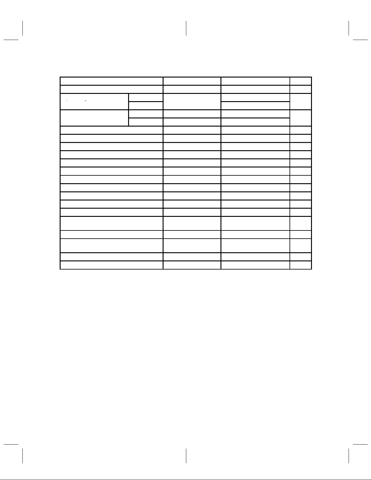
Table 4–2. RXIP, RXIN, RXQP, and RXQN Inputs (AVDD = 3 V, 4.5 V, 5 V)
Input voltage for full scale
V
Nominal
l
†
PARAMETER TEST CONDITIONS MIN TYP MAX UNIT
Input voltage range 0.3 AVDD–0.3 V
Input voltage for full- scale
digital output
operating leve
Input CMRR (RXI, RXQ) 45 dB
Sampling frequency , SINT (digital mode) 48.6 kHz
Sampling frequency , SINT (analog mode) 40 kHz
Receive error vector magnitude (EVM) 5% 6%
I/Q sample timing skew Input signal 0 – 15 kHz 50 ns
A/D resolution 10 Bits
Signal to noise-plus distortion Input at full scale – 1 dB 54 58 dB
Integral nonlinearity 0 dB to –60 dB input 1 LSB
Gain error (I or Q channel) ±7%
Gain mismatch between I and Q ±0.3 dB
Differential dc offset voltage ±30 mV
FM input sensitivity , for full scale (±14 kHz
deviation)
FM input dc offset (wrt VHR) ±80 mV
FM input idle channel noise, below full scale
input
FM gain error ±6%
Power supply rejection f = 0 kHz to 15 kHz 40 dB
†
Provides 12 dB headroom for AGC fading conditions.
Differential 0.5
Single ended
Differential 0.125
Single ended 0.125
0.5
2.5 Vp-p
p-p
Vp-p
–50 dB
It is recommended that the single-ended output of an external FM discriminator be capacitively coupled to
the FM terminal for analog mode voice and WBD reception. An external bias resistor is needed to bias the
FM terminal to VHR. The signal at this terminal is conveyed to the Q side of the receiver using the multiplexer,
and the other Q input is connected internally to the VHR reference voltage. The I input of the receive section
circuitry is disabled in the analog mode. The FM signal passes through the antialiasing filter, as specified
in T able 4–3, before passing through the A/D converter. The signal at the FM terminal is also routed directly
to the WBD demodulator through a low-pass filter (LPF) with the –3 dB point at 270 kHz.
4–2
Page 38

T able 4–3. Receive (RX) Channel Frequency Response (FM Input in Analog Mode)
qyp
pp
qy
0.125 V
k
dB
PARAMETER TEST CONDITIONS MIN TYP MAX UNIT
0 kHz to 6 kHz (see Note 1) ±0.5
Frequency response 2.5 V peak-to-peak
Peak-to-peak group
delay distortion
Absolute channel delay 2.5 V peak-to-peak, 0 kHz to 6 kHz 400 µs
NOTES: 1. Ripple magnitude
2. Stopband
3. Stopband and multiples of stopband
2.5 V peak-to-peak, 0 kHz to 6 kHz 2 µs
20 kHz to 30 kHz (see Note 2) –18
34 kHz to 46 kHz (see Note 3) –48
dB
The VHR can provide a bias voltage for the received inputs when capacitively coupled from the RF section.
To meet noise requirements, the VHR output should have an external decoupling capacitor connected to
ground. The VHR output buffer is enabled by the OR of TXEN, FMVOX, and IQRXEN. The VHR output is
high impedance otherwise.
In the digital mode, both the I and Q receive sides are enabled. T able 4–4 lists the receive channel frequency
response.
Table 4–4. Receive (RX) Channel Frequency Response (RXI, RXQ Input in Digital Mode)
PARAMETER TEST CONDITIONS MIN TYP MAX UNIT
0 kHz to 8 kHz (see Note 4) ±0.5 ±0.75
8 kHz to 15 kHz (see Note 4) ±1
Frequency
response
Peak-to-peak
group delay
distortion
Absolute channel
delay, RXI, Q IN to
digital OUT
NOTES: 2. Stopband
4. Deviation from ideal 0.35 square-root raised-cosine (SQRC) response.
peak-to-pea
0.125 V peak-to-peak, 0 kHz to 15 kHz 2 µs
0.125 V peak-to-peak, 0 kHz to 15 kHz 325 µs
16.2 kHz to 18 kHz (see Note 2) –26
18 kHz to 45 kHz (see Note 2) –30
45 kHz to 75 kHz (see Note 2) –46
> 75 kHz –60
When the I and Q sample conversion is complete and the data is placed in the RXI and RXQ sample
registers, the SINT interrupt line is asserted to indicate the presence of that data. This occurs at 48.6-kHz
rate in the digital mode and at 40-kHz rate in the analog mode. In the analog mode, only the RXQ conversion
path is used, and the RXI path is powered down.
4.3 Transmit Section
The transmit section operates in two distinct modes, digital or analog. The mode of operation is determined
by the MODE bit of the DStatCtrl register. In the digital mode, data is input to the transmit section by writing
to the TXI register. The resulting output is a π/4 DQPSK-modulated time division multiplexed (TDM) burst.
In the analog mode, the data is in the form of direct I and Q samples which are written to both the TXI and
TXQ registers, then D/A converted, filtered, and output through TXIP, TXIN, TXQP, and TXQN. The I and
Q outputs are zero-IF FM signals; that is, no baseband connection is necessary for FM transmission.
In the digital mode (MODE = 1), the data is written to the TXI register using the SINT interrupt to synchronize
the data transfer. The TCM4300 performs parallel-to-serial conversion of the bits in the TXI register and
encodes the resulting bit stream as π/4 DQPSK data samples. These samples are then filtered by a digital
4–3
Page 39

square-root raised-cosine (SQRC) shaping filter with a roll-off rate of α = 0.35 and converted to sampled
Peak
VCM
V
Nominal output level (constellation radius) centered at
V
analog form by two 9-bit digital-to-analog converters (DACs). The output of the DAC is then filtered by a
continuous-time resistance-capacitance (RC) filter.
The TCM4300 generates a power amplifier (P A) control signal, PAEN, to enable the power supply for the
PA. The start and stop times of the TDM burst are controlled by writing to a single bit, TXGO, in the DSP
DStatCtrl register.
In the analog mode (MODE = 0), the DSP writes 8-bit I and Q samples into the TXI and TXQ data registers
at a 40-ksps rate. These writes are timed by the SINT interrupt signal. The samples are fed to a low-pass
filter before D/A conversion. In the transmit analog mode, PAEN is always set to 1.
The transmit section provides differential I and Q outputs (see T able 4-5) for both analog and digital modes.
The differential dc offset for the TXI and TXQ outputs can be independently adjusted using the transmit offset
registers.
Table 4–5. Transmit (TX) I and Q Channel Outputs
PARAMETER MIN TYP MAX UNIT
output voltage full scale, centered at
Nominal output-level (constellation radius) centered at
VCM
Low-level drift ±200 PPM/°C
Transmit error vector magnitude (EVM) 3% 4%
Resolution 8 bits
S/(N+D) ratio at differential outputs 48 52 dB
Gain error (I or Q channel) ±8% ±12%
Gain mismatch between I and Q ±0.3 dB
Gain sampling mismatch between I and Q 20 ns
Zero code error differential ±80 mV
Zero code error, each output, with respect to VCM ±80 mV
Zero code error, I to Q, with respect to other channel (differential or
single ended)
Load impedance, between P and N terminals 10 kΩ
Transmit offset DACs I and Q resolution 6 bits
Transmit offset DACs I and Q average step size 2.9 3.4 3.9 mV
Transmit offset DACs I and Q full-scale positive output 105.4 mV
Transmit offset DACs I and Q full-scale negative output –108.8 mV
Transmit offset DACs differential nonlinearity ±1.1 LSB
Transmit offset DACs integral nonlinearity ±1.1 LSB
Differential 2.24
Single ended 1.12
Differential 1.5
Single ended 0.75
p
±10 mV
Modulation Error: In the digital mode, during the transmit burst, the complex output of the transmitter circuits
consists of an ideal output s = I
magnitude (EVM) is defined as the peak value of the magnitude of e relative to the ideal output:
Modulation error percentage+100
T able 4–6 and Table 4–7 show the frequency response of the transmit section for digital and analog mode,
respectively.
4–4
ideal
+ jQ
+ error e = ei + jeq. In Table 4-5, the modulation error vector
ideal
|e|
%
|s|
Page 40

T able 4–6. Transmit (TX) Channel Frequency Response (Digital Mode)
F
dB
Frequency response
dB
PARAMETER TEST CONDITIONS MIN TYP MAX UNIT
0 kHz to 8 kHz (see Note 4) ±0.3
8 kHz to 15 kHz (see Note 4) ±0.5
requency response
Peak-to-peak group
delay distortion
Absolute channel delay 0 kHz to 15 kHz 320 µs
NOTES: 2. Stopband
4. Deviation from ideal 0.35 SQRC response
20 kHz to 45 kHz (see Note 2) –29
45 kHz to 75 kHz (see Note 2) –55
> 75 kHz (see Note 2) –60
Any 30 kHz band centered at > 90 kHz (see Note 2) –60
0 kHz to 15 kHz 3 µs
T able 4–7. Transmit (TX) Channel Frequency Response (Analog Mode)
PARAMETER TEST CONDITIONS MIN TYP MAX UNIT
0 kHz to 8 kHz (see Note 1) ±0.5
8 kHz to 15 kHz (see Note 1) ±0.5
20 kHz to 45 kHz (see Note 2) –31
45 kHz to 75 kHz (see Note 2) –70
> 75 kHz (see Note 2) –70
Any 30 kHz band centered at > 90 kHz (see Note 2) –70
Peak-to-peak group
delay distortion
Absolute channel delay 0 kHz to 15 kHz 540 µs
NOTES: 1. Ripple magnitude
2. Stopband
0 kHz to 15 kHz 3 µs
4.4 Transmit Burst Operation (Digital Mode)
In the digital mode, the TCM4300 performs all encoding, signal processing, and power ramping for the burst.
Start and stop timing of the variable length bursts are set by means of the TXGO bit in the DStatCtrl
register. The SINT interrupt output interrupts the DSP at 48.6 kHz which is T/2 interval (T = 1 symbol
period = 1/24.3 kHz). The burst is initiated by the DSP writing 1 to 5 dibits to the TXI register, a small
positive-delay offset value d to the base station (BST) register, and a 1 to the TXGO bit in the DStatCtrl
register.
The TXGO bit is sampled on the falling edge of SINT. The transmit outputs are held at zero differential
voltage (each output terminal is held at the voltage supplied to the VCM input terminal) for 9.5 SINT periods
(195.5 µs) plus BST offset delay after SINT has detected TXGO high; then the transmit outputs begin to ramp
to the initial π/4 DQPSK constellation value. The shape of the ramp is the transient resulting from the internal
SQRC filtering. At the same time that the transmit outputs are beginning to ramp, the PAEN digital output
goes high. This output can enable the power amplifier of a cellular radio transmitter. The TCM4300 transmit
outputs reach the first π /4 DQPSK constellation value (maximum effect point, MEP) 6 SINT periods (3
symbol periods) after the start of the ramp.
The bit stream to be encoded as π/4 DQPSK symbols is generated by right shifts on each SINT of the TXI
register with bit 0 (LSB) used first.
Previously written data continues to propagate through the TCM4300 internal filters until the last π/4 DQPSK
constellation value (last MEP) occurs at the transmit outputs 15.5 SINT periods (318.9 µs) plus BST offset
4–5
Page 41

delay after the last symbol occurs (2 SINT periods before TXGO goes low); then the transmit outputs decay
to zero differential voltage (each output at the voltage supplied to the VCM input terminal). The shape of the
decay is the transient resulting from the internal SQRC filtering. The transmit outputs are held at zero
differential voltage 6 SINT periods (3 symbol periods) after the start of the decay . At this time the PAEN digital
output is set low (see Figure 4–1 and Figure 4–2).
Nonzero values of the BST offset register increase the delays of both the transmit waveforms and PAEN
relative to the edges of TXGO after it is internally sampled by SINT . The delays are increased in increments
of 1/4 SINT (1/8 symbol period).
For delays of 1 SINT or greater, the fractional part of the delay can be achieved using the BST of fset register
with the remaining integer SINT delay implemented externally by delaying the writing to TXGO and TXI.
The relative timing of P AEN and the transmit waveforms is not affected by the BST offset register.
The IS-54 standard describes shortened bursts and normal bursts. The two types differ in duration and
number of transmitted bursts, burst length being determined by the TXGO bit.
N+3 SINT Periods
(N = Total number of bits sent)
9.5 SINT Periods
†
SINT
TXGO
TXI data bit
PAEN
TXI/Q output ramp
Input Bits
Dibit transmission
†
Total delay = d (SINT/4 or T/8) where d = integer value (0,1,2,3) written to the BST offset register.
d(T/8)
6 SINT Periods
>>> >>>
>>>
First MEP Last MEP
15.5 SINT Periods +d(T/8)
19.5 SINT Periods +d(T/8)
>>>
4–6
Figure 4–1. Power Ramp-Up/Ramp-Down TIming Diagram
Page 42

Dibit
In
DQ
BST Offset
Delay
Channel Delay
(15.5 SINT Periods)
TXI,
TXQ
TXGO
SINT
CLK
DQ
CLK
Delay = 0, 1/4, 1/2, 3/4
BST Offset
Delay
SYNOL
MPAEN
Transmit Channel Delay + d(T/8)
Occurs from last symbol (2 SINT periods)
before TXGO goes low
PAEN Delay
9.5
19.5
PAEN Delay + d(T/8)
TXGO high: 9.5 SINT periods + d(T/8): PAEN high
TXGO low: 19.5 SINT periods + d(T/8): PAEN low
PAEN
Figure 4–2. Transmit Power Ramp-Up/Ramp-Down Functional Diagram
4.5 Transmit I And Q Output Level
In the digital mode, the output level at TXI and TXQ is controlled by the TCM4300. During the burst, but not
including ramp-up or ramp-down periods, the average output level (I
specified value. There is no variable level control for TXI and TXQ within the TCM4300 other than the fixed
ramping. In the analog mode, the output of the TCM4300 depends only on the sample values written to the
TXI and TXQ registers.
There are small differences in the average output power levels between the digital and the analog modes.
These differences require compensation at the system level by a small attenuation in the sample values of
the analog output.
2
+ Q2)
1/2
should approximate the
When a change in transmit power is necessary, the microcontroller can change the value sent to the
PWRCONT DAC, the output of which can be connected to a voltage-controlled attenuator in the transmit
path of the RF section.
4.6 Wide-Band Data Demodulator
The wide-band data demodulator (WBDD) module demodulates the FM signal and outputs a
Manchester-decoded data stream. The WBDD is used for receiving the analog control channels of the
forward control channel (FOCC) and the forward voice channel (FVC). The bit error rate (BER) performance
requirements are listed in Table 4–8.
4–7
Page 43

Table 4–8. Typical Bit-Error-Rate Performance (WBD_BW = 000)
PARAMETER
MIN
MAX
UNIT
TEST CONDITIONS
MEAN CNR
Bit error rate
–5
0
5
10
15
20
25
0.4
0.279
0.143
0.056
0.0192
0.00623
0.00199
dB
The WBDD is controlled by the bits in the control register WBDCtrl (see Table 4–9).
Table 4–9. Bits in Control Register WBDCtrl
NAME BIT CODE FUNCTION
WBD_LCKD — Indicates whether edge detector is locked (1) or unlocked (0)
WBD_ON — Turns the WBDD module on/off (1/0)
WBD_BW
000 20 Hz
001 39 Hz
010 78 Hz
011 156 Hz
100 313 Hz
101 625 Hz
110 1250 Hz
Sets the appropriate PLL bandwidth
WBD_LCKD: This bit reduces the effects of signal dropouts due to fading. In the Manchester-coded signal,
there are two types of data edges. One type occurs at the midpoint of each data bit, and the other occurs
randomly, depending on the transmitted data sequence. Inside the WBDD, an edge detector rapidly
synchronizes itself to the midpoint edges when the WBD_LCKD bit clears to 0. However, when a signal
dropout occurs, the edge detector may momentarily lock to the wrong edge because it cannot distinguish
the midpoint edges from the data edges. A small number of additional bits may be lost in this instance.
When the WBD_LCKD bit is set to 1, the edge detector uses the WBDD internal phase lock loop (PLL) output
to distinguish the correct edge. Once acquisition of data has occurred, when this bit is set to 1, the loss of
bits due to signal dropouts is restricted to the fade duration only .
When the WBDD PLL is not synchronized, as at power up, the WBD_LCKD bit must be cleared to 0 to allow
edge synchronization to the data.
WBD_BW: The variable bandwidth is required for fast acquisition in the beginning using a wide bandwidth
for the PLL, and a narrower bandwidth is used afterwards to reduce the likelihood of noise causing loss of
synchronization.
The WBDCtrl register is accessible by both the DSP and the microcontroller.
4.7 Wide-band Data Interrupts
The WBDD operates whenever WBD_ON is high, and it does not require the receive channels to be
enabled. While WBD_ON is high, every 800 µs, 8 bits are placed in the WBD register, which is accessible
by both the DSP and the microcontroller ports. This value should be written at the same time as WBD_ON
is initially set high.
4–8
Page 44

At the same time, the interrupts DWBDINT and MWBDFINT are asserted. The interrupt rate is 800 µs
(8 bits/10 kHz). These interrupts are individually cleared when the WBD register is read by the
corresponding processor. They can also be cleared by their respective processor by writing a 1 to the
corresponding clear WBD bit.
There is one WBD control register. It can be written to by either processor port.
4.8 Wide-band Data Demodulator General Information
The WBDD recovers the transmitter clock from the data stream, which is Manchester encoded, and decodes
the data bits. Consideration at the system level is required to ensure data integrity .
The WBD stream carries with it a 10-kHz clock. The Manchester-coded data format contains a transition
at the middle of every bit-clock period, which aids in clock recovery. The polarity of the transition is
data-dependent. In a typical Manchester-coded WBD stream, a positive voltage for the first half of the data
sequence bit time followed by a negative voltage for the second half of the data sequence bit time represents
the value 0 in the data sequence. Likewise, a negative voltage followed by a transition to a positive voltage
represents the value 1 in the data sequence. This is illustrated in Figure 4–3. The WBD stream can also be
seen as the exclusive-OR of the clock and data sequence. The data sequence is in nonreturn to zero (NRZ)
format.
Data
Sequence
WBD
Stream
Recovered Clock
10 kHz
011 0010
Figure 4–3. WBD Manchester-Coded Data Stream
4–9
Page 45

4.9 Auxiliary DACs, LCD Contrast Converter
pg
Auxiliary DACs generate AFC, AGC and power control signals for the RF system. These three D/A
converters are updated when the corresponding data is received from the DSP . In fewer than 5 µs after the
corresponding registers are written to, the output has settled to within 1 LSB of its new value (see
Table 4–10).
Table 4–10. Auxiliary D/A Converters
PARAMETER TEST CONDITIONS MIN TYP MAX UNIT
AVDD > 3 V†, AUXFS [1:0] = 00 0.2 2.5
Output range
Resolution AGC, AFC, PWRCONT
DACs
Resolution LCDCONTR DAC 4 bits
Gain + offset error (full scale) AGC,
AFC, PWRCONT DAC
Gain + offset error (full scale)
LCDCONTR DAC
Differential nonlinearity ±0.75 ±1 LSB
Integral nonlinearity ±0.75 ±1 LSB
†
Range settings depends only on AUXFS [1:0]. The supply voltage is not detected.
AVDD > 4.5 V†, AUXFS [1:0] = 10 0.2 4
AVDD > 5 V†, AUXFS [1:0] = 11 0.2 4.5
8 bits
±3%
±7%
The LCDCONTR output is used by the microcontroller to adjust the contrast of the liquid-crystal display
(LCD). This converter is a separate 4-bit DAC.
The auxiliary DACs can be powered down. The AGC and AFC DACs have dedicated bits in the MIntCtrl
register to enable the DACs. The PWRCONT DAC is enabled by the TXEN bit in the DStatCtrl register. The
LCDCONTR DAC is enabled when the LCDEN bit of the LCD D/A register clears to 0, the four data bits being
left justified. The AFC, AGC, and PWRCONT DACs are disabled after powerup or after a reset of the
TCM4300. After power up or reset, the default AUXFS[1:0] is 00. When the DACs are powered down, their
output terminals go to a high-impedance state and can tolerate any voltage present on the terminal that falls
within the supply range.
The slope and the corresponding output values for the auxiliary DACs are listed in Table 4–11 and
Table 4–12.
Table 4–11. Auxiliary D/A Converters Slope (AGC, AFC, PWRCONT)
AUXFS[1:0]
SETTING
00 2.5/256 0.0098 1.25 2.5
01 Do not use Do not use Do not use Do not use
10 4/256 0.0156 2 4
11 4.5/256 0.0176 2.25 4.5
‡
The maximum input code is 255. The value shown for 256 is extrapolated.
SLOPE
NOMINAL LSB
VALUE
(V)
NOMINAL OUTPUT VOLTAGE
FOR DIGITAL CODE = 128
(MIDRANGE)
(V)
NOMINAL OUTPUT VOLTAGE
FOR DIGITAL CODE = 256
(MAX VALUE)
(V)
V
‡
4–10
Page 46

4.9 Auxiliary DACs, LCD Contrast Converter (continued)
Table 4–12. Auxiliary D/A Converters Slope (LCDCONTR)
AUXFS[1:0]
SETTING
00 2.5/16 0.1563 1.25 2.5
01 Do not use Do not use Do not use Do not use
10 4/16 0.2500 2 4
11 4.5/16 0.2813 2.25 4.5
†
The maximum input code is 15. The value shown for 16 is extrapolated.
SLOPE
NOMINAL LSB
VALUE
(V)
NOMINAL OUTPUT VOLT-
AGE FOR DIGITAL CODE = 8
(MIDRANGE)
(V)
NOMINAL OUTPUT VOLTAGE
FOR DIGITAL CODE = 16†
(MAX VALUE)
(V)
4.10 RSSI, Battery Monitor
The received signal strength indicator (RSSI) and battery (BA T) strength monitor share a common register.
The input source is determined by writing any value to the mapped register location for that analog-to-digital
converter (ADC) (see T able 4–13), and the result of the conversion is stored in both register locations. The
conversion process is initiated when the register is written to. The CVRDY bit in the MStatCtrl register is set
to 1 to show completion of the conversion process. Reading from either of the register locations causes the
CVRDY bit to change to 0. The RSSI allows the mobile unit to choose the proper control channels and to
report signal levels to the base stations.
When the CVRDY bit in the MStatCtrl register goes to 1, this indicates that the latest RSSI or battery voltage
A/D conversion has been completed and can be read from the RSSI or BA T register location. CVRDY clears
to 0 when the microcontroller reads either of these locations.
Table 4–13. RSSI/Battery A/D Converter
PARAMETER TEST CONDITIONS MIN TYP MAX UNIT
Input range AVDD = 3 V, 4.5 V, 5 V 0.2 2 V
Resolution 8 bits
Conversion time AVDD = 3 V, 4.5 V, 5 V 20 µs
Gain + offset error (full scale) ±3% ±4%
Differential nonlinearity ±0.75 ±1 LSB
Integral nonlinearity ±0.75 ±1 LSB
Input resistance 1 2 MΩ
In order to save power, the entire RSSI/battery converter circuit is powered down when no A/D conversions
are requested for 40 µs. The microcontroller writes to RSSI or BA T registers, causing power to be applied
to the converter circuit. Power is applied to the converter circuit until the data value has been latched into
the corresponding register, at which time power to the converter is removed. Data remains in the result
registers after the converter is powered down.
4.11 Timing And Clock Generation
The digital timing generation system uses a 38.88-MHz master clock as shown in Figure 4–4. The upper
waveform shows the clock generation for clocks that must be phase adjusted in order to synchronize the
mobile unit with the received symbol stream in the digital mode. In the analog mode, these clocks operate
without phase adjustments. The bottom waveform of Figure 4–4 shows the clocks that are directly derived
from the master clock.
4–11
Page 47

Codec Master Clock 2.048 MHz
CMCLK
Codec Sample Clock 8 kHz
CSCLK
Figure 4–4. Codec Master and Sample Clock Timing
4.11.1 Clock Generation
There are three options for generating the master clock. A fundamental crystal or a third-overtone crystal
with a frequency of 38.88 MHz can be connected between the MCLKIN and the XTAL terminals or an
external clock source can be connected directly to the MCLKIN terminal. The MCLKOUT is a buffered
master clock output at the same frequency as MCLKIN. MCLKOUT can be used as the source clock for other
devices in the system. Setting the MCLKEN bit in the MStatCtrl register enables or disables this output. The
MCLKOUT enable is synchronous with MCLKIN to eliminate abnormal cycles of the clock output.
All output clocks are derived from the master clock (MCLKIN). The sample clocks for the digital and analog
modes, the 8-kHz speech codec sample clock, and the clocks for the A/D and D/A functions are also derived
from the master clock.
4.11.2 Speech-Codec Clock Generation
The TCM4300 generates two clock outputs for use with speech codecs: the 2.048-MHz CMCLK and the
8-kHz CSCLK. These clocks are generated so that each CSCLK period contains exactly 256 cycles of
CMCLK. Since 2.048 MHz is not an integer division of the 38.88-MHz MCLKIN, one out of every 64 CMCLK
cycles is 18 MCLKIN periods long, and the remaining 63 out of 64 are 19 MCLKIN periods long. The average
frequency of MCLKIN is therefore
63
ǒ
MCLKIN
CSCLK is exactly CMCLK divided by 256 (see Figure 4–4).
To save power, the codec clocks are only generated by TCM4300 when the SCEN bit of the DStatCtrl
register is set high. When SCEN is low, both outputs, CSCLK and CMCLK, are held low. SCEN is also
available as an output.
19
)
64
18
1
Ǔ
+
2.048092 MHz
4.11.3 Microcontroller Clock
A variable modulus divider provides a selection of frequencies for use as a microcontroller clock. The master
clock is divided by an integer from 32 to 2, giving a wide range of frequencies available to the microcontroller
(1.215 MHz to 19.88 MHz). The modulus can be changed by writing to the microcontroller clock register.
The output duty cycle is within the requirements of most microcontrollers, that is, from 40% to 60%. At
power-on reset, the clock divider defaults to 1.215 MHz.
4.11.4 Sample Interrupt SINT
The SINT interrupt signal is the primary timing signal for the TCM4300 interface. The primary function of
the SINT is to indicate the ready condition to receive or transmit data. It also conveys timing marks to allow
for the synchronization of system DSP functions. In the digital mode, SINT is used in conjunction with the
received sync word to track cellular system timing. The SINT can be disabled by writing a 1 to the SDIS bit
of the DIntCtrl register. When enabled, the SINT operates continuously at 48.6 kHz in the digital mode and
at 40 kHz in the analog mode. The SINT signal does not require an interrupt acknowledge. The SINT is active
low for 5.5 MCLK cycles (141.5 ns) in the analog mode and 6.5 MCLK cycles (167.2 ns) in the digital mode.
4–12
Page 48

4.11.5 Phase-Adjustment Strategy
For an IS-54 system in the digital mode, receiver sample timing must be phase adjusted to synchronize the
A/D conversions to optimum sampling points of the received symbols, and to synchronize the mobile unit
timing to the base station timing. This is done by temporarily increasing or decreasing the periods of the
clocks to be adjusted. T o avoid undesirable transients, each cycle of the clock being adjusted is altered by
only one period of MCLKIN. A total adjustment equivalent to multiple MCLKIN periods is accomplished by
altering multiple cycles of the clock being adjusted. The number of cycles altered is controlled by internal
counters.
In the TCM4300 there are two clocks which must be adjusted: CMCLK and an internal 9.72-MHz clock from
which SINT is derived. Each of these clocks has an associated counter that counts the number of cycles
that have been lengthened or shortened by one MCLKIN period each and thus detects when the total
adjustment is complete. These counters are shown in Figure 4–5 as Adjust Counter A and Adjust Counter B.
The magnitude of the 2s complement value written to the timing adjustment register determines the number
of cycles of the clocks to be lengthened or shortened by one MCLKIN period each to achieve the total desired
timing adjustment in units of MCLKIN periods. If a negative number is written, the clock periods are
lengthened for the duration of the timing adjustment, resulting in a timing delay. If a positive number is
written, the clock periods are shortened for the duration of the timing adjustment, resulting in a timing
advance.
The divider generates CMCLK normally divides MCLKIN by either 19 or 18. When the CMCLK period is
being lengthened during a timing adjustment, MCLKIN is divided by either 20 or 19. When the CMCLK period
is being shortened, MCLKIN is divided by either 18 or 17 (see subsection 4.11.2). The divider used to
generate a 9.72-MHz clock divides by 4 during normal operation, by 5 when its period is being lengthened
during timing adjustments, and by 3 when its period is being shortened during timing adjustments.
Because CMCLK and the 9.72-MHz internal clock have different periods, and the timing adjustments are
limited to one period of MCLKIN per period of the clock, these clocks take different times to complete the
entire timing adjustment. Because the total adjustment is the same number of MCLKIN periods for both
clocks, the relative phases of the two clocks are the same after the adjustment as they were before.
Both adjust counters reach zero when the adjustment is complete, so there is no need to write to the timing
adjustment register until another timing adjustment is required. For each write to the timing adjustment
register, a single timing adjustment of the direction and magnitude requested is performed.
The output of each adjustment counter is fed to a variable modulus divider. For counter A, there are three
possible moduli, 3, 4, and 5. For counter B there are four possible moduli, 17, 18, 19, and 20.
4–13
Page 49

From DSP
38.88 MHz
MCLKIN
From
Micro-
controller
÷ 17, 18, 19, 20
Adjust
Counter B
10
Adjust
Counter A
÷ 3, 4, 5
Analog/Digital
Mode (MODE bit)
5
÷ N
Divider
N = (2, 3, . . . 32)
MCLKEN
= 0 ÷ 256
Bits 0–5
Phase-Adjusted
9.72-MHz Clock
÷ 243/
÷ 200
Clock
Chain
Sync.
Enable
Logic
2.048-MHz Codec Master Clock CMCLK
RCO
8-kHz Codec Sample Clock CSCLK
40.0/48.6-kHz A/D Sample Clock (SINT)
Frequency Synth. Clock 303.75 kHz
WBD Demod. 6.48 MHz
Microcontroller Clock MCCLK
External Clock Output MCLKOUT
Analog/Digital
ADC Clocks
DAC Clocks
4–14
Figure 4–5. Timing and Clock Generation for 38.88-MHz Clock
Page 50

4.12 Frequency Synthesizer Interface
The synthesizer interface provides a means of programming three synthesizers. The synthesizer-side
outputs are a data line, a clock line, and three latch enable lines that separately strobe data into each
synthesizer. The control inputs are registers mapped into the microcontroller address space. The status of
the interface can be monitored to determine when the programming operation has been completed.
The synthesizer interface is designed to be general purpose. Most of the currently available synthesizers
can be accommodated by programming the interface according to the required synthesizer data and logic
level formats.
The output of the synthesizer interface consists of five signals. SYNCLK is the common data clock for all
attached synthesizer chips. The clock rate is MCLK/128 (≈304 kHz). The clock pulse has a 50% duty factor.
The serial data output SYNDTA is common to all synthesizers. Three strobe signals, SYNLE0, SYNLE1,
and SYNLE2, are provided. There is one for each synthesizer chip. The attributes of this interface are
controlled by means of the synthesizer control registers, SynCtrl0, SynCtrl1, and SynCtrl2. These attributes
determine:
• The polarity of the clock (rising or falling edge)
• Whether data is shifted left or right
• The number of bits sent to the synthesizer
• The timing and polarity of the latch enable bits
• The selection of which synthesizer to program
Programming of the synthesizers is accomplished by writing to four microcontroller-mapped data registers.
These registers are chained to form a 32-bit data shift register that can be operated in either shift left or shift
right mode. This register set can accommodate various formats of synthesizer control data. When fewer
than 32 bits of data are to be transmitted, the significant data bits must be justified such that the first bit to
be transferred is either the LSB or the MSB of the register set, as defined by the control register for LSB or
MSB first operation. All 32 bits of the data register are transmitted each time (see Section 4.15 for register
location and Figure 4–6 for a representative block diagram of the frequency synthesizer interface).
4–15
Page 51

SYNDTA
Ready
and
Timing Logic
CLKPOL
NUMCLKS
LOWVAL
HIGHVAL
SEL[2:0]
MSB/LSB FIRST
SYNRDY To MStatCtrl Register
5
5
5
3
Control
Registers
SYNLE0
SYNLE1
SYNLE2
SYNCLK
D
Q
E
SEL 0
D
Q
A = B
A = B
B ≤ A
A
B
A
B
A
B
HIGHVAL
LOWVAL
NUMCLKS
SEL 1
E
S
D
Q
SEL 2
E
Clock
Circuit
Q
R
CLKPOL
Figure 4–6. Synthesizer Interface Circuit Block Diagram
M
U
X
32
5
5
BIT CNT
[0 . . . 31]
32-Bit Data
Register
DMUX
8
µC
Bus
MSB/LSB
FIRST
303.75 KHz
4–16
Page 52

The SynData0 register contains the least significant bits of the 32-bit data register . SynData3 contains the
SynCtrl0
SynCtrl2
most significant bits. The bits in the SynCtrl0, SynCtrl1, and SynCtrl2 registers are allocated as shown in
Figure 4–7.
7–5 4–0
SEL[2:0] LOWVAL
7–6 5 4–0
SynCtrl1
Reserved
7–6 5 4–0
Reserved CLKPOL NUMCLKS
MSB/LSB
FIRST
HIGHVAL
Figure 4–7. Contents of SynData Registers
Table 4–14 identifies the meaning of each of the bit fields in SynCtrl[2:0].
Table 4–14. Synthesizer Control Fields
NAME DESCRIPTION
CLKPOL This is a 1-bit field. When CLKPOL = 1, the SYNCLK signal is a positive-going, 50% duty cycle
NUMCLKS This 5-bit field defines the total number of clock pulses that are to be produced on SYNCLK. The
HIGHVAL This 5-bit field defines when the strobe signal for the selected synthesizer is driven high. HIGHV AL
LOWVAL The value written into this 5-bit field affects the strobe signal for the selected synthesizer. LOWV AL
MSB/LSB FIRST Writing a 0 to MSB/LSB FIRST causes the LSB (SynData0[0]) to be the first bit sent to SYNDTA
SEL[2:0] This is a 3 bit field that selects which synthesizer strobe line is active. A 1 in any of the SELx bits
pulse. CLKPOL = 0 reverses the polarity of SYNCLK.
value written into NUMCLKS is the desired number of output clock pulses, with one exception:
When 32 clock pulses are desired, all zeroes are written into NUMCLKS.
is the bit number at which the signal changes state. Bits being transferred on SYNDTA are
sequentially designated 0, 1, ... 31, independent of any MSB/LSB selection.
is the bit number at which the strobe signal is driven low. The first bit transferred out of the serial
interface is defined to occur at bit-time 0, independent of any MSB/LSB selection.
of the serial synthesizer interface. Writing a 1 to this bit programs the block for MSB first operation,
SynData3[7].
activates the corresponding latch enable.
In the status register MStatCtrl, two bits, SYNOL and SYNRDY , are dedicated to the synthesizers. The first
is an out-of-lock indicator that comes from the SYNOL input terminal. When the SYNOL input terminal is
connected to the OR of the out-of-lock signals from the external synthesizers, the lock condition of the
synthesizers can be monitored by reading the MStatCtrl register. A high on SYNOL also prevents the P AEN
output from being asserted and forces the TXI and TXQ outputs to zero. The SYNRDY bit, active high,
indicates when the synthesizer interface is idle and ready for programming. When SYNRDY is low, the
synthesizer interface is busy.
Controlling the synthesizer interface is straightforward. The microcontroller checks to see if the SYNRDY
bit is low. When it is low , the synthesizer interface is not ready. When SYNRDY goes high, the microcontroller
programs the desired information into the four registers. When the microcontroller write to the SynCtrl2
register is complete, the synthesizer interface sets the SYNRDY bit low and begins to send data, clock, and
latch enable according to the format established in the registers. SYNRDY returns high when the entire
operation is complete.
4–17
Page 53

Up to 31 data bits plus a latch enable (SYNLE0,1,2) can be programmed in one programming cycle. When
data greater than or equal to 32 bits must be programmed, TI recommends using two or more programming
cycles with data in each cycle and a latch enable in the final programming cycle. Two or more programming
cycles are recommended because all programming cycles must contain at least one SYNCLK pulse,
whereas the latch enable can be suppressed in any programming cycle.
Figure 4–8 shows an example of the synthesizer output signals. In this case, an 18-bit pattern, 0x10664,
was chosen to write into synthesizer 1 with a positive-going latch enable pulse at the eighteenth bit. In order
to do so, the microcontroller writes the values 00h into SynData0, 00h into SynData1, 99h into SynData2,
41h into SynData3, 52h into SynCtrl0, 31h into SynCtrl1, and 32h into SynCtrl2.
SYNCLK
SYNDTA
10 6 6 4
SYNLE1
SYNLE0, 2
SYNRDY
Figure 4–8. Example Synthesizer Output
4.13 Power Control Port
For systems requiring minimum system current consumption, power can be provided to each functional part
of the TCM4300 only when that function is required for proper system operation. To accomplish this, the
TCM4300 provides six external power control signals accessible through the DStatCtrl and MStatCtrl
registers. These signals can be used to minimize the on time of the functional units. These power control
signals are SCEN, FMRXEN, IQRXEN, TXEN, P AEN, and OUT1 (see Table 4–15). The polarity of each of
these signals is high enable, low disable.
T able 4-15. External Power Control Signals
NAME SUGGESTED EXTERNAL APPLICATION
SCEN Speech codec (microphone/speaker interface circuit) enable 0
FMRXEN FM demodulator enable 0
IQRXEN I and Q receive enable. IQRXEN enables the QPSK demodulator and the AGC amplifier 0
TXEN Transmit enable. TXEN enables power to the transmitter signal processing circuits: QPSK
modulator, voltage-controlled amplifier, driver amplifier , PA negative bias. This signal can
be used to enable these subsystems only during the transmit burst in digital mode.
OUT1 User defined 0
PAEN Power amplifier enable. PAEN enables power to P A. 0
4–18
RESET
VALUE
0
Page 54
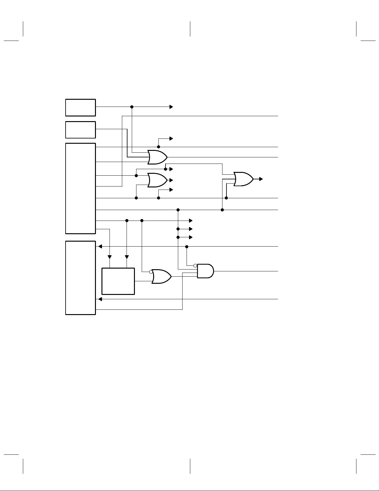
In addition to allowing control of power to external functional modules, these power control bits combined
e
with other control bits are used to control internal TCM4300 functions. This control system is shown in
Figure 4–9.
WBD
Ctrl
MIntCtrl
DStatCtrl
MStatCtrl
WBD_ON
FMRXEN
SCEN
FMRXEN
FMVOX
OUT1
IQRXEN
TXEN
MODE
TXGO
Transmitter
Control
Circuits
WBD Demodulator Circuit
SC Clock Generation
Q-Side Input MUX
Q-Side RX Enable
I-Side RX Enable
TX and RX Filter Select
TX Signal Processing
PWRCONT, Enable (Hi-z when disabled)
OUT1
SCEN
FMRXEN
VHR High Drive Enabl
(Hi-Z when disabled)
IQRXEN
TXEN
SYNOL
PAEN
TXONIND
MPAEN
Figure 4–9. Internal and External Power Control Logic
T o allow for further system power savings, the TCM4300 receive I and Q channels are enabled separately
because only the Q side is used in analog mode. The FMVOX bit controls the Q-side input multiplexer. When
FMVOX is high, the QP side of the receiver is connected to the FM input terminal, the QN input is connected
to the VHR reference voltage, and the Q side of the receiver is powered up. The MODE bit controls the
Q-side filter characteristics for digital or analog mode. The IQRXEN bit enables both the I and Q receiver
sides. The bit IQRXEN can be set high while still in analog mode (FMVOX high or MODE low) to allow
sufficient power-up settling time for the external receiver I and Q circuits.
Setting the MODE bit low connects RXQP to the FM input and RXQN to VHR.
In the digital mode (MODE bit set high), setting IQRXEN high turns on both sides of the receiver. The TXEN
enables the internal transmit functions. When the TXEN bit is set low, the PWRCONT output goes to a
high-impedance state and the P AEN output is set low. The TXEN signal can be used to power down most
of the external transmit circuits between transmit bursts.
4–19
Page 55

In the analog mode, (MODE bit set low), PAEN is high whenever TXEN is active and SYNOL is low. The
SYNOL input can be used as an indication to the TCM4300 that the external synthesizers are out of lock.
The P AEN signal is gated by SYNOL to prevent off-channel transmissions.
The TXEN, IQRXEN, FMVOX, and MODE signals are generated by sampling the corresponding bits of the
DStatCtrl register with the internal SINT . The effect of a write to the DStatCtrl register on these signals does
not appear until the next SINT after the write.
4.14 Microcontroller-DSP Communications
The microcontroller and the DSP communicate by means of two separate 32-byte first-in first-out (FIFO)
buffers. Figure 4–10 illustrates this scheme. The microcontroller writes to FIFO A, but data read from the
same address comes from FIFO B. On the DSP side, the situation is reversed.
Send CINT,
CINT Status,
Clear DINT
CINT
DSP
µC
DINT
FIFO A
8
8
FIFO B
Send DINT,
DINT Status,
Clear CINT
Figure 4–10. Microcontroller-DSP Data Buffers
To send data to the DSP, the microcontroller writes data to FIFO A. To indicate to the DSP that FIFO A is
ready to be read, the microcontroller writes a 1 to the Send-C bit of the microcontroller interrupt control
register MIntCtrl. When this happens, the DSP interrupt line CINT goes active, signaling to the DSP that data
is waiting. At the same time, the value that can be read from the Clear-C bit in the DIntCtrl register goes from
0 to 1, indicating that the interrupt is pending. When the DSP writes a 1 to the Clear-C bit, the CINT line
returns to the inactive state and the value that can be read from Clear-C is 0. The microcontroller cannot
deassert the CINT line.
The microcontroller-DSP communications interface is symmetric. Data sent from the DSP to the
microcontroller is handled as described above, with the roles of A and B FIFOs and C and D bits and
interrupts reversed. When the number of reads exceeds the number of writes from the other side, the values
read are undefined.
4–20
Page 56
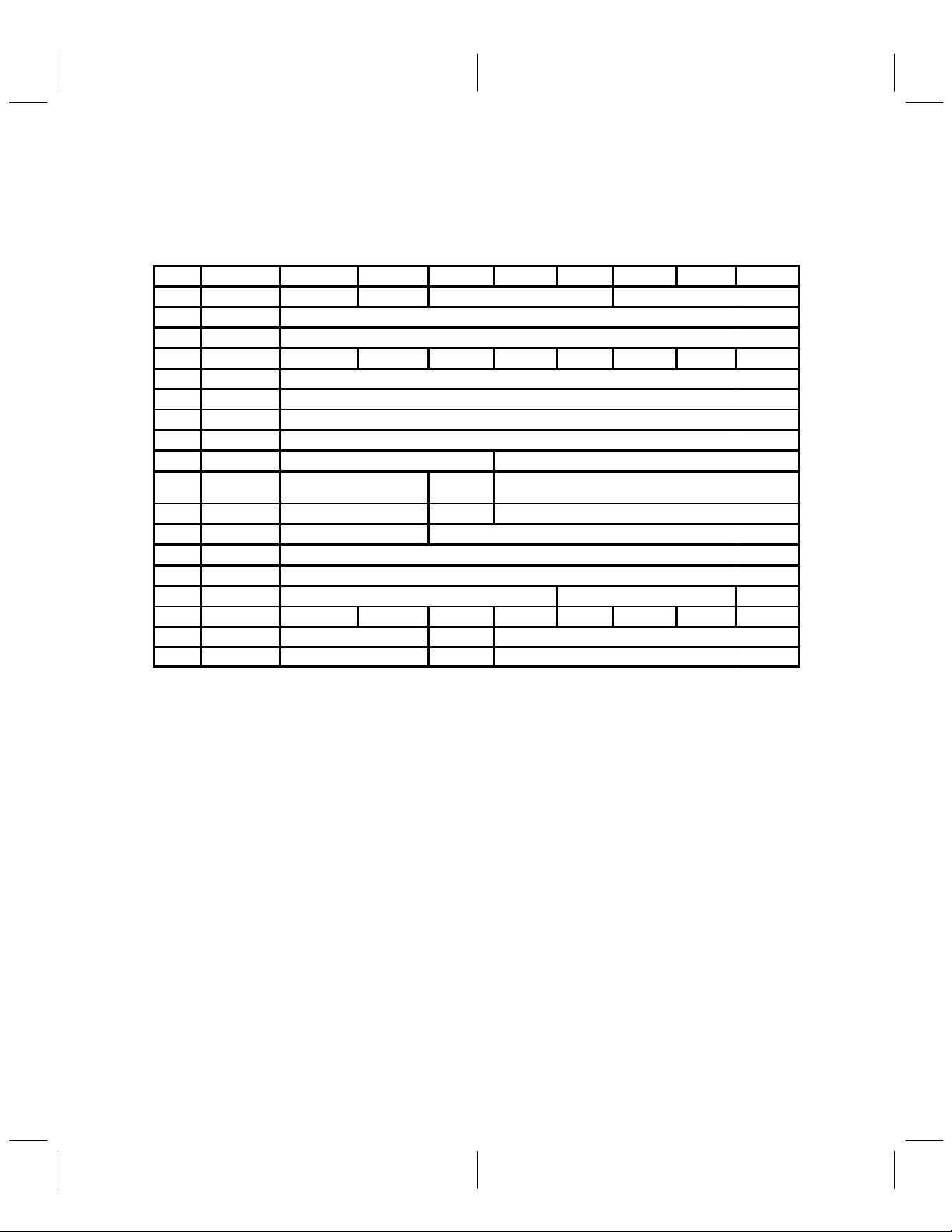
4.15 Microcontroller Register Map
The microcontroller can access 17 locations within the TCM4300. The register locations are 8 bits wide as
shown in Table 4–16 and Table 4–17.
T able 4–16. Microcontroller Register Map
ADDR NAME D7 D6 D5 D4 D3 D2 D1 D0
00h WBDCtrl WBD_LCKD WBD_ON WBD_BW Reserved
00h WBD MSB LSB
01h FIFO MSB FIFO A(B) Microcontroller to DSP (DSP to microcontroller) LSB
02h MIntCtrl Clear WBD Clear-F Clear-D Send-C AGCEN AFCEN
03h SynData0 MSB LSB
04h SynData1 MSB LSB
05h SynData2 MSB LSB
06h SynData3 MSB LSB
07h SynCtrl0 SEL[2:0] LOWVAL
08h SynCtrl1 Reserved
09h SynCtrl2 Reserved CLKPOL NUMCLKS
0Ah MCClock Reserved MSB LSB
0Bh RSSI A/D MSB LSB
0Ch BAT A/D MSB LSB
0Dh LCD D/A MSB LSD Reserved LCDEN
0Eh MStatCtrl SYNOL TXONIND SYNRDY MCLKEN CVRDY AuxFS1 AuxFS0 MPAEN
0Fh TXI Offset Reserved Sign MSB LSB
10h TXQ Offset Reserved Sign MSB LSB
MSB/LSB
FIRST
HIGHVAL
FMRXEN
Reserved
4–21
Page 57

T able 4–17. Microcontroller Register Definitions
Wide-band dat
y
T
ADDR NAME CATEGORY R/W
00h WBDCtrl
00h WBD
01h FIFO FIFO A(B) microcontroller to DSP (DSP to microcontroller) W/(R)
02h MIntCtrl Interrupt/control status R/W
03h SynData0
04h SynData1
05h SynData2
06h SynData3
07h SynCtrl0
08h SynCtrl1 W
09h SynCtrl2 W
0Ah MCClock Microcontroller clock speed W
0Bh RSSI A/D RSSI level R
0Ch BAT A/D Battery level monitor R
0Dh LCD D/A LCD contrast control W
0Eh MStatCtrl Miscellaneous status/control R/W
0Fh TXI Offset
10h TXQ Offset
Synthesizer interface
ransmit dc offset compensation
a
W
R
W
W
W
W
W
W
W
4.16 Wide-Band Data/Control Register
This register is used for two functions, depending on whether it is being read from or written to. When read
from, the register provides the latest 8 bits of received and demodulated data according to the
microcontroller register map to the microcontroller. When it is written to, the bits are placed into the WBDCtrl
register (see Table 4–16) as shown here:
7 6 5–3 2–0
WBDCtrl WBD_LCKD WBD_ON WBD_BW[2:0] Reserved
W W W
When the WBDCtrl register is read, bit 7 (MSB) is the last received data bit.
The definition of the WBDCtrl register, according to the DSP register map, is shown in Table 4–18.
4–22
Page 58

T able 4–18. WBDCtrl Register
BIT R/W NAME FUNCTION RESET VALUE
9 R/W WBD_LCKD
8 R/W WBD_ON Wide-band data on. WBD_ON turns the WBDD module on/off (1/0). 0
7–5 R/W WBD_BW[2:0] Wide-band data bandwidth. WBD_BW[2:0] sets the appropriate
4–0 — — Reserved —
Wide-band data lock data. WBD_LCKD determines whether edge
detector is locked (1) or unlocked (0).
PLL bandwidth.
000 : 20 Hz
001 : 39 Hz
010 : 78 Hz
011 : 156 Hz
100 : 313 Hz
101 : 625 Hz
110 : 1250 Hz
0
110
4.17 Microcontroller Status and Control Registers
MCClock: This location is used by the microcontroller to change the speed of its own clock. The division
modulus is equal to a binary coded value written into this register. Only bits [5:0] are significant. After reset,
MCClock is equal to MCLKIN/32. Division moduli 2 through 32 are valid (0-1 moduli are prohibited). The
clock speed change occurs after the write is complete.
MIntCtrl Bits [7:4]: The bit names in this field indicate the resulting action when the bit is set to 1. When these
bits are being read, a 1 indicates that the corresponding interrupt is pending. A 0 indicates that the interrupt
is clear. W riting a 0 into any bit location has no effect.
MIntCtrl Bits [3:1]: These bits enable power to the AGC and AFC DACs and their corresponding outputs as
shown below. FMRXEN can assert (set to 1) the FMRXEN external function. The reset value is 0 (off).
7 6 5 4 3 2 1 0
MIntCtrl
Clear
WBD
R/W R/W R/W R/W R/W R/W R/W
Clear-F Clear-D Send-C AGCEN AFCEN FMRXEN Reserved
MStatCtrl: This register contains various signals needed for system monitoring and control as shown here
(also see Table 4–19).
7 6 5 4 3 2 1 0
MStatCtrl
SYNOL TXONIND SYNRDY MCLKEN CVRDY AuxFS1 AuxFS0 MPAEN
R R R R/W R R/W R/W R/W
4–23
Page 59

Table 4–19. MStatCtrl Register Bits
R/W
PWRCONT and also LCD CONTR DAC. The microcontroller selects
()
BIT R/W NAME FUNCTION RESET VALUE
Synthesizer out of lock. SYNOL is equal to the level applied to SYNOL
7 R SYNOL
6 R TXONIND
5 R SYNRDY
4 R/W MCLKEN
3 R CVRDY
2
1
0 R/W MPAEN
AuxFS[1]
AuxFS[0]
input pin. SYNOL can be used as an input for an externally generated
status signal to prevent transmission when external synthesizers are
out of lock. In digital mode, when SYNOL is high, PAEN is not asserted
and no signal can be transmitted from TXIP, TXIN, TXQP, and TXQN.
Transmitter on indicator. TXONIND is equal to the level applied to
TXONIND, and it can indicate that power is applied to the power
amplifier.
Synthesizer interface ready. SYNRDY indicates that frequency
synthesizer is ready to be programmed by the microcontroller. When
SYNRDY is 1, the microcontroller can program the frequency
synthesizer interface; a 0 indicates the interface circuit is busy.
MCLKOUT enable. When MCLKEN is set to 1 by the microcontroller,
the 38.88-MHz master clock is output at MCLKOUT. Writing 0 to
MCLKEN disables MCLKOUT.
Conversion ready. A 1 indicates that the latest RSSI or battery voltage
A/D conversion is complete and can be read from the RSSI or battery
register location. CVRDY goes to 0 when the microcontroller reads from
either of these locations.
Auxiliary DACs full-scale select. The auxiliary DACs are AGC, AFC,
PWRCONT and also LCD CONTR DAC. The microcontroller selects
the full-scale output ranges with these bits (see Table 4–11 and
Table 4–12 for bit-to-output range mapping).
Microcontroller P A enable. A 0 indicates that the external PA enable line
PAEN is prevented from going active (see Figure 4–9).
Level on
SYNOL input
terminals
Level for
TXONIND input
terminals
1
1
1
0
0
0
TXI Offset and TXQ Offset: These registers allow the differential offset voltages TXIP – TXIN and
TXQP – TXQN to be adjusted to compensate for internal and/or external offsets. The magnitude of
adjustment is D × step size, where D is a 6-bit, 2s-complement integer written into bits 5–0 of these registers,
as shown here:
7–6 5–0
TXI(Q) Offset
Reserved TXI(Q) Offset Value
W
4.18 LCD Contrast
The LCD contrast register allows for 16 levels of control of terminal LCD contrast. The register is input to
the LCD contrast D/A converter allowing control of the level of intensity of the LCD display as shown here:
7–4 3–1 0
LCDEN
(active low)
4–24
LDC D/A
LCD Contrast Reserved
W W
Page 60

4.19 DSP Register Map
RX ch
A/D
R
04h
TXI
W
05h
TXQ
W
The register map accessible to the DSP port is shown in Table 4–20 and Table 4–21. There are 14 system
addressable locations. Note that the write address of FIFO B is the same as the read address of FIFO A.
Figure 4-1 1 details the connection of TCM4300 to an example DSP.
Table 4–20. DSP Register Map
ADDR NAME D9 D8 D7 D6 D5 D4 D3 D2 D1 D0
00h WBD MSB LSB Reserved
01h WBDCtrl WBD_LCKD WBD_ON WBD_BW Reserved
02h RXI Sign MSB LSB
03h RXQ Sign MSB LSB
04h TXI Sign MSB LSB
05h TXQ Sign MSB LSB
06h FIFO MSB FIFO A(B) microcontroller to DSP (DSP to microcontroller) LSB Reserved
07h DlntCtrl Clear WBD SDIS Clear-C Send-D Send-F Reserved
08h Timing Adj MSB LSB
09h AGC DAC MSB LSB Reserved
0Ah AFC DAC MSB LSB Reserved
0Bh PWR DAC MSB LSB Reserved
0Ch DStatCtrl TXGO MODE SCEN FMVOX FMRXEN IQRXEN TXEN OUT1 RXOF ALB
0Dh BST Offset Reserved MSB LSB
T able 4–21. DSP Register Definitions
ADDR NAME CATEGORY R/W
00h WBD Wide-band data R
01h WBDCtrl Wide-band data control R/W
02h RXI
03h RXQ
06h FIFO FIFO A(B) microcontroller to DSP (DSP to microcontroller) R/(W)
07h DIntCtrl Interrupt control/status R/W
08h Timing Adj Symbol timing adjust W
09h AGC DAC AGC W
0Ah AFC DAC AFC W
0Bh PWR DAC Power control W
0Ch DStatCtrl Miscellaneous status/control R/W
0Dh BST Offset TDM burst offset W
annel
Analog mode: TXI D/A data
Digital mode: π/4 DQPSK modulator input data
Analog mode: TXQ D/A data
Digital mode: Not used
results
4–25
Page 61

DSPD[9:0]
DSPA[3:0]
10
D[15:6]
4
A[3:0]
DSPCSL
DSPRW
DSPSTRBL
SINT
CINT
BDINT
IS
R/W
STRB
INT 1
INT 3
INT 4
DSPTCM4300
Figure 4–11. DSP Interface
4.20 Wide-Band Data Registers
Bit 9 of the wide-band data register is the most recently received bit as shown below.
9–2 1–0
WBD
WBDCtrl
9 8 7–5 4–0
WBD_LCKD WBD_ON WBD_BW Reserved
WB Data Reserved
R
R/W
4.21 Base Station Offset Register
BST OFFSET values are 00, 01, 10, and 11, which correspond to an offset value d of 0, 1, 2, and 3
respectively as shown below.
9–2 1–0
BST OFFSET
Reserved Offset[1:0]
The delay in the TCM4300 TX channels is increased by the amount:
T
BST OFFSET
4–26
+
d
SINT
4
W
Page 62

4.22 DSP Status and Control Registers
DIntCtrl, Clear and Send Bits: The bit names in the DIntCtrl register indicate the action to be taken when
a 1 is written to the respective bit. When these bits are being read, a 1 indicates that the corresponding
interrupt is pending. A 0 indicates that the interrupt is not pending. Writing a 0 to any bit has no effect. Writing
a 1 to the clear bits clears the corresponding interrupt, and the interrupt terminal returns to its inactive level.
Writing a 1 to the send bits causes the corresponding interrupt to go active.
DIntCtrl, SDIS: When a 1 is written to the SDIS bit, the SINT interrupt going to the DSP is disabled. The
disabling and re-enabling function is buffered to prevent the SINT signal from having shortened periods of
output active. The SDIS bit is active (1) upon reset.
9 8 7 6 5 4–0
DlntCtrl
The DStatCtrl register contains various signals needed for system monitoring and control. These are
described in Table 4–22.
DStatCtrl
BIT R/W NAME FUNCTION
9 R/W TXGO
8 R/W MODE
7 R/W SCEN
6 R/W FMVOX
5 R/W FMRXEN FM receiver enable. FMRXEN is connected to bit 5 (see Figure 4–9). 0
4 R/W IQRXEN
3 R/W TXEN
2 W OUT1 Output 1. OUT1 is a user-defined general purpose data or control signal. 0
1 R/W RXOF
0 R/W ALB
Clear WBD SDIS Clear-C Send-D Send-F Reserved
R/W
9 8 7 6 5 4 3 2 1 0
TXGO MODE SCEN FMVOX FMRXEN IQRXEN TXEN OUT1 RXOF ALB
R/W
Table 4–22. DStatCtrl Register Bits
RESET
VALUE
Transmitter go. TXGO is used in digital mode to initiate (1) and terminate
(0) a transmit burst.
Digital (1) – Analog (0) mode select. MODE affects the clock dividers and
the transmitter modes of operation and the Q side filter.
Speech codec enable (microphone/speaker interface chip). SCEN is
connected to bits. SCEN also enables (1) or disables (0) the internal
speech codec clock generation circuits (2.048 MHz – 8 kHz outputs).
FM voice enable. When FMVOX is 1 it enables the Q side of the internal
receiver circuits and connects the receivers Q channel input to FM (see
Figure 4–9).
I and Q receiver enable. The IQRXEN is connected to bit 4. When IQRXEN
is 1, it enables (1) power to the I and Q sides of the internal receiver circuits,
and when IQRXEN is 0, it disables (0) power to the I and Q sides of the
internal receiver circuits (see Figure 4–9).
Transmitter enable. TXEN is connected to bit 3. When TXEN is 1, it enables
(1) power to the internal transmitter circuits and when TXEN is 0, it disables
(0) power to the internal transmitter circuits (see Figure 4–9).
Receive channel offset. When RXOF = 1, it disconnects the RXIP, RXIN,
RXQP, and RXQN terminals from receive channel, and shorts internal
RXIP to RXIN and RXQP to RXQN. It provides the capability of measuring
the dc offset of the receive channel.
Analog loop-back. When ALB = 1, it disconnects the RXIP, RXIN, RXQP,
and RXQN terminals from the internal receive channels and connects the
corresponding internal signals to attenuated copies of the TXIP, TXIN,
TXQP, and TXQN signals. The attenuation factor is 8.
0
0
0
0
0
0
0
0
4–27
Page 63

4.23 Reset
A low on RSINL causes the TCM4300 internal registers to assume their reset values. The power-on reset
circuit also causes internal reset. However, the logic level at RSINL has no ef fect on reset outputs RSOUTH
and RSOUTL. The effects of resetting the TCM4300 are described in the following paragraphs.
4.23.1 Power-On Reset
The power-on reset (POR) is digitally implemented and provides a timed POR signal at RSOUTL and
RSOUTH. The POR pulse duration is equal to 388,800 cycles of MCLKIN (10 ms). There are two outputs
to provide a high reset and a low reset in order to accommodate the reset polarity requirements of any
external device. The TCM4300 internal registers are reset when the POR outputs are activated. See
Figure 4–12.
DV
DD
t
w
10 ms Minimum
RSOUTH
90%
90%
RSOUTL
10%
10%
Figure 4–12. Power-On Reset Timing
4.23.2 Internal Reset State
After power-on reset, the TCM4300 register bits are initialized to the values shown in Table 4–23. The
synthesizer control terminals SYNCLK, SYNLE0, SYNLE1, SYNLE2, and SYNDTA are high after reset, and
the synthesizer interface circuit is in the stable idle state with no SYNCLK outputs.
Table 4–23. Power-On Reset Register Initialization
REGISTER NAME BIT 9 8 7 6 5 4 3 2 1 0
DIntCtrl 0 1 0 0 0 r r r r r
DStatCtrl 0 0 0 0 0 0 0 0 0 0
MIntCtrl 0 0 0 0 0 0 0 r
MStatCtrl ext ext 1 1 0 0 0 0
MCClock 0 0 0 0 0 0
NOTE 5: r= reserved; ext= bit value from external terminal
4–28
Page 64

4.24 Microcontroller Interface
The microcontroller interface of the TCM4300 is a general purpose bus interface (see Table 4–24) which
ensures compatibility with a wide range of microcontrollers, including the Mitsubshi M37700 series and most
Intel and Motorola series. The interface consists of a pair of microcontroller type select inputs MTS1 and
MTS0, address and data buses, as well as several input and output control signals that are designed to
operate in a manner compatible with the microcontroller selected by the user. See Sections 3.2 to 3.11 for
Interface timing requirements.
T able 4–24. Microcontroller Interface Configuration
POLARITY
MTS1 MTS0 MODE
0 0 Intel
1 0 Motorola 16-bit and Mitsubishi Low Low
0 1 Motorola 8-bit High Low
1 1 Reserved N/A N/A
The microcontroller interface of the TCM4300 is designed to allow direct connection to many
microcontrollers. Except for the interrupt terminals, it is designed to connect to microcontrollers in the same
manner as a memory device.
The internal chip select is asserted when MCCSH = 1 and MCCSL = 0.
4.24.1 Intel Microcontroller Mode Of Operation
When the microcontroller type select inputs MTS1 and MTS0 are both held low, the TCM4300 microcontroller interface is configured into Intel mode (see T able 4-25). In this mode, the interface uses separate
read and write control strobes and active-high interrupt signals. The processor RD
should be connected to the TCM4300 MCDS signal and MCRW signal, respectively. The multiplexed
address and data buses of the microcontroller must be demultiplexed by external hardware. T able 4–25 lists
the microcontroller interface connections for Intel mode.
T able 4–25. Microcontroller Interface Connections for Intel Mode
TCM4300
TERMINAL
MTS1, MTS0 Tie to logic level low
MCCSH Not on microcontroller; can be used for address decoding
MCCSL Not on microcontroller; can be used for address decoding
MCD7–MCD0 AD[7:0] data bus on microcontroller
MCA4–MCA0 Demultiplexed address bits not on microcontroller
MCRW WR (Active-low write data strobe)
MCDS RD (Active-low read data strobe) MCDS configured to active-low operation by MTS1 and MTS0. The
microcontroller bus must be demultiplexed by external hardware.
MWBDFINT Either one of INT3 through INT0 as appropriate
DINT Either one of INT3 through INT0 as appropriate
MICROCONTROLLER TERMINAL
DATA STROBE (DS)
ACTIVE
Low
(separate read and write)
INTERRUPT/OUTPUT
ACTIVE
High
and WR strobe signals
4–29
Page 65

4.24.2 Mitsubishi Microcontroller Mode of Operation
When the microcontroller type select MTS1 and MTS0 inputs are held high and low, respectively, the
TCM4300 microcontroller interface is configured in Mitsubishi mode. In this mode, the interface has a single
read/write control (R/W
signals. The processor E
) signal, an active-low data strobe (MCDS) signal, and active-low interrupt request
and R/(W) signals should be connected to the TCM4300 MCDS signal and the
MCRW signal, respectively . Table 4–26 lists the microcontroller interface connections for Mitsubishi mode.
T able 4–26. Microcontroller Interface Connections for Mitsubishi Mode
TCM4300
TERMINAL
MTS1, MTS0 T ie to logic levels: high and low, respectively
MCCSH Not on microcontroller; can be used for address decoding
MCCSL Not on microcontroller; can be used for address decoding
MCD7–MCD0 D[7:0] data bus on microcontroller
MCA4–MCA0 A[4:0]
MCRW R/W
MCDS E (Active-low read data strobe) MCDS configured to active-low operation by MTS1 and MTS0.
MWBDFINT Either one of INT3 through INT0 as appropriate
DINT Either one of INT3 through INT0 as appropriate
MICROCONTROLLER TERMINAL
4.24.3 Motorola Microcontroller Mode of Operation
When the microcontroller selects MTS0 = high and MTS1 = low, the TCM4300 microcontroller interface is
configured for 8-bit family (6800 family derivatives, e.g., 68HC11D3 and 68HC11G5) bus characteristics,
and when the microcontroller selects MTS0 = low and MTS1 = high, the microcontroller interface is
configured for 16-bit family (680 × 0 family derivatives, e.g., 68008 and 68302) characteristics. The Motorola
mode makes use of a single read/write control (R/W
processor E (8-bit) or DS (16-bit) and (R/W) control signals should be connected to the TCM4300 MCDS
signal and the MCRW signal, respectively. Table 4–27 illustrates the connections between the TCM4300
and an 8-bit Motorola processor . T able 4–28 illustrates the connections between the TCM4300 and a 16-bit
Motorola processor.
T able 4–27. Microcontroller Interface Connections for Motorola Mode (8 bits)
TCM4300
TERMINAL
MTS1, MTS0 T ie to logic levels: low and high, respectively
MCCSH Not on microcontroller; can be used for address decoding
MCCSL Not on microcontroller; can be used for address decoding
MCD7–MCD0 PC[7:0] data bus on microcontroller
MCA4–MCA0 Demultiplexed address output. PF[4:0] on microcontroller for nonmultiplexed machines (e.g.,
68CH11G5) and not on micro for multiplexed bus machines (e.g., 68HC11D3).
MCRW R/W
MCDS E (Active-high data strobe) MCDS configured to active-high operation by MTS1 and MTS0.
MWBDFINT IRQ and/or NMI as appropriate
DINT IRQ and/or NMI as appropriate
) signal and active-low interrupt request signals. The
MICROCONTROLLER TERMINAL
4–30
Page 66

T able 4–28. Microcontroller Interface Connections for Motorola Mode (16 bits)
[]( )
LDS (acti
(68000, 68302) MCDS
MTS1
,, ()
TCM4300
TERMINAL
MTS1, MTS0 T ie to logic levels: high and low, respectively
MCCSH Not on microcontroller; can be used for address decoding
MCCSL Not on microcontroller (68000, 68008) CS1, CS2, or CS3 (68302)
MCD7–MCD0 D[7:0] data bus on microcontroller
MCA4–MCA0 A[4:0] (68008)
MCRW R/W
MCDS DS active-low data strobe (68008)
MWBDFINT IACK7, IACK6, or IACK1 (68302)
DINT Either one of INT3 through INT0 as appropriate
A[5:1] (68000, 68302)
-
and MTS0.
Not on microcontroller (68000, 68008)
ve-low data strobe)
MICROCONTROLLER TERMINAL
configured to active-low operation by
-
4–31
Page 67

4–32
Page 68
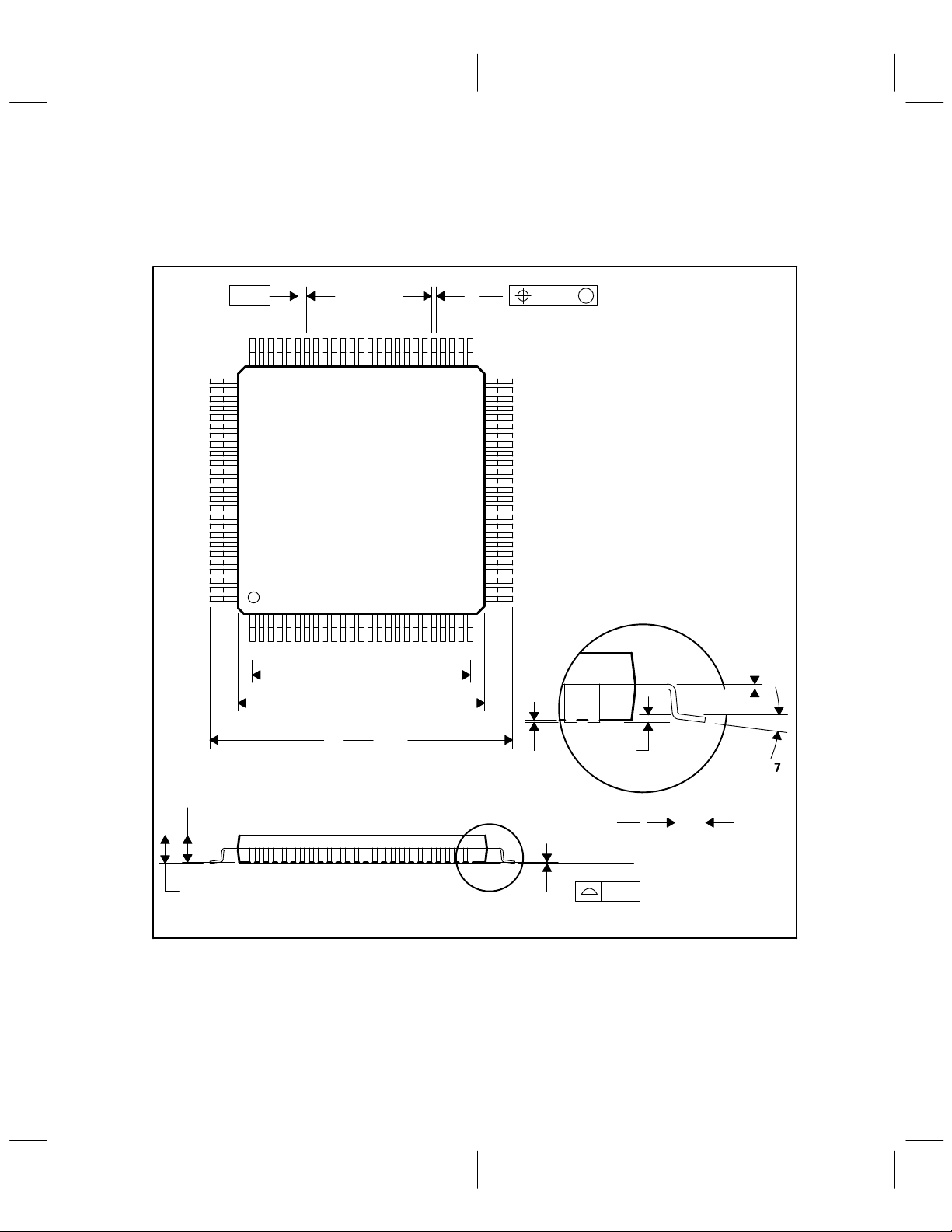
5 Mechanical Data
5.1 PZ (S-PQFP-G100) PLASTIC QUAD FLATPACK
76
100
0,50
75
0,27
0,17
51
50
26
1
12,00 TYP
14,20
SQ
13,80
16,20
SQ
15,80
25
0,05 MIN
0,08
M
0,13 NOM
Gage Plane
0,25
0°–ā7°
1,45
1,35
1,60 MAX
NOTES: A. All linear dimensions are in millimeters.
B. This drawing is subject to change without notice.
C. Falls within JEDEC MO-136
0,75
0,45
Seating Plane
0,08
4040149/A 03/95
5–1
Page 69

IMPORTANT NOTICE
T exas Instruments (TI) reserves the right to make changes to its products or to discontinue any semiconductor
product or service without notice, and advises its customers to obtain the latest version of relevant information
to verify, before placing orders, that the information being relied on is current.
TI warrants performance of its semiconductor products and related software to the specifications applicable at
the time of sale in accordance with TI’s standard warranty. Testing and other quality control techniques are
utilized to the extent TI deems necessary to support this warranty. Specific testing of all parameters of each
device is not necessarily performed, except those mandated by government requirements.
Certain applications using semiconductor products may involve potential risks of death, personal injury, or
severe property or environmental damage (“Critical Applications”).
TI SEMICONDUCTOR PRODUCTS ARE NOT DESIGNED, INTENDED, AUTHORIZED, OR WARRANTED
TO BE SUITABLE FOR USE IN LIFE-SUPPORT APPLICATIONS, DEVICES OR SYSTEMS OR OTHER
CRITICAL APPLICATIONS.
Inclusion of TI products in such applications is understood to be fully at the risk of the customer. Use of TI
products in such applications requires the written approval of an appropriate TI officer . Questions concerning
potential risk applications should be directed to TI through a local SC sales office.
In order to minimize risks associated with the customer’s applications, adequate design and operating
safeguards should be provided by the customer to minimize inherent or procedural hazards.
TI assumes no liability for applications assistance, customer product design, software performance, or
infringement of patents or services described herein. Nor does TI warrant or represent that any license, either
express or implied, is granted under any patent right, copyright, mask work right, or other intellectual property
right of TI covering or relating to any combination, machine, or process in which such semiconductor products
or services might be or are used.
Copyright 1996, Texas Instruments Incorporated
 Loading...