

TCM38C17IDL
QCombo FOUR-CHANNEL (QUAD) PCM COMBO
SLWS040C – JUNE 1996 – REVISED OCTOBER 1999
D
Single 5-V Supply
D
Replaces Four TCM29C13-Type Combos
(CODEC and Filters)
D
Meets CCITT/(D3/D4) G.711 and G.714
Channel Bank Specifications
D
Advanced Switched-Capacitor Filters and
Sigma-Delta A/D and D/A Converter
Technology With DSP Filtering
D
µ-Law or A-Law Companding —
Pin-Selectable
D
2.048 MHz Operation
D
8 Vpp Full-Signal Differential Receiver
Output
D
Differential Signal Processing Architecture
D
Low Crosstalk (< –100 dB),
Low Idle-Channel Noise, and
Good Power Supply Rejection
D
Single PCM I/O for Simplified PCM Interface
D
Reliable Submicron Silicon-Gate CMOS
Technology
description
The TCM38C17IDL QCombo is a 4-channel
single-chip PCM combo (pulse-code-modulated
RBIAS
AREF
A VSS
0GSX
0ANLGIN–
0ANLGIN+
0PWRO+
0GSR
0PWRO–
1GSX
1ANLGIN–
1ANLGIN+
1PWRO+
1GSR
1PWRO–
0PDN
1PDN
VSS
DVSS
DVDD
DVDDPLL
MCLK
DVSSPLL
ASEL
CODEC with a voice-band filtering) device. It
performs the transmit encoding (A/D conversion)
and receive decoding (D/A conversion), as well as the transmit and receive filtering functions required to meet
CCITT G.71 1 and G.714 specifications in a PCM system. Each channel provides all the functions required to
interface a full-duplex, 4-line voice telephone circuit with a TDM (time-division-multiplexed) system. The
TCM38C17IDL is specifically designed for fixed-data-rate applications and is intended to replace four
TCM29C13-type devices.
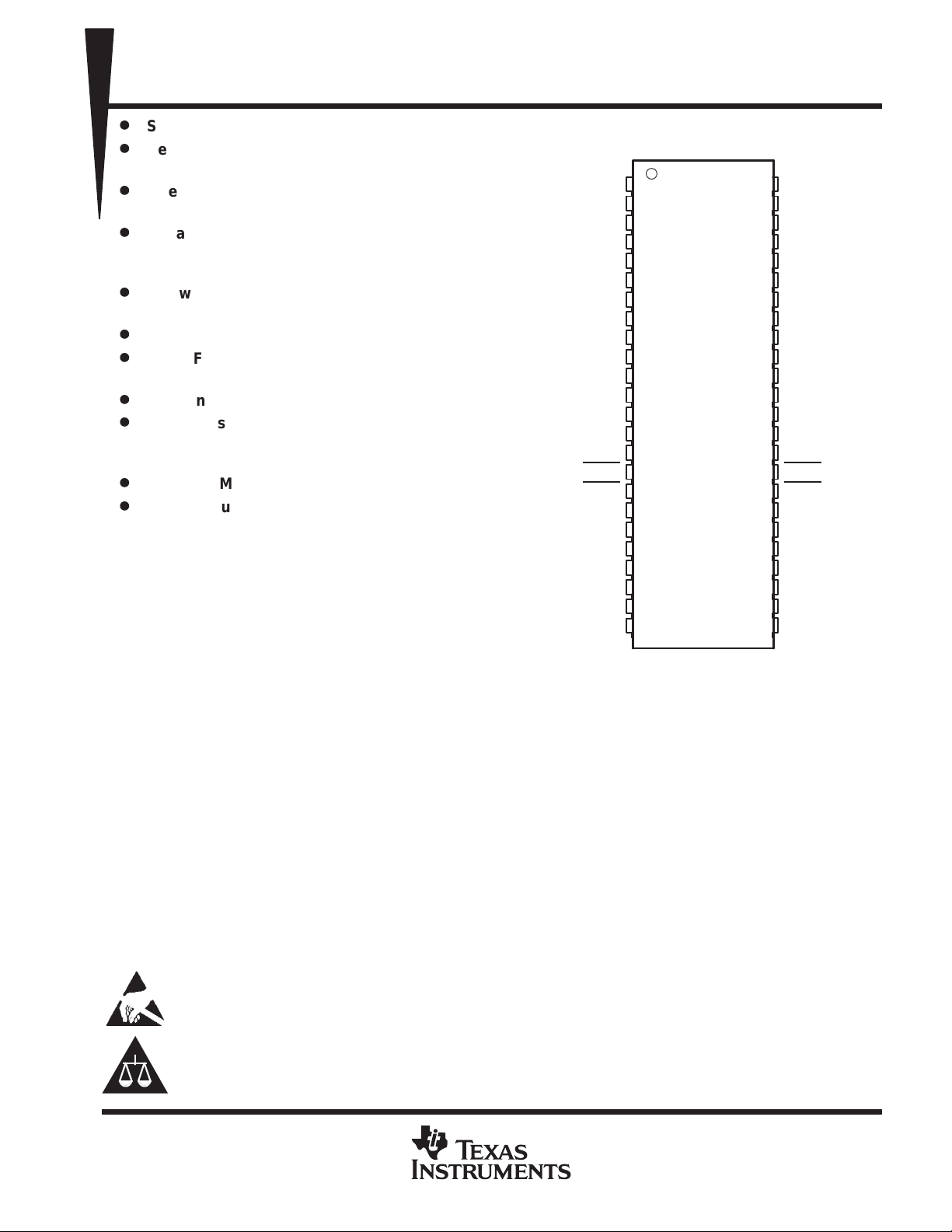
DL PACKAGE
(TOP VIEW)
1
2
3
4
5
6
7
8
9
10
11
12
13
14
15
16
17
18
19
20
21
22
23
24
48
47
46
45
44
43
42
41
40
39
38
37
36
35
34
33
32
31
30
29
28
27
26
25
REFLTR1
REFLTR2
A VDD
2GSX
2ANLGIN–
2ANLGIN+
2PWRO+
2GSR
2PWRO–
3GSX
3ANLGIN–
3ANLGIN+
3PWRO+
3GSR
3PWRO–
3PDN
2PDN
0FS
1FS
2FS
3FS
PCMOUT
RESET
PCMIN
Primary applications include digital transmission and switching of E1 carrier, PABX (private automatic branch
exchange), and central office telephone systems and subscriber line concentrators. The device serves as the
analog termination of a PCM line or trunk to the POTS (plain old telephone system) local-loop line.
Other applications include any PCM digital-audio interface such as voice-band data storage systems and many
digital signal processing applications that can benefit from the reduced footprint of a quad codec configuration
and single-rail operation. Dynamic range and excellent idle-channel noise performance are maintained using
the TI advanced 4Vt process technologies.
These devices have limited built-in ESD protection. The leads should be shorted together or the device placed in conductive foam
during storage or handling to prevent electrostatic damage to the MOS gates.
Please be aware that an important notice concerning availability, standard warranty, and use in critical applications of
Texas Instruments semiconductor products and disclaimers thereto appears at the end of this data sheet.
TI and QCombo are registered trademarks of Texas Instruments, Inc.
PRODUCTION DATA information is current as of publication date.
Products conform to specifications per the terms of Texas Instruments
standard warranty. Production processing does not necessarily include
testing of all parameters.
POST OFFICE BOX 655303 • DALLAS, TEXAS 75265
Copyright 1999, Texas Instruments Incorporated
1
TCM38C17IDL
QCombo FOUR-CHANNEL (QUAD) PCM COMBO
SLWS040C – JUNE 1996 – REVISED OCTOBER 1999
description (continued)
The TCM38C17IDL is available in a 48-pin plastic DL SSOP (shrink small-outline package) and is characterized
for operation from –40°C to 85°C.
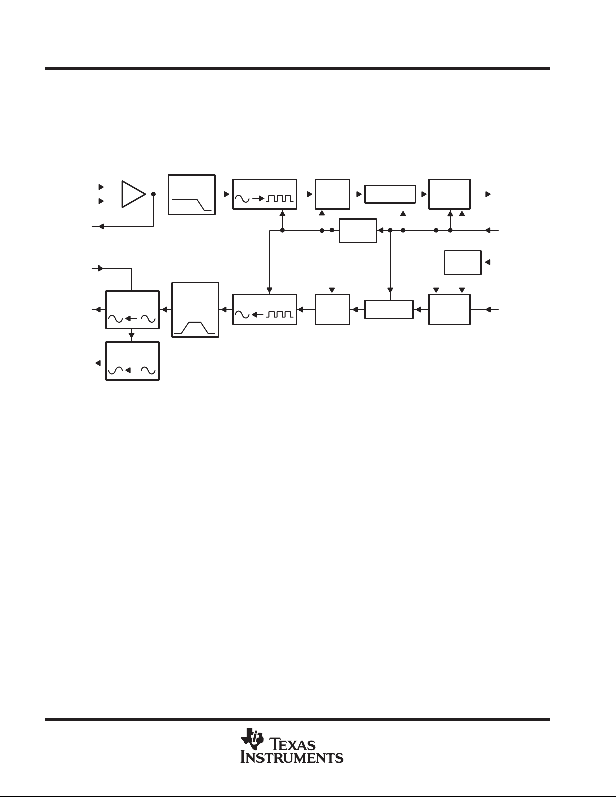
functional block diagram
Analog
Input
ANGLIN–
ANGLIN+
GSX
GSR
PWRO+
Analog
Output
PWRO–
–
+
Output
Amplifier
Inverting
Amplifier
Antialias
Filter
SwitchedCapacitor
Smoothing
Filter
NOTE A: One of four identical channels is depicted.
Σ∆ ADC
Σ∆ DAC
Transmit Section
Digital
Filter
Clock
Buffer
Digital
Filter
Receive Section
Compressor
Expander
Output
Register
Frame
Control
Input
Register
Digital
Output
PCMOUT
MCLK
(2.048 MHz)
FS
PCMIN
Digital
Input
2
POST OFFICE BOX 655303 • DALLAS, TEXAS 75265
I/O
DESCRIPTION
TCM38C17IDL
QCombo FOUR-CHANNEL (QUAD) PCM COMBO
SLWS040C – JUNE 1996 – REVISED OCTOBER 1999
Terminal Functions
TERMINAL
NAME NO.
AREF 2 Analog reference point (mid-supply). This voltage is generated internally at a nominal 2.375 V. An
0ANLGIN+ 6 I Noninverting analog input to uncommitted transmit operational amplifier for channel 0
0ANLGIN– 5 I Inverting analog input to uncommitted transmit operational amplifier for channel 0
1ANLGIN+ 12 I Noninverting analog input to uncommitted transmit operational amplifier for channel 1
1ANLGIN– 11 I Inverting analog input to uncommitted transmit operational amplifier for channel 1
2ANLGIN+ 43 I Noninverting analog input to uncommitted transmit operational amplifier for channel 2
2ANLGIN– 44 I Inverting analog input to uncommitted transmit operational amplifier for channel 2
3ANLGIN+ 37 I Noninverting analog input to uncommitted transmit operational amplifier for channel 3
3ANLGIN– 38 I Inverting analog input to uncommitted transmit operational amplifier for channel 3
ASEL 24 I A-law and µ-law operation select. When ASEL is connected to ground, A-law is selected. When ASEL is
AVDD 46 Analog supply voltage, 5 V , ±5%
AVSS 3 Analog ground return for AVDD supply
DVDD 20 Digital supply voltage, 5 V, ±5%
DVDDPLL 21 Phase-locked loop supply voltage, 5 V, ±5%
DVSSPLL 23 Phase-locked loop ground return for DVDDPLL supply
DVSS 19 Digital ground return for DVDD supply
0FS 31 I Frame synchronization clock input/time slot enable for channel 0 TX and RX (digital)
1FS 30 I Frame synchronization clock input/time slot enable for channel 1 TX and RX (digital)
2FS 29 I Frame synchronization clock input/time slot enable for channel 2 TX and RX (digital)
3FS 28 I Frame synchronization clock input/time slot enable for channel 3 TX and RX (digital)
0GSR 8 I Receive amplifier gain-set input (channel 0). The ratio of an external voltage divider network connected to
1GSR 14 I Receive amplifier gain-set input (channel 1). The ratio of an external voltage divider network connected to
2GSR 41 I Receive amplifier gain-set input (channel 2). The ratio of an external voltage divider network connected to
3GSR 35 I Receive amplifier gain-set input (channel 3). The ratio of an external voltage divider network connected to
0GSX 4 O Output terminal of internal uncommitted transmit operational amplifier for channel 0 (analog)
1GSX 10 O Output terminal of internal uncommitted transmit operational amplifier for channel 1 (analog)
2GSX 45 O Output terminal of internal uncommitted transmit operational amplifier for channel 2 (analog)
3GSX 39 O Output terminal of internal uncommitted transmit operational amplifier for channel 3 (analog)
MCLK 22 I Master clock input (2.048 MHz) (digital)
PCMIN 25 I Transmit PCM input (digital)
PCMOUT 27 O Transmit PCM output (digital)
0PDN 16 I Power-down select for channel 0. This channel of the device is inactive with a CMOS low-level input to
1PDN 17 I Power-down select for channel 1. This channel of the device is inactive with a CMOS low-level input to
2PDN 32 I Power-down select for channel 2. This channel of the device is inactive with a CMOS low-level input to
external decoupling capacitor (0.1 µF) should be connected from AREF to AVSS for filtering purposes.
connected to VDD, µ-law is selected (digital).
0PWRO– and 0PWRO+ determines the receive amplifier gain. Maximum gain occurs when 0GSR is
connected to 0PWRO–, and minimum gain occurs when it is connected to 0PWRO+ (analog).
1PWRO– and 1PWRO+ determines the receive amplifier gain. Maximum gain occurs when 1GSR is
connected to 1PWRO–, and minimum gain occurs when it is connected to 1PWRO+ (analog).
2PWRO– and 2PWRO+ determines the receive amplifier gain. Maximum gain occurs when 2GSR is
connected to 2PWRO–, and minimum gain occurs when it is connected to 2PWRO+ (analog).
3PWRO– and 3PWRO+ determines the receive amplifier gain. Maximum gain occurs when 3GSR is
connected to 3PWRO–, and minimum gain occurs when it is connected to 3PWRO+ (analog).
0PDN
and active with a CMOS high-level input to the terminal (digital).
1PDN
and active with a CMOS high-level input to the terminal (digital).
2PDN
and active with a CMOS high-level input to the terminal (digital).
POST OFFICE BOX 655303 • DALLAS, TEXAS 75265
3
TCM38C17IDL
I/O
DESCRIPTION
QCombo FOUR-CHANNEL (QUAD) PCM COMBO
SLWS040C – JUNE 1996 – REVISED OCTOBER 1999
Terminal Functions (Continued)
TERMINAL
NAME NO.
3PDN 33 I Power-down select for channel 3. This channel of the device is inactive with a CMOS low-level input to 3PDN
and active with a CMOS high-level input to the terminal (digital).
0PWRO+ 7 O Noninverting output of channel 0 power amplifier. 0PWRO+can drive a 600 Ω || 100 pF load differentially
(analog).
0PWRO – 9 O Inverting output of channel 0 power amplifier . 0PWRO– can drive a 600 Ω || 100 pF load differentially (analog).
1PWRO+ 13 O Noninverting output of channel 1 power amplifier. 1PWRO+ can drive a 600 Ω || 100 pF load differentially
(analog).
1PWRO– 15 O Inverting output of channel 1 power amplifier . 1PWRO– can drive a 600 Ω || 100 pF load differentially (analog).
2PWRO+ 42 O Noninverting output of channel 2 power amplifier. 2PWRO+ can drive a 600 Ω || 100 pF load differentially
(analog).
2PWRO– 40 O Inverting output of channel 2 power amplifier . 2PWRO– can drive a 600 Ω || 100 pF load differentially (analog).
3PWRO+ 36 O Noninverting output of channel 3 power amplifier. 3PWRO+ can drive a 600 Ω || 100 pF load differentially
(analog).
3PWRO– 34 O Inverting output of channel 3 power amplifier , 3PWRO– can drive a 600 Ω || 100 pF load differentially (analog).
RBIAS 1 Bias current setting resistor. A 100 kΩ, ± 5% resistor should be connected between terminals RBIAS and AVSS
to set the bias current of the device.
REFLTR1 48 Voltage reference. A 1-µF external decoupling capacitor should be connected from REFLTR1 to AVSS for
filtering purposes.
REFLTR2 47 Voltage reference. A 1-µF external decoupling capacitor should be connected from REFLTR2 to AVSS for
filtering purposes.
RESET 26 I Reset. Reset for all internal registers is initiated when RESET is brought high (digital).
VSS 18 Substrate bias. VSS should be externally connected to AVSS.
absolute maximum ratings over operating free-air temperature range (unless otherwise noted)
†
Supply voltage range, VDD (see Note 1) –0.3 V to 7 V. . . . . . . . . . . . . . . . . . . . . . . . . . . . . . . . . . . . . . . . . . . . . . .
Input voltage range, V
I
Digital ground voltage range, V
O
–0.3 V to 7 V. . . . . . . . . . . . . . . . . . . . . . . . . . . . . . . . . . . . . . . . . . . . . . . . . . . . . . . . . . . . . .
–0.3 V to 7 V. . . . . . . . . . . . . . . . . . . . . . . . . . . . . . . . . . . . . . . . . . . . . . . . . . . . .
Operating free-air temperature range, TA –40°C to 85°C. . . . . . . . . . . . . . . . . . . . . . . . . . . . . . . . . . . . . . . . . . .
Storage temperature range, T
†
Stresses beyond those listed under “absolute maximum ratings” may cause permanent damage to the device. These are stress ratings only, and
functional operation of the device at these or any other conditions beyond those indicated under “recommended operating conditions” is not
implied. Exposure to absolute-maximum-rated conditions for extended periods may affect device reliability.
NOTE 1: Voltage values are with respect to AVSS.
–65°C to 150°C. . . . . . . . . . . . . . . . . . . . . . . . . . . . . . . . . . . . . . . . . . . . . . . . . .
stg
recommended operating conditions (see Notes 2 and 3)
MIN NOM MAX UNIT
Supply voltage, V
High-level input voltage, V
Low-level input voltage, V
Load resistance between PWRO+ and PWRO– (differential), R
Load capacitance between PWRO+ and PWRO– (differential), C
Operating free-air temperature, T
NOTES: 2. To avoid possible damage to these CMOS devices and resulting reliability problems, the power-up procedure described in the device
DD
IH
IL
L
L
A
power-up sequence paragraphs later in this document should be followed.
3. Voltages at analog inputs, outputs and the AVDD terminal are with respect to the AREF terminal. All other voltages are referenced
to the DVSS terminal unless otherwise noted.
4.75 5 5.25 V
0.8 × V
DD
0.2 × V
600 Ω
–40 85 °C
DD
100 pF
V
V
4
POST OFFICE BOX 655303 • DALLAS, TEXAS 75265
IDDSupply current from V
TCM38C17IDL
QCombo FOUR-CHANNEL (QUAD) PCM COMBO
SLWS040C – JUNE 1996 – REVISED OCTOBER 1999
electrical characteristics over recommended ranges of supply voltage and operating free-air
temperature (unless otherwise noted)
supply current, total device, MCLK = 2.048 MHz, outputs not loaded, VDD = 5 V, TA = 25°C
PARAMETER TEST CONDITIONS MIN TYP MAX UNIT
pp
†
With 8 Vpp output
DD
Operating All channels 50
Power down PDN (all channels) 11 mA
digital interface
PARAMETER TEST CONDITIONS MIN TYP MAX UNIT
V
High-level output voltage PCMOUT IOH = –3.2 mA 4.6 5 V
OH
V
Low-level output voltage PCMOUT IOL = 3.2 mA 0 0.4 V
OL
I
High-level input current, any digital input VI = 0.8 × V
IH
I
Low-level input current, any digital input VI = 0.2 × V
IL
C
Input capacitance 5 pF
i
C
Output capacitance 5 pF
o
DD
DD
transmit amplifier input
PARAMETER MIN TYP MAX UNIT
Input current at ANLGIN+ and ANLGIN– ±100 nA
Input offset voltage at ANLGIN+ and ANLGIN– ±5 mV
Common-mode rejection at ANLGIN+ and ANLGIN– 55 dB
Open-loop voltage amplification at ANLGIN+ and ANLGIN– 60 dB
Open-loop unity-gain bandwidth at ANLGIN+ and ANLGIN– 900 kHz
Input resistance at ANLGIN+ and ANLGIN– 10 MΩ
†
mA
10 µA
10 µA
receive filter output
PARAMETER TEST CONDITION MIN TYP‡MAX UNIT
Output offset voltage at PWRO+/PWRO – Relative to AREF ±80 mV
Output resistance at PWRO+/PWRO – DC output 1 Ω
‡
All typical values are at VDD = 5 V, and TA = 25_C.
POST OFFICE BOX 655303 • DALLAS, TEXAS 75265
5
TCM38C17IDL
(),
Vrms
(),
R
L
600 Ω at maximum gain
Vrms
QCombo FOUR-CHANNEL (QUAD) PCM COMBO
SLWS040C – JUNE 1996 – REVISED OCTOBER 1999
electrical characteristics over recommended ranges of supply voltage and operating free-air
temperature (unless otherwise noted) (continued)
transmit and receive gain and dynamic range, V
PARAMETER TEST CONDITION MIN TYP MAX UNIT
Encoder milliwatt response (transmit gain tolerance) Signal input = 0 dBm0 ±0.1 ±0.18 dBm0
Encoder milliwatt response variation with temperature and
power supplies
Digital milliwatt response (receive tolerance gain) relative to
zero-transmission-level point
Digital milliwatt response variation with temperature and power
supplies
Zero-transmission–level point (0 dBm0), transmit
channel
Transmit overload signal level, peak-to-peak centered at AREF 3 Vpp
Zero-transmission–level point (0 dBm0), receive
channel
Receive overload signal level, fully differential
NOTES: 4. Unless otherwise noted, the analog input is a 0-dBm0, 1020-Hz sine wave, where 0 dBm0 is defined as the zero-reference point of
the channel under test.
5. The input amplifier is set for noninverting unity gain. The digital input is a PCM bit stream generated by passing a 0-dBm0, 1020-Hz
sine wave through an ideal encoder.
6. Receive output is measured single ended in the maximum-gain (unity) configuration. To set the output amplifier for maximum gain,
GSR is connected to PWRO– and the output is taken at PWRO+. All output levels are (sin x)/x corrected.
µ-law 0.747
A-law
µ-law
A-law
= 5 V, TA = 25°C (see Notes 4, 5, and 6)
DD
TA = –40°C to 85°C, Supplies = ±5% ±0.08 dB
Signal input per CCITT G.711 ±0.1 ±0.18 dBm0
TA = –40°C to 85°C,
Supplies = ±5%
Input buffer configured for unity gain
=
=
(Load is connected between
PWRO+ and PWRO–)
7.8 8 Vpp
±0.08 dB
0.75
1.99
2
transmit and receive gain tracking over recommended ranges of supply voltage and operating free-air
temperature, reference level = –10 dBm0
PARAMETER TEST CONDITION MIN TYP MAX UNIT
3 > input level ≥ – 40 dBm0 ±0.25
Transmit gain tracking error , sinusoidal input
Receive gain tracking error, sinusoidal input
–40 > input level > –50 dBm0 ±0.5
–50 ≥ input level ≥ – 55 dBm0 ±1.2
3 > input level ≥ – 40 dBm0 ±0.25
–40 > input level > –50dBm0 ±0.5
–50 ≥ input level ≥ – 55 dBm0 ±1.2
dB
dB
noise over recommended ranges of supply voltage and operating free-air temperature
Transmit noise, C-message weighted (µ-law), PCMOUT ANLGIN+ = 0 V 10 12 dBrnC0
Transmit noise, psophometrically weighted (A-law), PCMOUT ANLGIN+ = 0 V –80 –75 dBm0p
Receive noise, C-message-weighted quiet code at PWRO+ (µ-law) PCMIN = 11111111 5 12 dBrnC0
Receive noise, psophometrically weighted at PWRO+ (A-law) PCMIN = 11010101 –85 –79 dBm0p
6
PARAMETER TEST CONDITION MIN TYP MAX UNIT
POST OFFICE BOX 655303 • DALLAS, TEXAS 75265
V
suppl
oltage rejection, transmit channel
Supply signal
200 mVpp
dB
y
DD
ygj ,
Su ly signal 200 mV ,
dB
Crosstalk (between channels) attenuation
0 dBm0
300 H
3400 H
dB
Method 2)
Method 2)
,
dBm0
TCM38C17IDL
QCombo FOUR-CHANNEL (QUAD) PCM COMBO
SLWS040C – JUNE 1996 – REVISED OCTOBER 1999
electrical characteristics over recommended ranges of supply voltage and operating free-air
temperature (unless otherwise noted) (continued)
power supply rejection and crosstalk attenuation over recommended ranges of supply voltage and
operating free-air temperature
PARAMETER TEST CONDITION MIN TYP†MAX UNIT
pp
y v
DD
V
supply voltage rejection, receive channel
(single-ended)
Crosstalk (same channel) attenuation, transmit-to-receive
(single-ended)
Crosstalk (same channel) attenuation, receive-to-transmit
(single-ended)
†
All typical values are at VDD = 5 V, and TA = 25°C
‡
Actual levels were beneath the test equipment measurement floor.
0 < f < 30 kHz
30 < f < 50 kHz
0 < f < 30 kHz
30 < f< 50 kHz
Transmit to transmit ≤100
Transmit to receive
Receive to transmit
Receive to receive ≤100
Idle channel,
pp
f measured at PCMOUT
Idle channel,
Suppl
narrow-band,
f measured at PWRO+
ANLGIN+ = 0 dBm0,
f = 1.02 kHz, unity gain,
PCMIN = lowest decode level,
measured at PWRO+
PCMIN = 0 dBm0,
f = 1.02 kHz,
measured at PCMOUT
=
signal = 200 mVpp,
,
z –
pp
,
–40
–45
–40
–45
‡
≤100
≤100
z
≤100
≤100
‡
‡
‡
‡
‡
–75 dB
–75 dB
–76
–78
–76
–78
distortion over recommended ranges of supply voltage and operating free-air temperature
PARAMETER TEST CONDITIONS MIN MAX UNIT
Transmit signal to distortion ratio, sinusoidal input (CCITT G.712 -
Receive signal to distortion ratio, sinusoidal input (CCITT G.712 -
Transmit single-frequency distortion products Input signal = 0 dBm0 –46 dBm0
Receive single-frequency distortion products Input signal = 0 dBm0 –46 dBm0
Intermodulation distortion, end-to-end
Spurious out-of-band signals, end-to-end
0 > ANLGIN > –30 dBm0 36
–30 > ANLGIN > –40 dBm0 30
–40 > ANLGIN > –45 dBm0 25
0 > ANLGIN > –30 dBm0 36
–30 > ANLGIN > –40 dBm0 30
–40 > ANLGIN > –45 dBm0 25
CCITT G.712 (7.1) –35
CCITT G.712 (7.2) –49
CCITT G.712 (6.1) –25
CCITT G.712 (9) –40
dB
dB
POST OFFICE BOX 655303 • DALLAS, TEXAS 75265
7

TCM38C17IDL
1.02 kHz
Noninverting maximum gain output
g
dB
g
(g ) g
g
dB
QCombo FOUR-CHANNEL (QUAD) PCM COMBO
SLWS040C – JUNE 1996 – REVISED OCTOBER 1999
electrical characteristics over recommended ranges of supply voltage and operating free-air
temperature (unless otherwise noted) (continued)
transmit filter transfer over recommended ranges of supply voltage and operating free-air temperature
(see Figure 1)
PARAMETER TEST CONDITION MIN MAX UNIT
16.67 Hz –30
50 Hz –25
60 Hz –23
Gain (voltage amplification) relative to gain at
receive filter transfer over recommended ranges of supply voltage and operating free-air temperature
(see Figure 2)
PARAMETER TEST CONDITION MIN MAX UNIT
Gain (voltage amplification) relative to gain at 1.02 kHz Input signal at PCMIN
Input amplifier set for unity gain,
Input si
nal at ANLGIN is 0 dBm0
is 0 dBm0
p
300 Hz to 3 kHz –0.15 0.15
3.3 kHz –0.35 0.15
3.4 kHz –1 –0.1
4 kHz –14
Below 20 Hz 0.15
20 Hz 0.15
200 Hz –0.5 0.15
300 Hz to 3 kHz –0.15 0.15
3.3 kHz –0.35 0.15
3.4 kHz –1 –0.1
4 kHz –14
4.6 kHz and above –30
200 Hz –1.8 –0.125
,
timing requirements
clock timing requirements over recommended ranges of supply voltage and operating free-air temperature
(see Figures 3 and 4)
MIN NOM†MAX UNIT
t
c(MCLK)
t
r
t
f
t
w(MCLK)
†
All nominal values are at VDD = 5 V, and TA = 25°C.
NOTE 7: FS clock must be phase-locked with MCLK.
Clock period for MCLK 2.048 MHz systems 488.28 ns
Rise time for MCLK 30 ns
Fall time for MCLK 30 ns
Pulse duration for MCLK (see Note 8) 220 ns
Clock duty cycle [t
w(MCLK)/tc(MCLK)
] for MCLK 45% 50% 55%
8
POST OFFICE BOX 655303 • DALLAS, TEXAS 75265

y
s
y
s
TCM38C17IDL
QCombo FOUR-CHANNEL (QUAD) PCM COMBO
SLWS040C – JUNE 1996 – REVISED OCTOBER 1999
timing requirements over recommended ranges of supply voltage and operating free-air temperature,
fixed-data-rate mode (see Figures 3 and 4)
MIN MAX UNIT
t
su(FS)
t
su(PCMIN)
t
h(PCMIN)
t
h(RESET)
t
h(FS)
t
d(FS–FS)
switching characteristics
propagation delay times over recommended ranges of operating conditions, fixed-data-rate mode (see
Figure 3)
t
pd1
t
pd2
t
pd3
NOTE 8: Timing parameters t
absolute and relative delay times over recommended ranges of supply voltage and operating free-air
temperature
Transmit absolute delay time to PCMOUT
Transmit differential envelope delay time
relative to transmit absolute delay time
Receive absolute delay time to PWRO
Receive differential envelope delay time
relative to transmit absolute delay time
†
All typical values are at VDD = 5 V, and TA = 25°C.
Setup time, frame sync, from FS↑ to MCLK↓ 100 tc (MCLK) –100 ns
Setup time, receive data, from data valid to MCLK↓ 10 ns
Hold time, receive data, from MCLK↓ to data invalid 60 ns
Hold time, RESET terminal ↑ to reset activation 100 ns
Hold time, frame sync, from MCLK↑ to FS↓ 10
Delay time, between MCLK↓ while any channel FS high and MCLK↓ while next
channel FS high (see Figure 6)
PARAMETER TEST CONDITION MIN MAX UNIT
Transmit clock↑ to bit 1 data valid at PCMOUT (data enable time on time slot
entry) (see Note 8)
Transmit clock↑ bit n to bit n data valid at PCMOUT (data valid time) CL = 0 to 100 pF 0 145 ns
Transmit clock↓ bit 8 to bit 8 hi-Z at PCMOUT (data float time on time slot exit)
(see Note 9)
and t
pd1
PARAMETER TEST CONDITION MIN TYP†MAX UNIT
are referenced to the high-impedance state.
pd3
Fixed data rate,
MCLK = 2.048 MHz,
Input to ANLGIN 1.02 kHz at 0 dBm0
f = 500 Hz – 600 Hz 170
f = 600 Hz – 1000 Hz 95
f = 1000 Hz – 2600 Hz 45
f = 2600 Hz – 2800 Hz 105
Fixed data rate,
MCLK = 2.048 MHz,
Digital input is digital milliwatt codes
f = 500 Hz – 600 Hz 45
f = 600 Hz – 1000 Hz 35
f = 1000 Hz – 2600 Hz 85
f = 2600 Hz – 2800 Hz 110
CL = 0 to 100 pF 0 145 ns
CL = 0 pF 60 215 ns
tc(MCLK)×7
tc(MCLK)×64
500 µs
190 µs
ns
µs
µ
µ
POST OFFICE BOX 655303 • DALLAS, TEXAS 75265
9

TCM38C17IDL
QCombo FOUR-CHANNEL (QUAD) PCM COMBO
SLWS040C – JUNE 1996 – REVISED OCTOBER 1999
PARAMETER MEASUREMENT INFORMATION
0
–1
0
–10
–20
Gain Relative to Gain at 1 kHz – dB
V
–30
A –
–30 dB
16.67 Hz
–23 dB
60 Hz
–25 dB
50 Hz
–0.125 dB
200 Hz
–1.8 dB
200 Hz
0.15 dB
300 Hz
–0.15 dB
300 Hz
Typical Filter
Transfer Function
Typical Filter
Transfer Function
0.15 dB
3000 Hz
–0.15 dB
3000 Hz
–0.35 dB
3300 Hz
–1dB
3400 Hz
0.15 dB
3300 Hz
–0.1 dB
3400 Hz
–14 dB
4000 Hz
–32 dB
4600 Hz
0
Expanded Scale
–1
0
–10
–20
–30
–40
–60 –60
10 k1 k1005010
f – Frequency – Hz
NOTE A: Gain (voltage amplification) is defined as gain relative to gain at 1 kHz –dB.
Figure 1. Transmit-Filter Transfer Characteristics
–40
–50–50
10
POST OFFICE BOX 655303 • DALLAS, TEXAS 75265

TCM38C17IDL
QCombo FOUR-CHANNEL (QUAD) PCM COMBO
SLWS040C – JUNE 1996 – REVISED OCTOBER 1999
PARAMETER MEASUREMENT INFORMATION
+2
+1
0.15 dB
200 Hz
0
–0.5 dB
200 Hz
–1
0
–10
– Gain Relative to Gain at 1 kHz – dB
V
–20
A
0.15 dB
300 Hz
–0.15 dB
300 Hz
–0.15 dB
3000 Hz
–0.35 dB
3300 Hz
0.15 dB
3000 HZ
–1dB
3400 Hz
0.15 dB
3300 HZ
–0.10 dB
3400 Hz
–14 dB
4000 Hz
+2
+1
0
–1
0
–10
–20
Expanded Scale
–30
–40
–50
–60
1 k100
f – Frequency – Hz
NOTE A: Gain (voltage amplification) is defined as gain relative to gain at 1 kHz –dB.
Transfer Function
Figure 2. Receive-Filter Transfer Characteristics
Typical Filter
–30 dB
4800 Hz
–30
–40
–50
–60
10 k
POST OFFICE BOX 655303 • DALLAS, TEXAS 75265
11

TCM38C17IDL
QCombo FOUR-CHANNEL (QUAD) PCM COMBO
SLWS040C – JUNE 1996 – REVISED OCTOBER 1999
PARAMETER MEASUREMENT INFORMATION
Time Slot 1
MCLK
t
su(FS)
FS
t
pd1
PCMOUT
†
Bit 1 = MSB = most significant bit and is clocked in first on the PCMIN terminal or is clocked out first on the PCMOUT terminal.
‡
Bit 8 = LSB = least significant bit and is clocked in last on the PCMIN terminal or is clocked out last on the PCMOUT terminal.
12345678
t
h(FS)
Bit 1
t
r
t
pd2
†
Bit 2 Bit 3 Bit 4 Bit 5 Bit 6 Bit 7 Bit 8
t
f
t
w(MCLK)
t
c(MCLK)
t
pd3
Figure 3. PCM Transmit Timing
Time Slot 1
MCLK
t
FS
PCMIN
su(FS)
t
su(PCMIN)
12345678
Bit 1
Valid
t
†
h(FS)
t
r
t
h(PCMIN)
Bit 2
Valid
Bit 3
Valid
t
f
Bit 4
Valid
t
w(MCLK)
Bit 5
Valid
Bit 6
Valid
t
c(MCLK)
Bit 7
Valid
Bit 8
Valid
‡
‡
†
Bit 1 = MSB = most significant bit and is clocked in first on the PCMIN terminal or is clocked out first on the PCMOUT terminal.
‡
Bit 8 = LSB = least significant bit and is clocked in last on the PCMIN terminal or is clocked out last on the PCMOUT terminal.
Figure 4. PCM Receive Timing
12
POST OFFICE BOX 655303 • DALLAS, TEXAS 75265

TCM38C17IDL
QCombo FOUR-CHANNEL (QUAD) PCM COMBO
SLWS040C – JUNE 1996 – REVISED OCTOBER 1999
PRINCIPLES OF OPERATION
system reliability and design considerations
The TCM38C17IDL system reliability and design considerations are described in the following paragraphs.
latch-up
Latch-up is possible in all CMOS devices. It is caused by the firing of a parasitic SCR that is present due to the
inherent nature of CMOS. When a latch-up occurs, the device draws excessive amounts of current and will
continue to draw heavy current until power is removed. Latch-up can result in permanent damage to the device
if supply current to the device is not limited.
Even though the QCombo is heavily protected against latch-up, it is still possible to cause latch-up under certain
conditions in which excess current is forced into or out of one or more terminals. Latch-up can occur when the
supply voltage drops momentarily below ground or possibly if a signal is applied to a terminal after power has
been applied but before the ground is connected. This can happen if the device is hot inserted into a card with
the power applied, or if the device is mounted on a card that has an edge connector and the card is hot inserted
into a system with the power on.
To help ensure that latch-up does not occur, it is considered good design practice to connect a reverse-biased
Schottky diode with a forward voltage drop of less than or equal to 0.4 V (1N5711 or equivalent) between the
power supply and GND (see Figure 5). It is possible that a QCombo-equipped card with an edge connector can
not be hot inserted into a powered-up system. In this case, it is also important to ensure that the ground edge
connector traces are longer than the power and signal traces so that the card ground is always the first to make
contact.
V
DD
GND
Figure 5. Latch-Up Protection Diode Connection
device power-up sequence
Latch-up also can occur if a signal source is connected without the device being properly grounded. A signal
applied to one terminal could then find a ground through another signal terminal on the device. T o ensure proper
operation of the device and as a safeguard against this sort of latch-up, it is recommended that the following
power-up sequence always be used:
1. Ensure that no signals are applied to the device before the power-up sequence is complete.
2. Connect GND.
3. Apply power.
4. Force a power down-condition in the device.
5. Connect the master clock.
6. Release the power-down condition.
7. Apply FS synchronization pulses.
8. Apply the analog signal inputs.
When powering down the device, this procedure should be followed in the reverse order.
POST OFFICE BOX 655303 • DALLAS, TEXAS 75265
13

TCM38C17IDL
QCombo FOUR-CHANNEL (QUAD) PCM COMBO
SLWS040C – JUNE 1996 – REVISED OCTOBER 1999
PRINCIPLES OF OPERATION
system reliability and design considerations (continued)
internal sequencing
On the transmit channel, digital output PCMOUT is held in the high-impedance state for approximately four
frames (500 µs) after power up. Frame sync must be applied to all four channels during this time. After this delay ,
PCMOUT is functional and occurs in the proper timeslot. Valid digital information, such as for on/off hook
detection, is available almost immediately.
To further enhance system reliability, PCMOUT is placed in a high-impedance state approximately 20 µs after
an interruption of MCLK. This interruption could possibly occur with some kind of fault condition elsewhere in
the system.
power-down operation
T o minimize power consumption, a power-down mode is provided for each channel. To power down a channel,
an external logic low signal is applied to the corresponding PDN terminal. In the power-down mode, the average
power consumption is reduced to an average of 1 mW/channel.
miscellaneous
TCM38C17IDL timing and voltage references are described in the following paragraphs.
data timing
The TCM38C17IDL uses the 2.048 MHz master clock input to step data into and out of the device. An 8-kHz
clock signal applied to the FS terminal sets the sampling frequency and indicates the beginning of data transfer.
When MCLK goes low while FS is high, the frame sync is recognized. The next eight rising edges of MCLK step
data out of PCMOUT, while data is received into PCMIN on the next eight falling edges of MCLK. It is
recommended that frame sync pulses be one MCLK period in duration, but it is permissible for them to last up
to seven MCLK periods from the recognition of the frame sync.
Frame syncs for channels 0 through 3 must occur sequentially. When all four channels are in use, the frame
syncs (downward edge of MCLK during frame sync high) must occur at nominal 64 MCLK pulse intervals,
making the frame syncs evenly distributed. When one or more channels are not in use, the active frame syncs
have greater timing flexibility , but still must be separated by a minimum of 64 MCLK periods (nominal 31.25 µs
with 2.048 MHz MCLK). See Figure 6.
14
POST OFFICE BOX 655303 • DALLAS, TEXAS 75265

QCombo FOUR-CHANNEL (QUAD) PCM COMBO
PRINCIPLES OF OPERATION
system reliability and design considerations (continued)
125 µs
MCLK
0FS
31.25 µs
1FS
31.25 µs
2FS
3FS
TCM38C17IDL
SLWS040C – JUNE 1996 – REVISED OCTOBER 1999
31.25 µs
PCM
In/Out
MCLK
0FS
1FS
2FS
3FS
Data
In/Out
Channel 0
Data In/Out
8 Clocks
Channel 1
Data In/Out
Channel 2
Data In/Out
64 Clocks
31.25 µs @
2.048 MHz
MCLK
31.25 µs
Channel 3
Data In/Out
Figure 6. Frame Sync Timing
POST OFFICE BOX 655303 • DALLAS, TEXAS 75265
15

TCM38C17IDL
QCombo FOUR-CHANNEL (QUAD) PCM COMBO
SLWS040C – JUNE 1996 – REVISED OCTOBER 1999
PRINCIPLES OF OPERATION
system reliability and design considerations (continued)
precision voltage references
It is recommended that an external 1-µF capacitor be connected between REFLTR1 and A VSS and between
REFLTR2 and AVSS to ensure clean voltage references. Voltage references that determine the gain and
dynamic range characteristics of the device are generated internally . A band-gap mechanism is used to derive
a temperature-independent and bias-stable reference voltage. These references are calibrated during the
manufacturing process. Separate references are supplied to the transmit and receive sections, and each is
calibrated independently . Each reference value is then further trimmed in the gain-setting operational amplifiers
to a final precision value. Manufacturing tolerances of typically ±0.1 dB in absolute gain (voltage amplification)
can be achieved for each half channel, providing the user a significant margin to compensate for error in other
board components.
transmit operation
The TCM38C17IDL transmit operation is described in the following paragraphs.
transmit input amplifier
The input section provides gain adjustment in the passband by means of an on-chip uncommitted operational
amplifier. Gain for the amplifier is set using external input and feedback resistors as shown in Figure 7. This
allows maximum flexibility in presetting volume levels. Unity gain can be achieved by assigning RI and RF equal
values. The feedback impedance between GSX and ANLGIN should be greater than 10 kΩ in parallel with less
than 50 pF. GSX also provides a means of sampling the amplified signal.
GSX
R
F
R
I
AREF
External
ANLGIN–
ANLGIN+
–
+
Internal
A = –
ADC
R
F
R
I
Figure 7. Transmit Path Gain Setting Circuitry
transmit filter
The transmit filters provide passband flatness and stopband attenuation that fulfills the AT&T D3/D4 channel
bank transmission specification and CCITT recommendation G.712. The device specifications meet or exceed
digital class 5 central office switching systems requirements.
A high-pass section configuration was chosen to reject low-frequency noise from 50- and 60-Hz power lines,
17-Hz European electric railroads, ringing frequencies and their harmonics, and other low-frequency noise.
Even with the high rejection at these frequencies, the sharpness of the band edge gives low attenuation at
200 Hz. This feature allows the use of low-cost transformer hybrids without external components.
16
POST OFFICE BOX 655303 • DALLAS, TEXAS 75265

TCM38C17IDL
QCombo FOUR-CHANNEL (QUAD) PCM COMBO
SLWS040C – JUNE 1996 – REVISED OCTOBER 1999
PRINCIPLES OF OPERATION
receive operation
The TCM38C17IDL receive operation is described in the following paragraphs.
receive filter
The receive filters provide pass-band flatness and stopband rejection that fulfills both the AT&T D3/D4
specification and CCITT recommendation G.712. The filter contains the required compensation for the (sin x)/x
response of such decoders.
output amplifier
The QCombo incorporates a versatile analog output power amplifier than can drive transformer hybrids or
low-impedance loads directly in either a single-ended or differential configuration. The QCombo output stage
allows for volume control (in the differential mode) by connection of a resistor divider chain to the output
terminals of the device. The inverting operational amplifier can drive a 600 Ω load in parallel with 100 pF . Figure 8
is a representation of the internal structure of the output amplifier.
R
F
DAC
R1
R2
_
+
R
INV
PWRO+
+
_
GSR
PWRO–
Internal
External
_
+
AREF
Unity Gain
Inverter
R
INV
AREF
Figure 8. Output Amplifier Architecture
R
GSR1
R
GSR2
POST OFFICE BOX 655303 • DALLAS, TEXAS 75265
17

TCM38C17IDL
QCombo FOUR-CHANNEL (QUAD) PCM COMBO
SLWS040C – JUNE 1996 – REVISED OCTOBER 1999
APPLICATION INFORMATION
Various TCM38C17IDL output configurations are detailed in the following paragraphs.
differential configuration
For connection to a transformer, the fully differential configuration is recommended to provide maximum
possible output, or voltage swing, to the primary of an attached transformer. Figure 9 shows the QCombo in a
fully-differential mode.
PWRO+
R1
GSR
R2
PWRO–
V
O+
R
L
V
O–
Vd
Figure 9. Fully Differential Gain-Setting Configuration
PWRO+ and PWRO– are low-impedance complementary outputs. The total output available for the output load
(R
) is then VD = VO+ – VO–. R1 and R2 form a gain-setting resistor network with a center tap connected to the
L
GSR input.
R1 + R2 should be greater than 10 kΩ and less than 100 kΩ because the parallel combination R1 + R2 and R
sets the total loading. The total parasitic capacitance of the GSR input, along with the parallel combination of
R1 and R2, define a time constant that must be minimized to avoid inaccuracies in the gain calculations.
The resistor gain control actually consists of attenuating the full differential output voltage. The equation to
determine the value of the attenuation constant is given in equation 1.
A
+
1
)(R1BR2
4
)(R1BR2
)
)
(1)
which can also be expressed as shown in equation 2.
A
R1)R2
+
4(R2)R1B4
)
(2)
L
where A = attenuation constant
Depending on the values of gain setting resistors R1 and R2, the attenuation constant (A) can have a value of
0.25 to unity (1), or approximately 12 dB of voltage adjustment.
18
POST OFFICE BOX 655303 • DALLAS, TEXAS 75265

TCM38C17IDL
QCombo FOUR-CHANNEL (QUAD) PCM COMBO
SLWS040C – JUNE 1996 – REVISED OCTOBER 1999
APPLICATION INFORMATION
differential configuration (continued)
Maximum output (A = 1) can be obtained by maximizing R1 and minimizing R2. This can be done by letting
R1 = infinity and R2 = 0 Ω (connect GSR to PWRO–), as shown in Figure 10. Referring to the transmit and
receive gain and dynamic range specifications, a maximum output of approximately 8 Vpp can be expected in
this configuration with a load ≥ 600 Ω. See the maximum analog output section for more detail on the digital input
required for maximum analog output.
PWRO+
GSR
PWRO–
V
O+
R
L
V
O–
Figure 10. Fully Differential Maximum Gain-Setting Configuration (A = 1)
Figure 11 illustrates the QCombo with the resistor gain-control setting for an attenuation of A = 0.625.
PWRO+
10 kΩ
GSR
2.5 kΩ
PWRO–
V
O+
R
L
V
O–
Figure 11. Fully Differential Mid-Gain-Setting Configuration (A = 0.625)
Shown in Figure 12, a minimum output (A = 0.25 dB) can be obtained by letting R1 = 0 Ω (connect GSR to
PWRO+), and R2 = infinity.
PWRO+
GSR
PWRO–
V
O+
R
L
V
O–
Figure 12. Fully Differential Minimum-Gain-Setting Configuration (A = 0.25)
POST OFFICE BOX 655303 • DALLAS, TEXAS 75265
19

TCM38C17IDL
QCombo FOUR-CHANNEL (QUAD) PCM COMBO
SLWS040C – JUNE 1996 – REVISED OCTOBER 1999
APPLICATION INFORMATION
single-ended configuration
Figure 13 illustrates the QCombo in a typical single-ended configuration. Gain is set by manipulating the resistor
network in the same way as detailed for the differential mode. A SLIC should be ac-coupled to the TCM38C17.
PWR+
R1
GSR
R2
PWR–
AREF
Figure 13. Single-Ended Configuration
R
L
20
POST OFFICE BOX 655303 • DALLAS, TEXAS 75265

TCM38C17IDL
QCombo FOUR-CHANNEL (QUAD) PCM COMBO
SLWS040C – JUNE 1996 – REVISED OCTOBER 1999
MECHANICAL DATA
DL (R-PDSO-G**) PLASTIC SMALL-OUTLINE PACKAGE
48 PIN SHOWN
0.025 (0,635)
0.012 (0,305)
0.008 (0,203)
48
0.005 (0,13)
25
0.299 (7,59)
0.291 (7,39)
M
0.420 (10,67)
0.395 (10,03)
0.006 (0,15) NOM
Gage Plane
0.010 (0,25)
1
A
0.110 (2,79) MAX
NOTES: A. All linear dimensions are in inches (millimeters).
B. This drawing is subject to change without notice.
C. Body dimensions do not include mold flash or protrusion not to exceed 0.006 (0,15).
D. Falls within JEDEC MO-118
0.008 (0,20) MIN
DIM
A MAX
A MIN
24
PINS **
0.380
(9,65)
0.370
(9,40)
Seating Plane
0.004 (0,10)
4828
0.630
(16,00)
0.620
(15,75)
0°–8°
0.040 (1,02)
0.020 (0,51)
56
0.730
(18,54)
0.720
(18,29)
4040048/C 03/97
POST OFFICE BOX 655303 • DALLAS, TEXAS 75265
21

IMPORTANT NOTICE
T exas Instruments and its subsidiaries (TI) reserve the right to make changes to their products or to discontinue
any product or service without notice, and advise customers to obtain the latest version of relevant information
to verify, before placing orders, that information being relied on is current and complete. All products are sold
subject to the terms and conditions of sale supplied at the time of order acknowledgement, including those
pertaining to warranty, patent infringement, and limitation of liability.
TI warrants performance of its semiconductor products to the specifications applicable at the time of sale in
accordance with TI’s standard warranty. Testing and other quality control techniques are utilized to the extent
TI deems necessary to support this warranty . Specific testing of all parameters of each device is not necessarily
performed, except those mandated by government requirements.
CERTAIN APPLICA TIONS USING SEMICONDUCTOR PRODUCTS MAY INVOL VE POTENTIAL RISKS OF
DEATH, PERSONAL INJURY, OR SEVERE PROPERTY OR ENVIRONMENTAL DAMAGE (“CRITICAL
APPLICATIONS”). TI SEMICONDUCTOR PRODUCTS ARE NOT DESIGNED, AUTHORIZED, OR
WARRANTED TO BE SUITABLE FOR USE IN LIFE-SUPPORT DEVICES OR SYSTEMS OR OTHER
CRITICAL APPLICA TIONS. INCLUSION OF TI PRODUCTS IN SUCH APPLICATIONS IS UNDERST OOD TO
BE FULLY AT THE CUSTOMER’S RISK.
In order to minimize risks associated with the customer’s applications, adequate design and operating
safeguards must be provided by the customer to minimize inherent or procedural hazards.
TI assumes no liability for applications assistance or customer product design. TI does not warrant or represent
that any license, either express or implied, is granted under any patent right, copyright, mask work right, or other
intellectual property right of TI covering or relating to any combination, machine, or process in which such
semiconductor products or services might be or are used. TI’s publication of information regarding any third
party’s products or services does not constitute TI’s approval, warranty or endorsement thereof.
Copyright 1999, Texas Instruments Incorporated
 Loading...