

Texas Instruments SN54AS576J, SN54ALS576BJ, SN74ALS576BDW, SN74ALS576BDWR, SN74ALS576BN Datasheet
...
SN54ALS576B, SN54AS576
SN74ALS576B, SN74ALS577A, SN74AS576
OCTAL D-TYPE EDGE-TRIGGERED FLIP-FLOPS WITH 3-STATE OUTPUTS
SDAS065B – DECEMBER 1982 – REVISED JANUARY 1995
• 3-State Buffer-Type Inverting Outputs Drive
Bus Lines Directly
• Bus-Structured Pinout
• Buffered Control Inputs
• SN74ALS577A Has Synchronous Clear
• Package Options Include Plastic
Small-Outline (DW) Packages, Ceramic
Chip Carriers (FK), Standard Plastic (N, NT)
and Ceramic (J) 300-mil DIPs, and Ceramic
Flat (W) Packages
description
These octal D-type edge-triggered flip-flops
feature 3-state outputs designed specifically for
bus driving. They are particularly suitable for
implementing buffer registers, I/O ports,
bidirectional bus drivers, and working registers.
These flip-flops enter data on the low-to-high
transition of the clock (CLK) input.
The output-enable (OE
internal operations of the flip-flops. Old data can
be retained or new data can be entered while the
outputs are disabled.
The SN54ALS576B and SN54AS576 are
characterized for operation over the full military
temperature range of –55°C to 125°C. The
SN74ALS576B, SN74ALS577A, and
SN74AS576 are characterized for operation from
0°C to 70°C.
) input does not affect
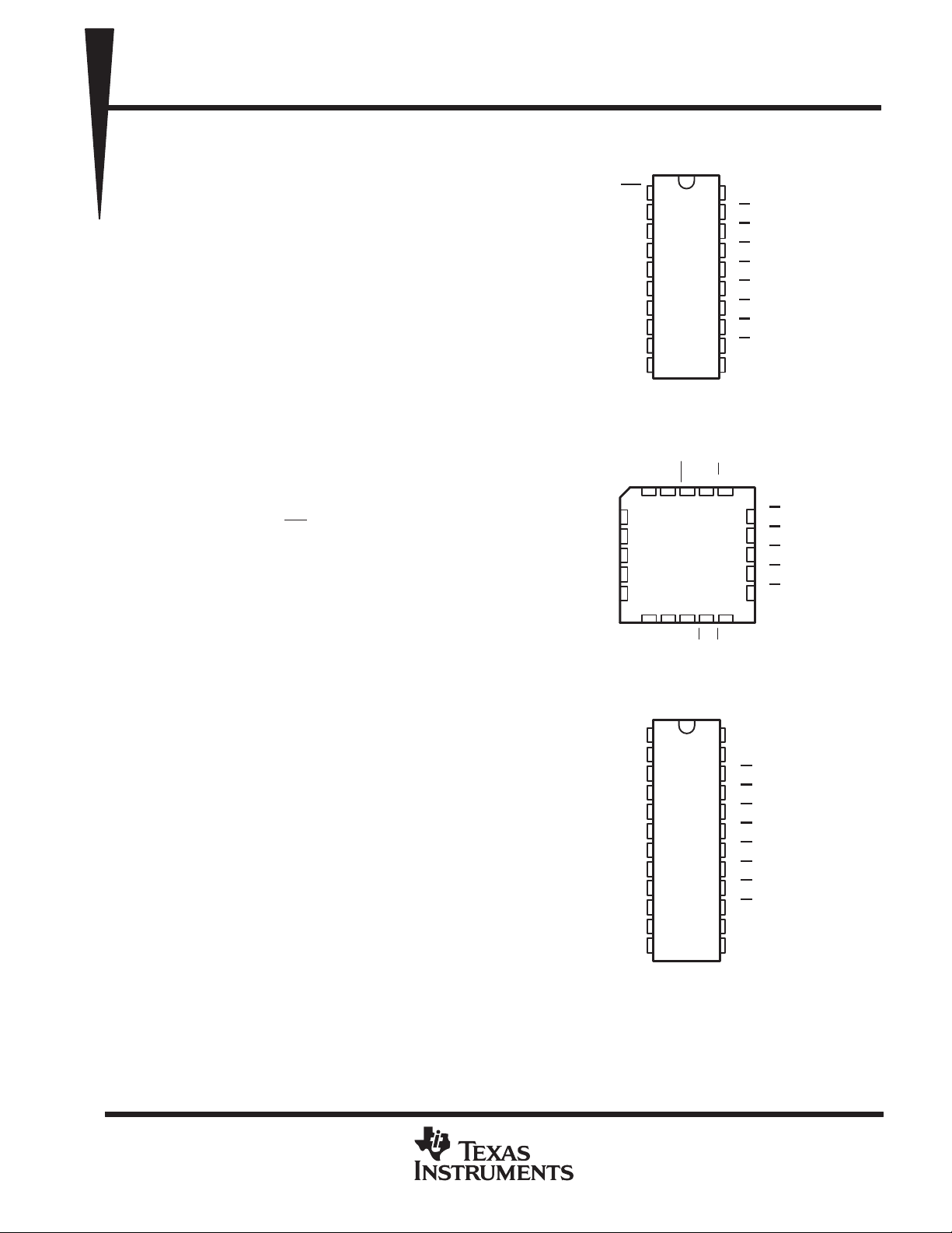
SN54ALS576B, SN54AS576 ...J OR W PACKAGE
SN74ALS576B, SN74AS576 . . . DW OR N PACKAGE
SN54ALS576B, SN54AS576 . . . FK PACKAGE
3D
4D
5D
6D
7D
SN74ALS577A . . . DW OR NT PACKAGE
(TOP VIEW)
OE
1
1D
2
2D
3
3D
4
4D
5
5D
6
6D
7
7D
8
9
8D
GND
10
(TOP VIEW)
2D1DOE
3212019
4
5
6
7
8
910111213
8D
(TOP VIEW)
GND
20
19
18
17
16
15
14
13
12
11
V
CLK
CC
8Q
V
CC
1Q
2Q
3Q
4Q
5Q
6Q
7Q
8Q
CLK
18
17
16
15
14
7Q 1Q
2Q
3Q
4Q
5Q
6Q
PRODUCTION DATA information is current as of publication date.
Products conform to specifications per the terms of Texas Instruments
standard warranty. Production processing does not necessarily include
testing of all parameters.
CLR
1
OE
2
1D
3
2D
4
3D
5
4D
6
5D
7
6D
8
7D
9
8D
10
NC
11
GND
12
NC – No internal connection
Copyright 1995, Texas Instruments Incorporated
24
23
22
21
20
19
18
17
16
15
14
13
V
CC
NC
1Q
2Q
3Q
4Q
5Q
6Q
7Q
8Q
CLK
NC
POST OFFICE BOX 655303 • DALLAS, TEXAS 75265
1
SN54ALS576B, SN54AS576
SN74ALS576B, SN74ALS577A, SN74AS576
OCTAL D-TYPE EDGE-TRIGGERED FLIP-FLOPS WITH 3-STATE OUTPUTS
SDAS065B – DECEMBER 1982 – REVISED JANUARY 1995
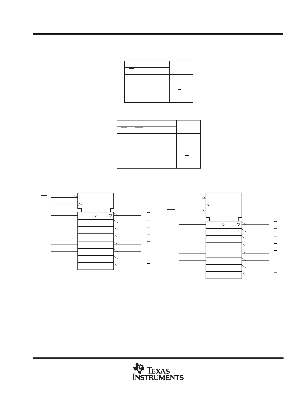
Function Tables
′ALS576B, ′AS576
(each flip-flop)
INPUTS
OE CLK D
L ↑ H L
L ↑ LH
LLX
HXX Z
SN74ALS577A
(each flip-flop)
INPUTS
OE CLR CLK D
L L ↑ X H
L H ↑ HL
LH↑LH
LHLX
HXXX Z
OUTPUT
Q
Q
0
OUTPUT
Q
Q
0
logic symbols
1
OE
11
CLK
2
1D
3
2D
4
3D
5
4D
6
5D
7
6D
8
7D
9
8D
†
These symbols are in accordance with ANSI/IEEE Std 91-1984 and
IEC Publication 617-12.
Pin numbers shown for the ′ALS576B and ′AS576 are for the DW,
J, N, and W packages.
†
′ALS576B, ′AS576 SN74ALS577A
EN
C1
1D
19
18
17
16
15
14
13
12
1Q
2Q
3Q
4Q
5Q
6Q
7Q
8Q
2
OE
14
CLK
1
CLR
3
1D
4
2D
5
3D
6
4D
7
5D
8
6D
9
7D
10
8D
Pin numbers shown for the SN74ALS577A are for the DW and NT
packages.
EN
1R
1D
C1
22
21
20
19
18
17
16
15
1Q
2Q
3Q
4Q
5Q
6Q
7Q
8Q
2
POST OFFICE BOX 655303 • DALLAS, TEXAS 75265
OCTAL D-TYPE EDGE-TRIGGERED FLIP-FLOPS WITH 3-STATE OUTPUTS
f
Clock frequenc
MH
twPulse duration
ns
t
S
CLK↑
ns
t
Hold ti
CLK↑
ns
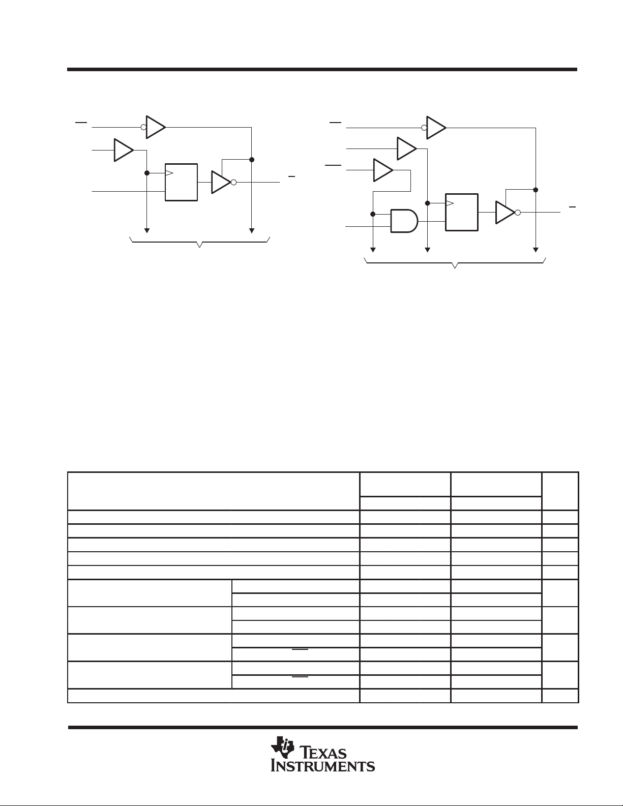
logic diagrams (positive logic)
′ALS576B, ′AS576 SN74ALS577A
SN54ALS576B, SN54AS576
SN74ALS576B, SN74ALS577A, SN74AS576
SDAS065B – DECEMBER 1982 – REVISED JANUARY 1995
1
OE
11
CLK
C1
2
1D
Pin numbers shown are for the DW, J, N, and W packages. Pin numbers shown are for the DW and NT packages.
1D
To Seven Other Channels
19
1Q
OE
CLK
CLR
1D
2
14
1
3
C1
1D
To Seven Other Channels
22
absolute maximum ratings over operating free-air temperature range (unless otherwise noted)
Supply voltage, V
Input voltage, V
Voltage applied to a disabled 3-state output 5.5 V. . . . . . . . . . . . . . . . . . . . . . . . . . . . . . . . . . . . . . . . . . . . . . . . . .
Operating free-air temperature range, T
Storage temperature range –65°C to 150°C. . . . . . . . . . . . . . . . . . . . . . . . . . . . . . . . . . . . . . . . . . . . . . . . . . . . . . .
†
Stresses beyond those listed under “absolute maximum ratings” may cause permanent damage to the device. These are stress ratings only, and
functional operation of the device at these or any other conditions beyond those indicated under “recommended operating conditions” is not
implied. Exposure to absolute-maximum-rated conditions for extended periods may affect device reliability.
7 V. . . . . . . . . . . . . . . . . . . . . . . . . . . . . . . . . . . . . . . . . . . . . . . . . . . . . . . . . . . . . . . . . . . . . . . .
CC
7 V. . . . . . . . . . . . . . . . . . . . . . . . . . . . . . . . . . . . . . . . . . . . . . . . . . . . . . . . . . . . . . . . . . . . . . . . . . . .
I
: SN54ALS576B –55°C to 125°C. . . . . . . . . . . . . . . . . . . . . . . . . . .
A
SN74ALS576B, SN74ALS577A 0°C to 70°C. . . . . . . . . . . . . . . . .
1Q
†
recommended operating conditions
V
CC
V
IH
V
IL
I
OH
I
OL
clock
su
h
T
A
Supply voltage 4.5 5 5.5 4.5 5 5.5 V
High-level input voltage 2 2 V
Low-level input voltage 0.7 0.8 V
High-level output current –1 –2.6 mA
Low-level output current 12 24 mA
y
etup time before
me after
Operating free-air temperature –55 125 0 70 °C
′ALS576B 0 22 0 30
SN74ALS577A
′ALS576B, CLK high or low 25 16.5
SN74ALS577A, CLK high or low 16.5
Data 15 15
SN74ALS577A CLR 15
Data 4 0
SN74ALS577A CLR 0
SN54ALS576B
MIN NOM MAX MIN NOM MAX
SN74ALS576B
SN74ALS577A
0 30
UNIT
z
POST OFFICE BOX 655303 • DALLAS, TEXAS 75265
3

SN54ALS576B, SN54AS576
V
V
V
V
4.5 V
V
CLK
A
Q
ns
OE
A
Q
ns
OE
A
Q
ns
SN74ALS576B, SN74ALS577A, SN74AS576
OCTAL D-TYPE EDGE-TRIGGERED FLIP-FLOPS WITH 3-STATE OUTPUTS
SDAS065B – DECEMBER 1982 – REVISED JANUARY 1995
electrical characteristics over recommended operating free-air temperature range (unless
otherwise noted)
PARAMETER TEST CONDITIONS
V
IK
V
OH
OL
I
OZH
I
OZL
I
I
I
IH
I
IL
‡
I
O
I
CC
†
All typical values are at VCC = 5 V, TA = 25°C.
‡
The output conditions have been chosen to produce a current that closely approximates one half of the true short-circuit output current, IOS.
VCC = 4.5 V, II = –18 mA –1.2 –1.2 V
VCC = 4.5 V to 5.5 V, IOH = –0.4 mA VCC –2 VCC –2
= 4.5
CC
=
CC
VCC = 5.5 V, VO = 2.7 V 20 20 µA
VCC = 5.5 V, VO = 0.4 V –20 –20 µA
VCC = 5.5 V, VI = 7 V 0.1 0.1 mA
VCC = 5.5 V, VI = 2.7 V 20 20 µA
VCC = 5.5 V, VI = 0.4 V –0.2 –0.2 mA
VCC = 5.5 V, VO = 2.25 V –20 –112 –30 –112 mA
VCC = 5.5 V
IOH = –1 mA 2.4 3.3
IOH = –2.6 mA 2.4 3.2
IOL = 12 mA 0.25 0.4 0.25 0.4
IOL = 24 mA 0.35 0.5
Outputs high 10 18 10 18
Outputs low 15 24 15 24
Outputs disabled 16 30 16 30
SN54ALS576B
MIN TYP†MAX MIN TYP†MAX
SN74ALS576B
SN74ALS577A
UNIT
V
mA
switching characteristics (see Figure 1)
VCC = 4.5 V to 5.5 V,
CL = 50 pF,
PARAMETER
f
max
t
PLH
t
PHL
t
PZH
t
PZL
t
PHZ
t
§
For conditions shown as MIN or MAX, use the appropriate value specified under recommended operating conditions.
PLZ
FROM
(INPUT)
TO
(OUTPUT)
ny
ny
ny
SN54ALS576B SN74ALS576B SN74ALS577A
MIN MAX MIN MAX MIN MAX
22 30 30 MHz
4 24 3 14 4 14
4 20 4 14 4 14
4 24 3 18 4 18
3 23 4 18 4 18
2 14 1 10 2 10
3 29 2 15 3 15
R1 = 500 Ω
R2 = 500 Ω,
TA = MIN to MAX
,
§
UNIT
4
POST OFFICE BOX 655303 • DALLAS, TEXAS 75265

SN54ALS576B, SN54AS576
UNIT
tw*
Pulse duration
ns
SN74ALS576B, SN74ALS577A, SN74AS576
OCTAL D-TYPE EDGE-TRIGGERED FLIP-FLOPS WITH 3-STATE OUTPUTS
SDAS065B – DECEMBER 1982 – REVISED JANUARY 1995
absolute maximum ratings over operating free-air temperature range (unless otherwise noted)
Supply voltage, V
Input voltage, V
Voltage applied to a disabled 3-state output 5.5 V. . . . . . . . . . . . . . . . . . . . . . . . . . . . . . . . . . . . . . . . . . . . . . . . . .
Operating free-air temperature range, T
Storage temperature range –65°C to 150°C. . . . . . . . . . . . . . . . . . . . . . . . . . . . . . . . . . . . . . . . . . . . . . . . . . . . . . .
†
Stresses beyond those listed under “absolute maximum ratings” may cause permanent damage to the device. These are stress ratings only, and
functional operation of the device at these or any other conditions beyond those indicated under “recommended operating conditions” is not
implied. Exposure to absolute-maximum-rated conditions for extended periods may affect device reliability.
7 V. . . . . . . . . . . . . . . . . . . . . . . . . . . . . . . . . . . . . . . . . . . . . . . . . . . . . . . . . . . . . . . . . . . . . . . .
CC
7 V. . . . . . . . . . . . . . . . . . . . . . . . . . . . . . . . . . . . . . . . . . . . . . . . . . . . . . . . . . . . . . . . . . . . . . . . . . . .
I
: SN54AS576 –55°C to 125°C. . . . . . . . . . . . . . . . . . . . . . . . . . . . . .
A
SN74AS576 0°C to 70°C. . . . . . . . . . . . . . . . . . . . . . . . . . . . . . . . . .
recommended operating conditions
SN54AS576 SN74AS576
MIN NOM MAX MIN NOM MAX
V
CC
V
IH
V
IL
I
OH
I
OL
f
clock
tsu* Setup time, data before CLK↑ 3 2 ns
th* Hold time, data after CLK↑ 3 2 ns
T
A
* On products compliant to MIL-STD-883, Class B, this parameter is based on characterization data but is not production tested.
Supply voltage 4.5 5 5.5 4.5 5 5.5 V
High-level input voltage 2 2 V
Low-level input voltage 0.8 0.8 V
High-level output current –12 –15 mA
Low-level output current 32 48 mA
* Clock frequency 0 100 0 125 MHz
*
Operating free-air temperature –55 125 0 70 °C
CLK high 5 4
CLK low 4 2
†
POST OFFICE BOX 655303 • DALLAS, TEXAS 75265
5

SN54ALS576B, SN54AS576
PARAMETER
TEST CONDITIONS
UNIT
V
V
VOLV
V
V
I
V
V
V
mA
CLK
A
Q
ns
OE
A
Q
ns
OE
A
Q
ns
SN74ALS576B, SN74ALS577A, SN74AS576
OCTAL D-TYPE EDGE-TRIGGERED FLIP-FLOPS WITH 3-STATE OUTPUTS
SDAS065B – DECEMBER 1982 – REVISED JANUARY 1995
electrical characteristics over recommended operating free-air temperature range (unless
otherwise noted)
SN54AS576 SN74AS576
MIN TYP†MAX MIN TYP†MAX
V
IK
V
OH
I
OZH
I
OZL
I
I
I
IH
IL
I
O
I
CC
†
All typical values are at VCC = 5 V, TA = 25°C.
‡
The output conditions have been chosen to produce a current that closely approximates one half of the true short-circuit output current, IOS.
D
All others
‡
VCC = 4.5 V, II = –18 mA –1.2 –1.2 V
VCC = 4.5 V to 5.5 V, IOH = –2 mA VCC –2 VCC –2
= 4.5
CC
= 4.5
CC
VCC = 5.5 V, VO = 2.7 V 50 50 µA
VCC = 5.5 V, VO = 0.4 V –50 –50 µA
VCC = 5.5 V, VI = 7 V 0.1 0.1 mA
VCC = 5.5 V, VI = 2.7 V 20 20 µA
= 5.5 V,
CC
VCC = 5.5 V, VO = 2.25 V –30 –112 –30 –112 mA
VCC = 5.5 V
IOH = –12 mA 2.4 3.2
IOH = –15 mA 2.4 3.3
IOL = 32 mA 0.29 0.5
IOL = 48 mA 0.33 0.5
= 0.4
I
Outputs high 77 125 77 125
Outputs low 84 135 84 135
Outputs disabled 84 135 84 135
–3 –2
–0.5 –0.5
V
mA
switching characteristics (see Figure 1)
VCC = 4.5 V to 5.5 V,
CL = 50 pF,
PARAMETER
f
* 100 125 MHz
max
t
PLH
t
PHL
t
PZH
t
PZL
t
PHZ
t
PLZ
* On products compliant to MIL-STD-883, Class B, this parameter is based on characterization data but is not production tested.
§
For conditions shown as MIN or MAX, use the appropriate value specified under recommended operating conditions.
FROM
(INPUT)
TO
(OUTPUT)
ny
ny
ny
R1 = 500 Ω
R2 = 500 Ω,
TA = MIN to MAX
SN54AS576 SN74AS576
MIN MAX MIN MAX
3 11 3 8
4 11 4 9
2 7 2 6
3 11 3 10
2 7 2 6
2 7 2 6
,
§
UNIT
6
POST OFFICE BOX 655303 • DALLAS, TEXAS 75265

From Output
Under Test
(see Note A)
SN54ALS576B, SN54AS576
SN74ALS576B, SN74ALS577A, SN74AS576
OCTAL D-TYPE EDGE-TRIGGERED FLIP-FLOPS WITH 3-STATE OUTPUTS
SDAS065B – DECEMBER 1982 – REVISED JANUARY 1995
PARAMETER MEASUREMENT INFORMATION
SERIES 54ALS/74ALS AND 54AS/74AS DEVICES
7 V
V
CC
S1
R
L
Test
Point
C
L
R
L
From Output
Under Test
(see Note A)
Test
Point
C
L
From Output
Under Test
(see Note A)
R1
C
L
RL = R1 = R2
Test
Point
R2
LOAD CIRCUIT FOR
BI-STATE
TOTEM-POLE OUTPUTS
Timing
Input
t
su
Data
Input
VOLTAGE WAVEFORMS
SETUP AND HOLD TIMES
Output
Control
(low-level
enabling)
Waveform 1
S1 Closed
(see Note B)
Waveform 2
S1 Open
(see Note B)
t
PZL
t
PZH
ENABLE AND DISABLE TIMES, 3-STATE OUTPUTS
VOLTAGE WAVEFORMS
1.3 V
t
PHZ
1.3 V
1.3 V
t
1.3 V1.3 V
1.3 V1.3 V
FOR OPEN-COLLECTOR OUTPUTS
h
t
PLZ
LOAD CIRCUIT
3.5 V
0.3 V
3.5 V
0.3 V
3.5 V
0.3 V
[
3.5 V
V
OL
0.3 V
V
OH
0.3 V
[
0 V
High-Level
Low-Level
Out-of-Phase
(see Note C)
Pulse
Pulse
Input
In-Phase
Output
Output
LOAD CIRCUIT
FOR 3-STATE OUTPUTS
1.3 V 1.3 V
t
w
1.3 V 1.3 V
VOLTAGE WAVEFORMS
PULSE DURATIONS
1.3 V 1.3 V
t
PLH
t
PHL
1.3 V 1.3 V
VOLTAGE WAVEFORMS
PROPAGATION DELAY TIMES
1.3 V1.3 V
t
PHL
t
PLH
3.5 V
0.3 V
3.5 V
0.3 V
3.5 V
0.3 V
V
V
V
V
OH
OL
OH
OL
NOTES: A. CL includes probe and jig capacitance.
B. Waveform 1 is for an output with internal conditions such that the output is low except when disabled by the output control.
Waveform 2 is for an output with internal conditions such that the output is high except when disabled by the output control.
C. When measuring propagation delay items of 3-state outputs, switch S1 is open.
D. All input pulses have the following characteristics: PRR ≤ 1 MHz, tr = tf = 2 ns, duty cycle = 50%.
E. The outputs are measured one at a time with one transition per measurement.
Figure 1. Load Circuits and Voltage Waveforms
POST OFFICE BOX 655303 • DALLAS, TEXAS 75265
7

IMPORTANT NOTICE
T exas Instruments and its subsidiaries (TI) reserve the right to make changes to their products or to discontinue
any product or service without notice, and advise customers to obtain the latest version of relevant information
to verify, before placing orders, that information being relied on is current and complete. All products are sold
subject to the terms and conditions of sale supplied at the time of order acknowledgement, including those
pertaining to warranty, patent infringement, and limitation of liability.
TI warrants performance of its semiconductor products to the specifications applicable at the time of sale in
accordance with TI’s standard warranty. Testing and other quality control techniques are utilized to the extent
TI deems necessary to support this warranty . Specific testing of all parameters of each device is not necessarily
performed, except those mandated by government requirements.
CERT AIN APPLICATIONS USING SEMICONDUCTOR PRODUCTS MAY INVOLVE POTENTIAL RISKS OF
DEATH, PERSONAL INJURY, OR SEVERE PROPERTY OR ENVIRONMENTAL DAMAGE (“CRITICAL
APPLICATIONS”). TI SEMICONDUCTOR PRODUCTS ARE NOT DESIGNED, AUTHORIZED, OR
WARRANTED TO BE SUITABLE FOR USE IN LIFE-SUPPORT DEVICES OR SYSTEMS OR OTHER
CRITICAL APPLICA TIONS. INCLUSION OF TI PRODUCTS IN SUCH APPLICATIONS IS UNDERST OOD TO
BE FULLY AT THE CUSTOMER’S RISK.
In order to minimize risks associated with the customer’s applications, adequate design and operating
safeguards must be provided by the customer to minimize inherent or procedural hazards.
TI assumes no liability for applications assistance or customer product design. TI does not warrant or represent
that any license, either express or implied, is granted under any patent right, copyright, mask work right, or other
intellectual property right of TI covering or relating to any combination, machine, or process in which such
semiconductor products or services might be or are used. TI’s publication of information regarding any third
party’s products or services does not constitute TI’s approval, warranty or endorsement thereof.
Copyright 1998, Texas Instruments Incorporated
 Loading...