

Texas Instruments SN74ACT7805-25DLR, SN74ACT7805-40DL, SN74ACT7805-40DLR, SN74ACT7805-15DL, SN74ACT7805-15DLR Datasheet
...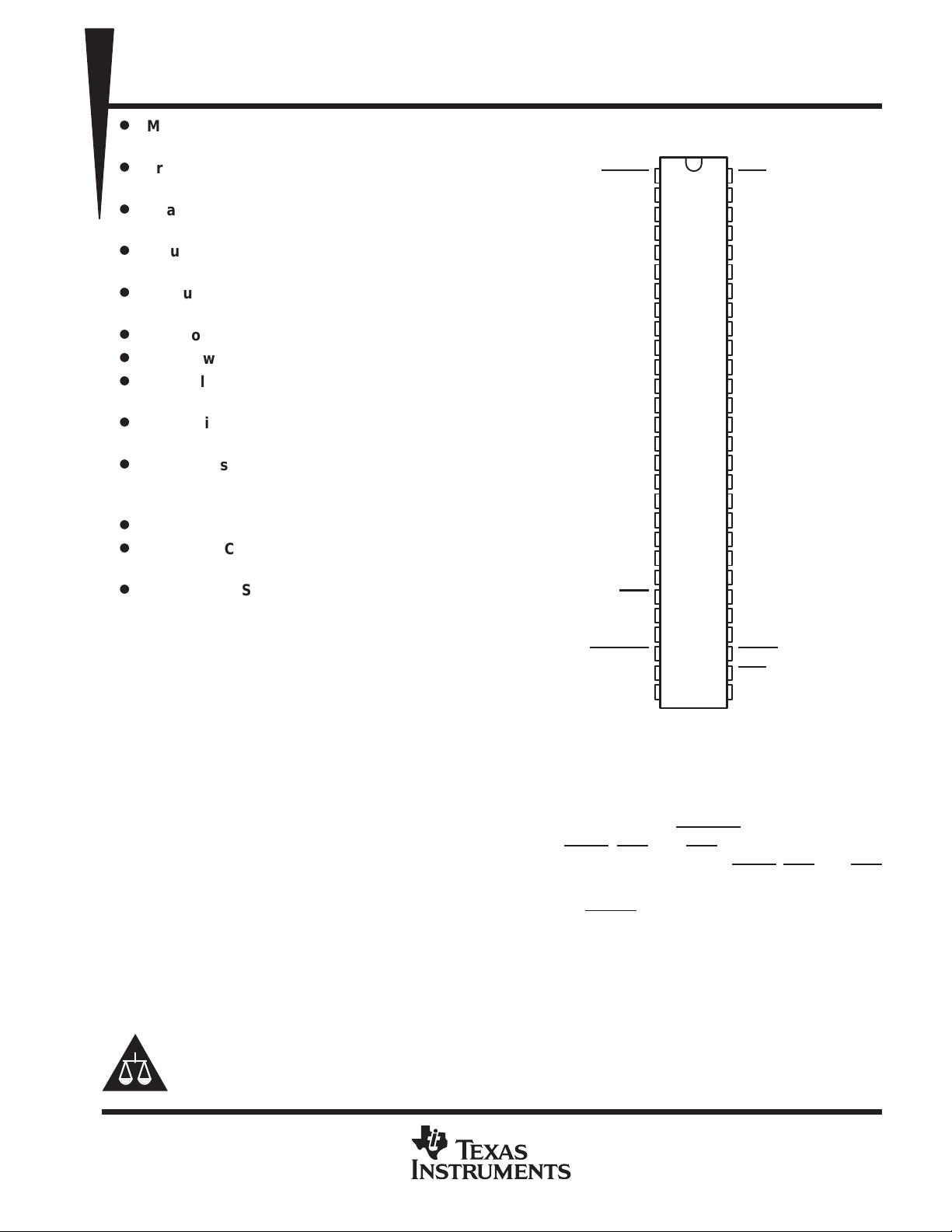
SN74ACT7805
256 × 18 CLOCKED FIRST-IN, FIRST-OUT MEMORY
SCAS201B – MARCH 1991 – REVISED APRIL 1998
D17
D16
D15
D14
D13
D12
D1 1
D10
V
CC
D9
D8
GND
D7
D6
D5
D4
D3
D2
D1
D0
HF
PEN
AF/AE
IR
DL PACKAGE
(TOP VIEW)
1
56
2
55
3
54
4
53
5
52
6
51
7
50
8
49
9
48
10
47
11
46
12
45
13
44
14
43
15
42
16
41
17
40
18
39
19
38
20
37
21
36
22
35
23
34
24
33
25
32
26
31
27
30
28
29
OE1
Q17
Q16
Q15
GND
Q14
V
CC
Q13
Q12
Q11
Q10
Q9
GND
Q8
Q7
Q6
Q5
V
CC
Q4
Q3
Q2
GND
Q1
Q0
RDCLK
RDEN
OE2
OR
D
Member of the Texas Instruments
Widebus Family
D
Free-Running Read and Write Clocks Can
Be Asynchronous or Coincident
D
Read and Write Operations Synchronized
to Independent System Clocks
D
Input-Ready Flag Synchronized to Write
Clock
D
Output-Ready Flag Synchronized to Read
Clock
D
256 Words by 18 Bits
D
Low-Power Advanced CMOS Technology
D
Half-Full Flag and Programmable
Almost-Full/Almost-Empty Flag
D
Bidirectional Configuration and Width
Expansion Without Additional Logic
D
Fast Access Times of 12 ns With a 50-pF
Load and All Data Outputs Switching
Simultaneously
D
Data Rates up to 67 MHz
D
Pin-to-Pin Compatible With SN74ACT7803
and SN74ACT7813
D
Packaged in Shrink Small-Outline 300-mil
Package Using 25-mil Center-to-Center
Spacing
description
The SN74ACT7805 is a 256-word ×18-bit clocked
RESET
WRTCLK
WRTEN2
WRTEN1
FIFO suited for buffering asynchronous data
paths up to 67-MHz clock rates and 12-ns access
times. Two devices can be configured for bidirectional data buf fering without additional logic. Multiple distributed
V
and GND pins, along with Texas Instruments patented output edge control (OEC) circuit, dampen
CC
simultaneous switching noise.
The write clock (WRTCLK) and read clock (RDCLK) are free running and can be asynchronous or coincident.
Data is written to memory on the rising edge of WRTCLK when WRTEN1 is high, WRTEN2
Data is read from memory on the rising edge of RDCLK when RDEN
, OE1, and OE2 are low and OR is high.
The first word written to memory is clocked through to the output buffer , regardless of the RDEN
is low, and IR is high.
, OE1, and OE2
levels. The OR flag indicates that valid data is present on the output buffer.
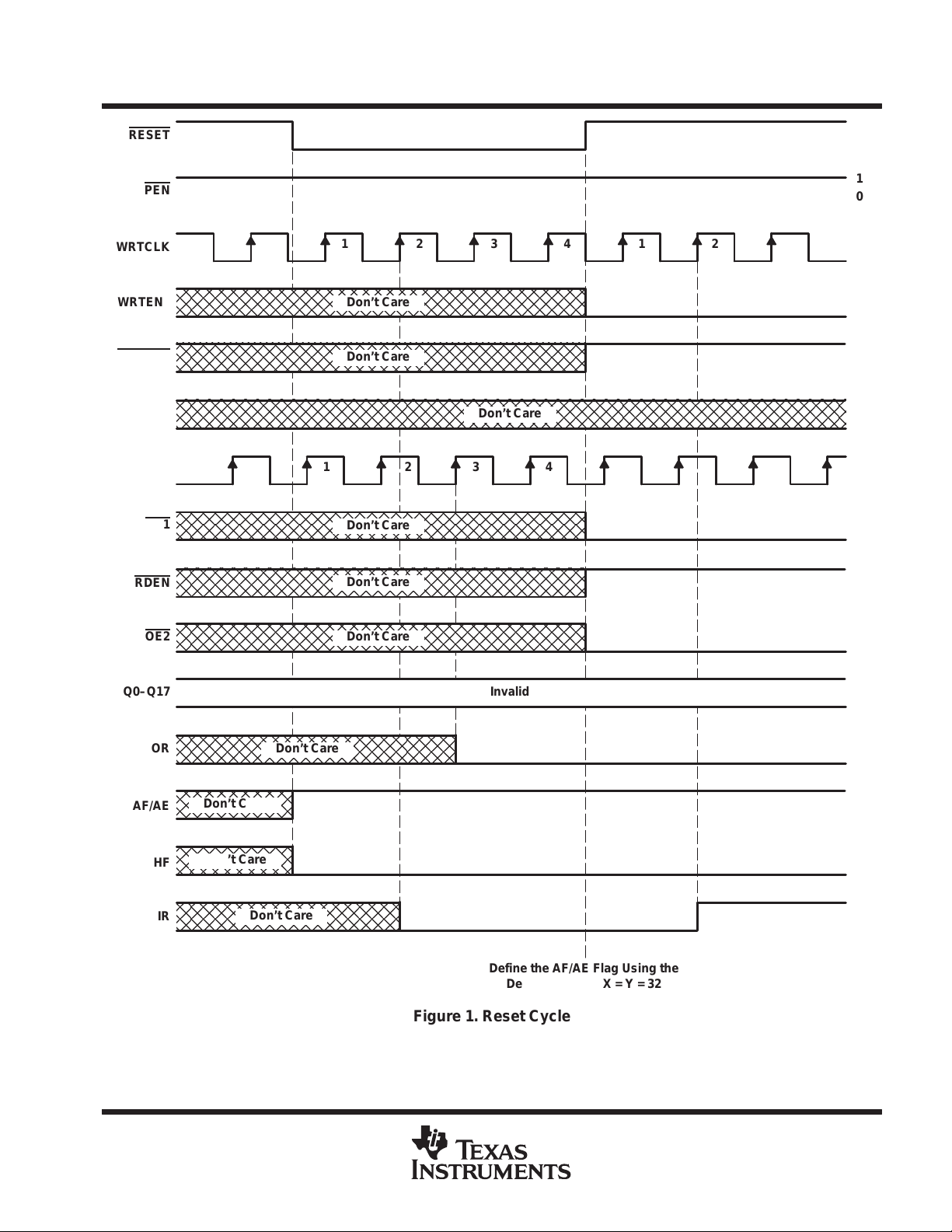
The FIFO can be reset asynchronously to WRTCLK and RDCLK. RESET
must be asserted while at least four
WRTCLK and four RDCLK rising edges occur to clear the synchronizing registers. Resetting the FIFO initializes
the input-ready (IR), output-ready (OR), and half-full (HF) flags low and the almost-full/almost-empty (AF/AE)
flag high. The FIFO must be reset upon power up.
The SN74ACT7805 is characterized for operation from 0°C to 70°C.
Please be aware that an important notice concerning availability, standard warranty, and use in critical applications of
Texas Instruments semiconductor products and disclaimers thereto appears at the end of this data sheet.
Widebus and OEC are trademarks of Texas Instruments Incorporated.
PRODUCTION DATA information is current as of publication date.
Products conform to specifications per the terms of Texas Instruments
standard warranty. Production processing does not necessarily include
testing of all parameters.
POST OFFICE BOX 655303 • DALLAS, TEXAS 75265
Copyright 1998, Texas Instruments Incorporated
1
SN74ACT7805
256 × 18 CLOCKED FIRST-IN, FIRST-OUT MEMORY
SCAS201B – MARCH 1991 – REVISED APRIL 1998
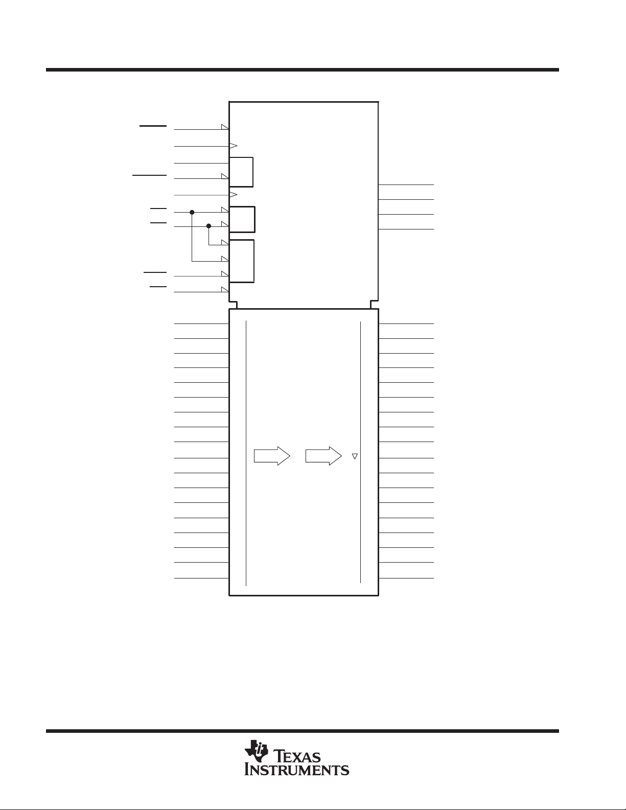
logic symbol
†
RESET
WRTCLK
WRTEN1
WRTEN2
RDCLK
OE1
OE2
RDEN
PEN
D0
D1
D2
D3
D4
D5
D6
D7
D8
D9
D10
D11
D12
D13
D14
D15
D16
D17
1
25
27
26
32
56
30
31
23
21
20
19
18
17
16
15
14
12
11
9
8
7
6
5
4
3
2
Φ
FIFO 256 × 18
RESET
WRTCLK
&
RDCLK
&
&
PROGRAM ENABLE
0
17
SN74ACT7805
WRTEN
ALMOST FULL/EMPTY
EN1
RDEN
Data
HALF-FULL
Data
IN RDY
OUT RDY
1
17
28
IR
22
HF
24
AF/AE
29
OR
33
0
34
36
37
38
40
41
42
43
45
46
47
48
49
51
53
54
55
Q0
Q1
Q2
Q3
Q4
Q5
Q6
Q7
Q8
Q9
Q10
Q11
Q12
Q13
Q14
Q15
Q16
Q17
†
This symbol is in accordance with ANSI/IEEE Std 91-1984 and IEC Publication 617-12.
2
POST OFFICE BOX 655303 • DALLAS, TEXAS 75265
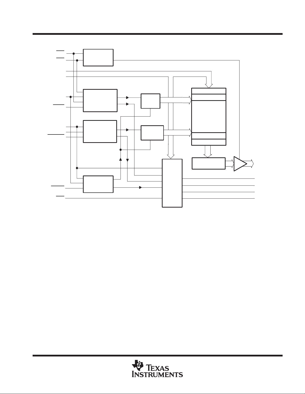
functional block diagram
SN74ACT7805
256 × 18 CLOCKED FIRST-IN, FIRST-OUT MEMORY
SCAS201B – MARCH 1991 – REVISED APRIL 1998
OE1
OE2
D0–D17
RDCLK
RDEN
WRTCLK
WRTEN1
WRTEN2
RESET
PEN
Output
Control
Synchronous
Read
Control
Synchronous
Write
Control
Reset
Logic
Read
Pointer
Write
Pointer
Status-
Flag
Logic
Location 1
Location 2
256 × 18 RAM
Location 255
Location 256
Register
Q0–Q17
OR
IR
HF
AF/AE
POST OFFICE BOX 655303 • DALLAS, TEXAS 75265
3
SN74ACT7805
I/O
DESCRIPTION
256 × 18 CLOCKED FIRST-IN, FIRST-OUT MEMORY
SCAS201B – MARCH 1991 – REVISED APRIL 1998
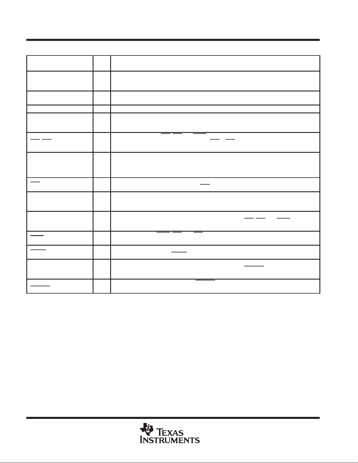
Terminal Functions
TERMINAL
NAME NO.
Almost-full/almost-empty flag. Depth offset values can be programmed for AF/AE, or the default
AF/AE 24 O
D0–D17
HF 22 O Half-full flag. HF is high when the FIFO memory contains 128 or more words. HF is low after reset.
IR 28 O
OE1, OE2 56, 30 I
OR 29 O
PEN
Q0–Q17
RDCLK 32 I
RDEN
RESET
WRTCLK 25 I
WRTEN1,
WRTEN2
21–14, 12–1 1,
9–2
23 I
33–34, 36–38,
40–43, 45–49,
51, 53–55
31 I
1 I
27, 26 I
value of 32 can be used for both the almost-empty offset (X) and the almost-full offset (Y). AF/AE is
high when memory contains X or fewer words or (256 – Y) or more words. AF/AE is high after reset.
I 18-bit data input port
Input-ready flag. IR is synchronized to the low-to-high transition of WRTCLK. When IR is low, the
FIFO is full and writes are disabled. IR is low during reset and goes high on the second low-to-high
transition of WRTCLK after reset.
Output enables. When OE1, OE2, and RDEN are low and OR is high, data is read from the FIFO on
a low-to-high transition of RDCLK. When either OE1
outputs are in the high-impedance state.
Output-ready flag. OR is synchronized to the low-to-high transition of RDCLK. When OR is low, the
FIFO is empty and reads are disabled. Ready data is present on Q0–Q17 when OR is high. OR is
low during reset and goes high on the third low-to-high transition of RDCLK after the first word is
loaded to empty memory .
Program enable. After reset and before the first word is written to the FIFO, the binary value on D0–D6
is latched as an AF/AE offset value when PEN
18-bit data output port. After the first valid write to empty memory , the first word is output on Q0–Q17
on the third rising edge of RDCLK. OR also is asserted high at this time to indicate ready data. When
O
OR is low, the last word read from the FIFO is present on Q0–Q17.
Read clock. RDCLK is a continuous clock and can be asynchronous or coincident to WRTCLK. A
low-to-high transition of RDCLK reads data from memory when OE1
OR is high. OR is synchronous to the low-to-high transition or RDCLK.
Read enable. When RDEN, OE1, and OE2 are low and OR is high, data is read from the FIFO on
the low-to-high transition of RDCLK.
Reset. To reset the FIFO, four low-to-high transitions of RDCLK and four low-to-high transitions of
WRTCLK must occur while RESET
Write clock. WRTCLK is a continuous clock and can be asynchronous or coincident to RDCLK. A
low-to-high transition of WRTCLK writes data to memory when WRTEN2
and IR is high. IR is synchronous to the low-to-high transition of WRTCLK.
Write enables. When WRTEN1 is high, WRTEN2 is low, and IR is high, data is written to the FIFO
on a low-to-high transition of WRTCLK.
is low. This sets HF, IR, and OR low and AF/AE high.
or OE2 is high, reads are disabled and the data
is low and WRTCLK is high.
, OE2, and RDEN are low and
is low, WRTEN1 is high,
4
POST OFFICE BOX 655303 • DALLAS, TEXAS 75265
SN74ACT7805
256 × 18 CLOCKED FIRST-IN, FIRST-OUT MEMORY
SCAS201B – MARCH 1991 – REVISED APRIL 1998
RESET
PEN
WRTCLK
WRTEN1
WRTEN2
D0–D17
RDCLK
OE1
RDEN
1
0
123412
Don’t Care
Don’t Care
Don’t Care
1234
Don’t Care
Don’t Care
OE2
Q0–Q17
OR
AF/AE
HF
IR
Don’t Care
Invalid
Don’t Care
Don’t Care
Don’t Care
Don’t Care
Define the AF/AE Flag Using the
Default Value of X = Y = 32
Figure 1. Reset Cycle
POST OFFICE BOX 655303 • DALLAS, TEXAS 75265
5
 Loading...