

SN74ACT1071
10-BIT BUS-TERMINATION ARRAY
WITH BUS-HOLD FUNCTION
SCAS192 – D3994, MARCH 1992 – REVISED APRIL 1993
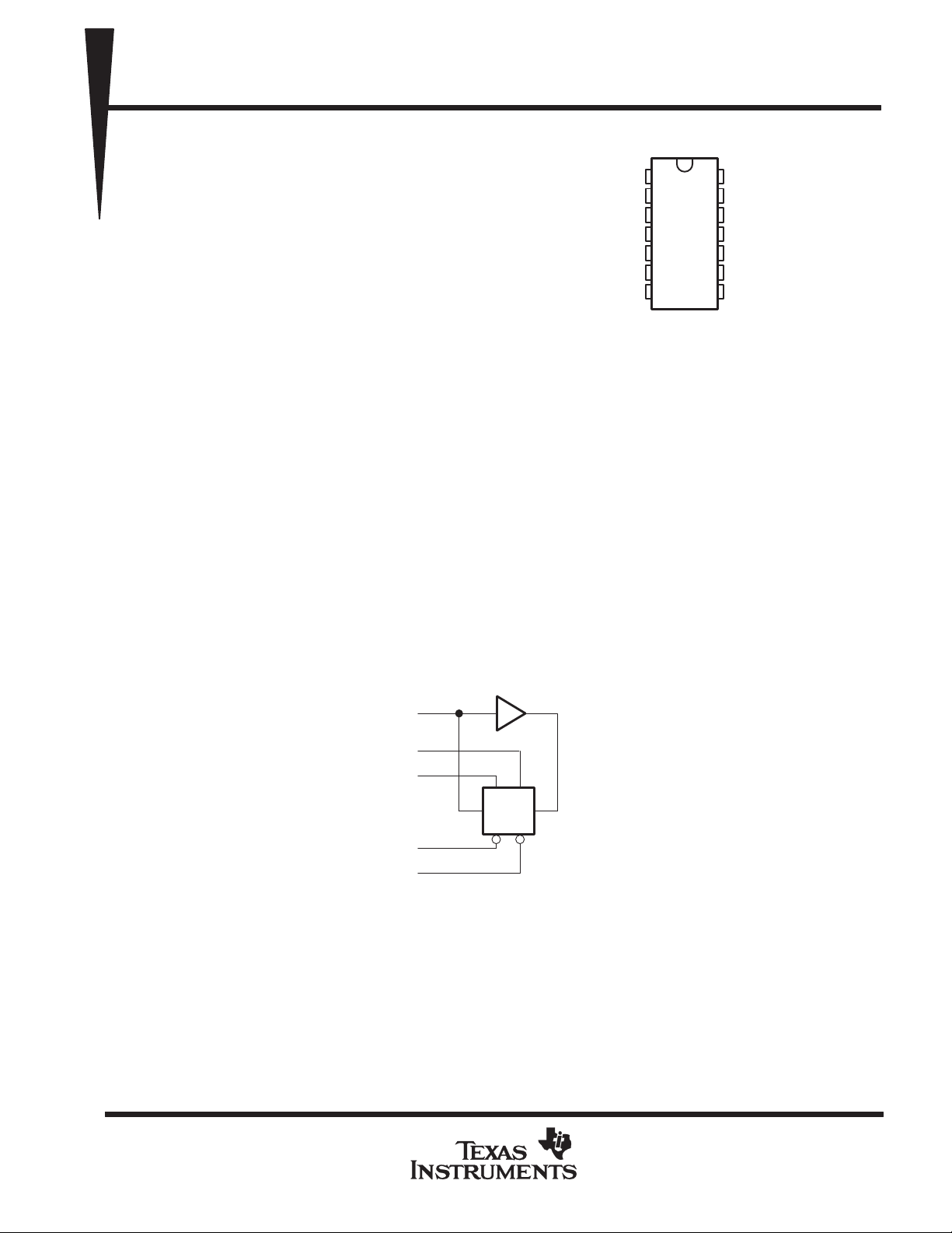
D1
D2
GND
GND
D3
D4
D5
D PACKAGE
(TOP VIEW)
14
1
13
2
12
3
11
4
10
5
6
7
9
8
D10
D9
D8
V
CC
V
CC
D7
D6
• Designed to Ensure Defined Voltage Levels
on Floating Bus Lines in CMOS Systems
• Reduces Undershoot and Overshoot
Caused By Line Reflections
• Repetitive Peak Forward
Current ...I
FRM
= 100 mA
• Inputs Are TTL-Voltage Compatible
• Low Power Consumption (Like CMOS)
• ESD Protection Exceeds 2000 V Per
MIL-STD-883C, Method 3015; Exceeds
200 V Using Machine Model
(C = 200 pF, R = 0)
• Center-Pin V
Minimizes High-Speed Switching Noise
and GND Configuration
CC
description
This device is designed to terminate bus lines in CMOS systems. The integrated low-impedance diodes clamp
the voltage of undershoots and overshoots caused by line reflections and ensure signal integrity. The device
also contains a bus-hold function that consists of a CMOS-buffer stage with a high-resistance feedback path
between its output and its input. The SN74ACT1071 prevents bus lines from floating without using pullup or
pulldown resistors.
The high-impedance inputs of these internal buffers are connected to the input terminals of the device. The
feedback path on each internal buffer stage keeps a bus line tied to the bus holder at the last valid logic state
generated by an active driver before the bus switches to the high-impedance state.
The SN74ACT1071 is characterized for operation from –40°C to 85°C.
logic diagram, one of ten channels (positive logic)
1
D1
11
V
CC
10
V
CC
TG
3
GND
4
GND
PRODUCTION DATA information is current as of publication date.
Products conform to specifications per the terms of Texas Instruments
standard warranty. Production processing does not necessarily include
testing of all parameters.
POST OFFICE BOX 655303 • DALLAS, TEXAS 75265
Copyright 1993, Texas Instruments Incorporated
4–1
SN74ACT1071
PARAMETER
TEST CONDITIONS
MIN
MAX
UNIT
10-BIT BUS-TERMINATION ARRAY
WITH BUS-HOLD FUNCTION
SCAS192 – D3994, MARCH 1992 – REVISED APRIL 1993
absolute maximum ratings over operating free-air temperature range (unless otherwise noted)
†
Supply voltage range, VCC –0.5 V to 7 V. . . . . . . . . . . . . . . . . . . . . . . . . . . . . . . . . . . . . . . . . . . . . . . . . . . . . . . . . .
Input voltage range, VI (see Note 1) –0.5 V to VCC + 0.5 V. . . . . . . . . . . . . . . . . . . . . . . . . . . . . . . . . . . . . . . . .
Continuous input clamp current, I
Positive-peak input clamp current, I
Negative-peak input clamp current, I
(V
< 0 or VI > VCC) ±20 mA. . . . . . . . . . . . . . . . . . . . . . . . . . . . . . . . . . . .
IK
I
(VI > VCC) (tw < 1 µs, duty cycle < 20%) 100 mA. . . . . . . . . . . . . . . . .
IK
(V
< 0) (tw < 1 µs, duty cycle < 20%) –100 mA. . . . . . . . . . . . . . . . . .
IK
I
Storage temperature range –65°C to 150°C. . . . . . . . . . . . . . . . . . . . . . . . . . . . . . . . . . . . . . . . . . . . . . . . . . . . . . .
†
Stresses beyond those listed under “absolute maximum ratings” may cause permanent damage to the device. These are stress ratings only, and
functional operation of the device at these or any other conditions beyond those indicated under “recommended operating conditions” is not
implied. Exposure to absolute-maximum-rated conditions for extended periods may affect device reliability.
NOTE 1: The input negative-voltage rating may be exceeded if the input clamp-current rating is observed.
recommended operating conditions
MIN MAX UNIT
V
CC
V
IH
V
IL
V
I
T
A
Supply voltage 4.5 5.5 V
High-level input voltage 2.5 V
Low-level input voltage 0.8 V
Input voltage 0 V
Operating free-air temperature –40 85 °C
CC
V
electrical characteristics over recommended operating free-air temperature range (unless
otherwise noted)
TA = 25°C
MIN TYP
I
IL
I
IH
V
IKL
V
IKH
‡
I
CC
∆I
CC
C
i
†
All typical values are at VCC = 5 V.
‡
Inputs may be set high or low prior to the ICC measurement.
§
This is the increase in supply current for each input that is at one of the specified TTL voltage levels rather than 0 V or VCC.
VCC = 4.5 to 5.5 V, VI = 0.8 V 0.15 0.3 0.9 0.1 1 mA
VCC = 4.5 to 5.5 V, VI = 2.5 V –0.2 –0.5 –1.4 –0.15 –1.5 mA
IIN = –18 mA –1.5 –1.5 V
IIN = 18 mA VCC+2 VCC+2 V
VCC = 5.5 V, Inputs open 4 40 µA
§
One input at 3.4 V , Other inputs at VCC or GND 0.9 1 mA
VI = VCC or GND 3 pF
†
MAX
4–2
POST OFFICE BOX 655303 • DALLAS, TEXAS 75265

10-BIT BUS-TERMINATION ARRAY
SCAS192 – D3994, MARCH 1992 – REVISED APRIL 1993
TYPICAL CHARACTERISTICS
SN74ACT1071
WITH BUS-HOLD FUNCTION
FORWARD CURRENT
INPUT VOLTAGE
(UPPER CLAMPING DIODE)
60
55
50
45
40
35
30
25
20
F
I – Forward Current – mA
15
10
5
0
5.5 6 6.5 7 7.5
VI – Input Voltage – V VI – Input Voltage – V
FORWARD CURRENT
vs
vs
INPUT VOLTAGE
(LOWER CLAMPING DIODE)
5
0
– 5
– 10
– 15
– 20
– 25
– 30
– 35
F
– 40
I – Forward Current – mA
– 45
– 50
– 55
8 8.5 9
– 60
–2 –1.75 –1.5 –1.25 –1 – 0.75
Figure 1 Figure 2
– 0.5 – 0.25 0
1
0.8
0.6
0.4
0.2
0
– 0.2
– 0.4
I
I – Input Current – mA
– 0.6
– 0.8
–1
01 23
INPUT CURRENT
vs
INPUT VOLTAGE
5
4.5
4
3.5
3
2.5
2
1.5
CC
I – Supply Current – mA
1
0.5
0
0123
456
VI – Input Voltage – V VI – Input Voltage – V
0.5 1.5 2.5 3.5 4.5
SUPPLY CURRENT
vs
INPUT VOLTAGE
Figure 3 Figure 4
4 5 5.5
POST OFFICE BOX 655303 • DALLAS, TEXAS 75265
4–3

SN74ACT1071
10-BIT BUS-TERMINATION ARRAY
WITH BUS-HOLD FUNCTION
SCAS192 – D3994, MARCH 1992 – REVISED APRIL 1993
APPLICATION INFORMATION
The SN74ACT1071 terminates the output of a driving device and holds the input of the driven device at the logic level
of the driver output prior to establishment of the high-impedance state on that output (see Figure 5).
Input Output
V
GND
Typical Output
CC
Bus
D1 (external connection point)
10
SN74ACT1071
3
1
11
4
CMOS Input
Figure 5. Bus-Hold Application
4–4
POST OFFICE BOX 655303 • DALLAS, TEXAS 75265

IMPORTANT NOTICE
T exas Instruments and its subsidiaries (TI) reserve the right to make changes to their products or to discontinue
any product or service without notice, and advise customers to obtain the latest version of relevant information
to verify, before placing orders, that information being relied on is current and complete. All products are sold
subject to the terms and conditions of sale supplied at the time of order acknowledgement, including those
pertaining to warranty, patent infringement, and limitation of liability.
TI warrants performance of its semiconductor products to the specifications applicable at the time of sale in
accordance with TI’s standard warranty. Testing and other quality control techniques are utilized to the extent
TI deems necessary to support this warranty . Specific testing of all parameters of each device is not necessarily
performed, except those mandated by government requirements.
CERTAIN APPLICA TIONS USING SEMICONDUCT OR PRODUCTS MAY INVOLVE POTENTIAL RISKS OF
DEATH, PERSONAL INJURY, OR SEVERE PROPERTY OR ENVIRONMENTAL DAMAGE (“CRITICAL
APPLICATIONS”). TI SEMICONDUCTOR PRODUCTS ARE NOT DESIGNED, AUTHORIZED, OR
WARRANTED TO BE SUITABLE FOR USE IN LIFE-SUPPORT DEVICES OR SYSTEMS OR OTHER
CRITICAL APPLICA TIONS. INCLUSION OF TI PRODUCTS IN SUCH APPLICATIONS IS UNDERST OOD TO
BE FULLY AT THE CUSTOMER’S RISK.
In order to minimize risks associated with the customer’s applications, adequate design and operating
safeguards must be provided by the customer to minimize inherent or procedural hazards.
TI assumes no liability for applications assistance or customer product design. TI does not warrant or represent
that any license, either express or implied, is granted under any patent right, copyright, mask work right, or other
intellectual property right of TI covering or relating to any combination, machine, or process in which such
semiconductor products or services might be or are used. TI’s publication of information regarding any third
party’s products or services does not constitute TI’s approval, warranty or endorsement thereof.
Copyright 1998, Texas Instruments Incorporated
 Loading...