Texas Instruments SN65ALS180D, SN65ALS180DR, SN65ALS180N, SN75ALS180N, SN75ALS180D Datasheet
...
SN65ALS180, SN75ALS180
DIFFERENTIAL DRIVER AND RECEIVER PAIRS
SLLS052E – AUGUST 1987 – REVISED OCTOBER 1998
D
Meet or Exceed the Requirements of
TIA/EIA-422-B, TIA/EIA-485-A
†
and
ITU Recommendation V.11
D
High-Speed Advanced Low-Power Schottky
Circuitry
D
Designed for 25-MBaud Operation in Both
Serial and Parallel Applications
D
Low Skew Between Devices...6 ns Max
D
Low Supply-Current Requirements...
30 mA Max
D
Individual Driver and Receiver I/O Pins With
Dual V
D
Wide Positive and Negative Input/Output
and Dual GND
CC
Bus Voltage Ranges
D
Driver Output Capacity...±60 mA
D
Thermal Shutdown Protection
D
Driver Positive- and Negative-Current
Limiting
D
Receiver Input Impedance...12 kΩ Min
D
Receiver Input Sensitivity...±200 mV Max
D
Receiver Input Hysteresis...60 mV Typ
D
Operate From a Single 5-V Supply
D
Glitch-Free Power-Up and Power-Down
Protection
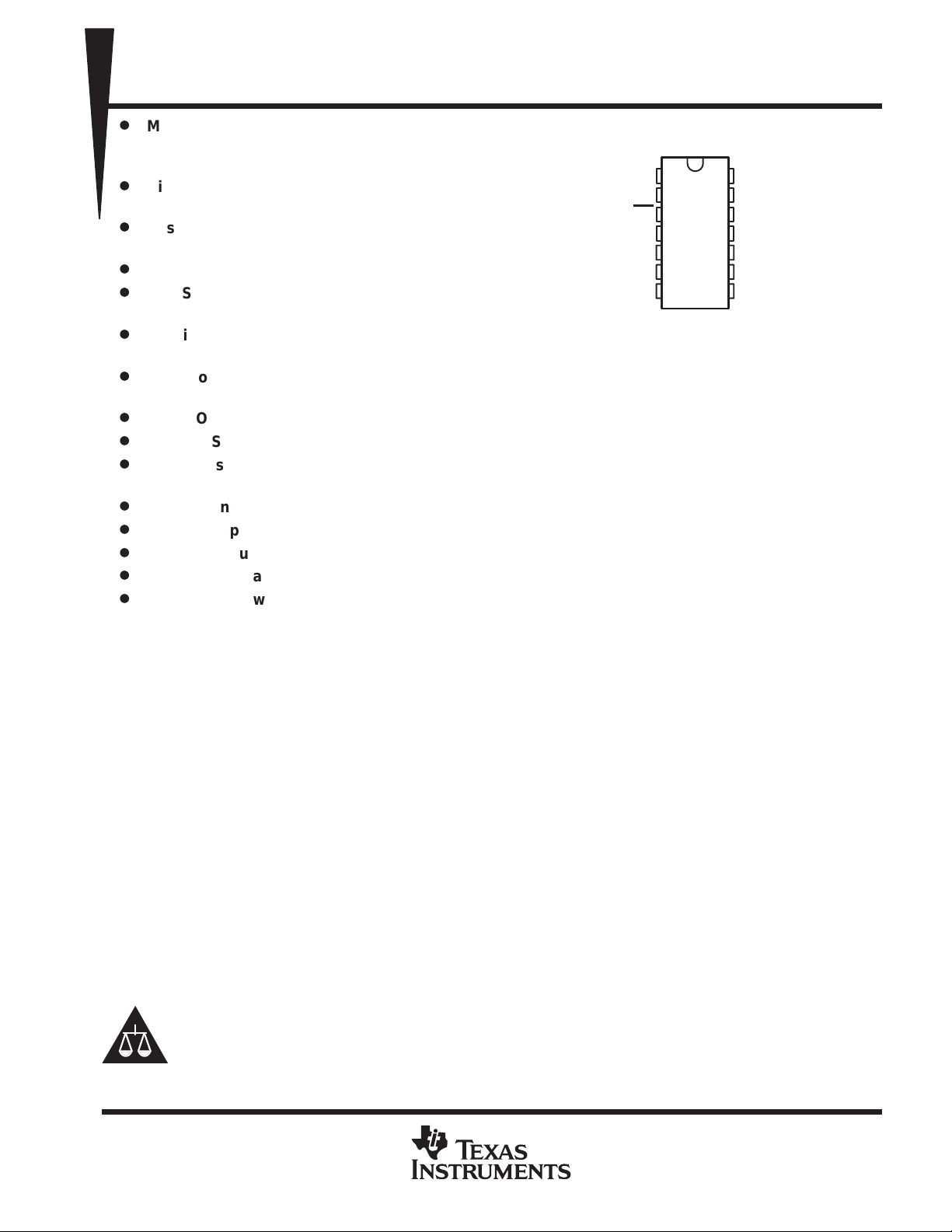
D OR N PACKAGE
(TOP VIEW)
NC
1
R
2
RE
3
DE
4
D
5
GND
6
GND
7
NC – No internal connection
14
13
12
11
10
V
CC
V
CC
A
B
Z
Y
9
8
NC
description
The SN65ALS180 and SN75ALS180 differential driver and receiver pairs are monolithic integrated
circuits designed for bidirectional data communication on multipoint bus-transmission lines. They are designed
for balanced transmission lines and meet TIA/EIA-422-B, TIA/EIA-485-A, and ITU Recommendation V.11.
The SN65ALS180 and SN75ALS180 combine a 3-state differential line driver and a differential input line
receiver, both of which operate from a single 5-V power supply. The driver and receiver have active-high and
active-low enables, respectively, that can be externally connected together to function as a direction control.
The driver differential outputs and the receiver differential inputs are connected to separate terminals for greater
flexibility and are designed to offer minimum loading to the bus when the driver is disabled or V
These ports feature wide positive and negative common-mode voltage ranges, making the device suitable for
party-line applications.
The SN65ALS180 is characterized for operation from –40°C to 85°C. The SN75ALS180 is characterized for
operation from 0°C to 70°C.
Please be aware that an important notice concerning availability, standard warranty, and use in critical applications of
Texas Instruments semiconductor products and disclaimers thereto appears at the end of this data sheet.
†
†
These devices meet or exceed the requirements of TIA/EIA-485-A, except for the Generator Contention T est (para. 3.4.2) and the Generator
These devices meet or exceed the requirements of TIA/EIA-485-A, except for the Generator Contention T est (para. 3.4.2) and the Generator
Current Limit (para. 3.4.3). The applied test voltage ranges are –6 V to 8 V for the SN75ALS180 and –4.5 V to 8 V for the SN65ALS180.
Current Limit (para. 3.4.3). The applied test voltage ranges are –6 V to 8 V for the SN75ALS180 and –4.5 V to 8 V for the SN65ALS180.
CC
= 0.
PRODUCTION DATA information is current as of publication date.
Products conform to specifications per the terms of Texas Instruments
standard warranty. Production processing does not necessarily include
testing of all parameters.
POST OFFICE BOX 655303 • DALLAS, TEXAS 75265
Copyright 1998, Texas Instruments Incorporated
1

SN65ALS180, SN75ALS180
DIFFERENTIAL DRIVER AND RECEIVER PAIRS
SLLS052E – AUGUST 1987 – REVISED OCTOBER 1998
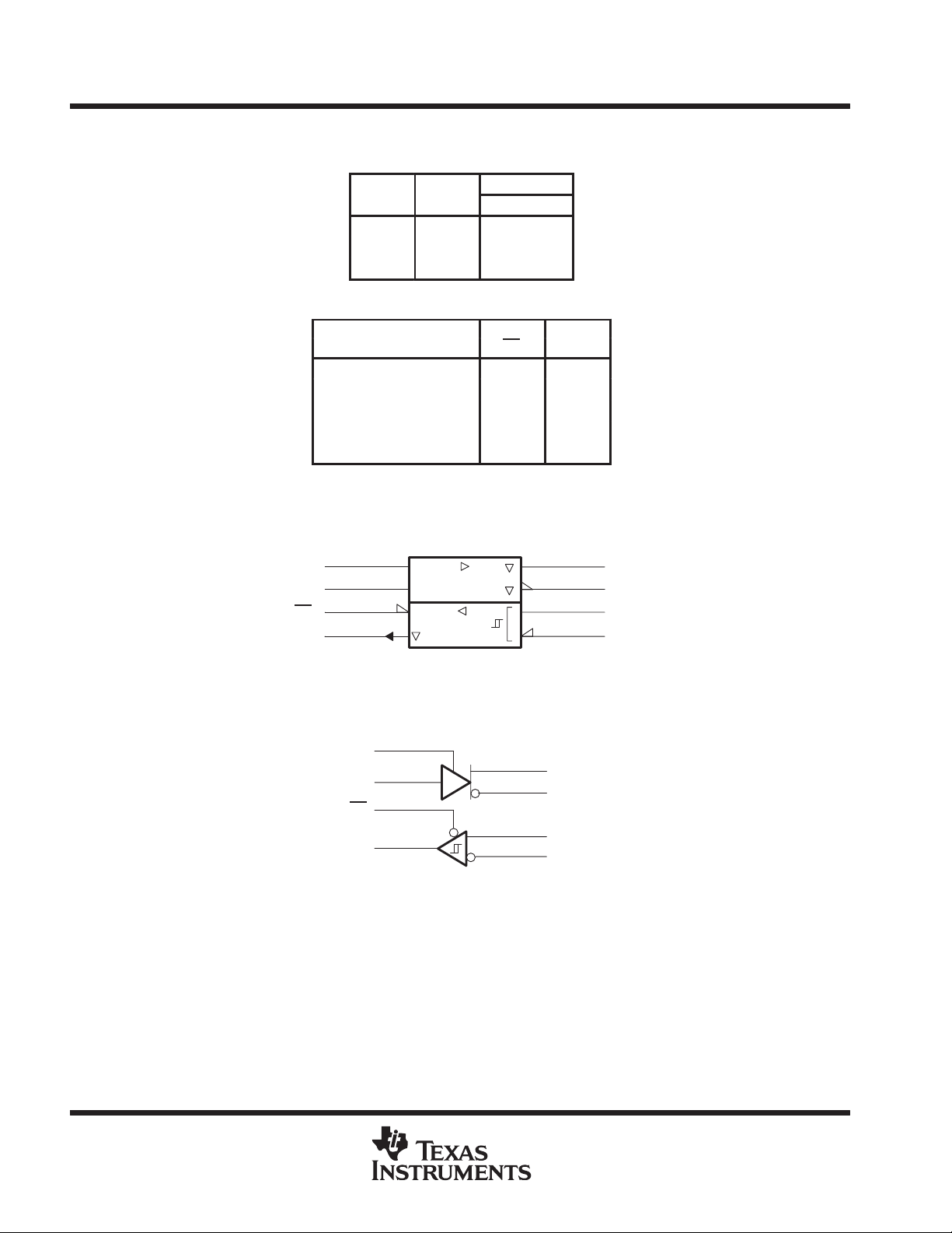
Function Tables
DRIVER
INPUT ENABLE
D DE
H H H L
L H L H
X L Z Z
RECEIVER
DIFFERENTIAL INPUTS
A–B RE R
VID ≥ 0.2 V L H
–0.2 V < VID < 0.2 V L ?
VID ≤ –0.2 V L L
X H Z
Open L H
H = high level, L = low level, ? = indeterminate,
X = irrelevant, Z = high impedance (off)
OUTPUTS
Y Z
ENABLE OUTPUT
logic symbol
†
This symbol is in accordance with ANSI/IEEE Std 91-1984 and IEC Publication 617-12.
†
DE
RE
4
5
D
3
2
R
EN1
EN2
2
1
1
logic diagram (positive logic)
4
DE
5
D
3
RE
2
R
10
10
9
Y
10
Z
12
A
11
B
9
Y
Z
9
Y
Z
2
POST OFFICE BOX 655303 • DALLAS, TEXAS 75265

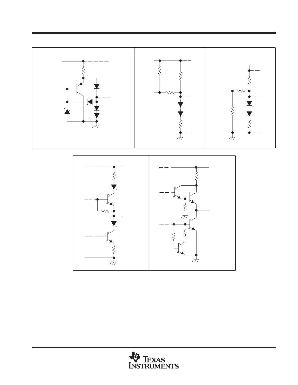
schematics of inputs and outputs
V
CC
R
(eq)
Input
SN65ALS180, SN75ALS180
DIFFERENTIAL DRIVER AND RECEIVER PAIRS
SLLS052E – AUGUST 1987 – REVISED OCTOBER 1998
RECEIVER A INPUTEQUIVALENT OF EACH INPUT RECEIVER B INPUT
18 kΩ
NOM
V
CC
3 kΩ
NOM
V
CC
Input
180 kΩ
NOM
18 kΩ
NOM
3 kΩ
NOM
Input
180 kΩ
NOM
Driver and Driver Enable Inputs: R
Receiver Enable Input: R
R
= Equivalent Resistor
(eq)
= 30 kΩ NOM
(eq)
DRIVER OUTPUT TYPICAL OF RECEIVER OUTPUT
= 12 kΩ NOM
(eq)
V
CC
Output
1.1 kΩ
NOM
85 Ω
NOM
V
CC
Output
1.1 kΩ
NOM
POST OFFICE BOX 655303 • DALLAS, TEXAS 75265
3

SN65ALS180, SN75ALS180
Voltage at any bus terminal (separately or common mode), V
or V
V
High-level output current, I
Low-level output current, I
mA
Operating free-air temperature, T
°C
DIFFERENTIAL DRIVER AND RECEIVER PAIRS
SLLS052E – AUGUST 1987 – REVISED OCTOBER 1998
absolute maximum ratings over operating free-air temperature range (unless otherwise noted)
Supply voltage, V
Voltage range at any bus terminal –10 V to 15 V. . . . . . . . . . . . . . . . . . . . . . . . . . . . . . . . . . . . . . . . . . . . . . . . . . . .
Enable input voltage, V
Package thermal impedance, θ
Storage temperature range, T
Lead temperature 1,6 mm (1/16 inch) from case for 10 seconds 260°C. . . . . . . . . . . . . . . . . . . . . . . . . . . . . . .
†
Stresses beyond those listed under “absolute maximum ratings” may cause permanent damage to the device. These are stress ratings only, and
functional operation of the device at these or any other conditions beyond those indicated under “recommended operating conditions” is not
implied. Exposure to absolute-maximum-rated conditions for extended periods may affect device reliability.
NOTES: 1. All voltage values, except differential I/O bus voltage, are with respect to network ground terminal.
2. The package thermal impedance is calculated in accordance with JESD 51, except for through-hole packages, which use a trace
length of zero.
(see Note 1) 7 V. . . . . . . . . . . . . . . . . . . . . . . . . . . . . . . . . . . . . . . . . . . . . . . . . . . . . . . . . . . . .
CC
5.5 V. . . . . . . . . . . . . . . . . . . . . . . . . . . . . . . . . . . . . . . . . . . . . . . . . . . . . . . . . . . . . . . . . . . .
I
(see Note 2): D package 127°C/W. . . . . . . . . . . . . . . . . . . . . . . . . . . . . . . . . .
JA
N package 78°C/W. . . . . . . . . . . . . . . . . . . . . . . . . . . . . . . . . . .
–65°C to 150°C. . . . . . . . . . . . . . . . . . . . . . . . . . . . . . . . . . . . . . . . . . . . . . . . . . . .
st
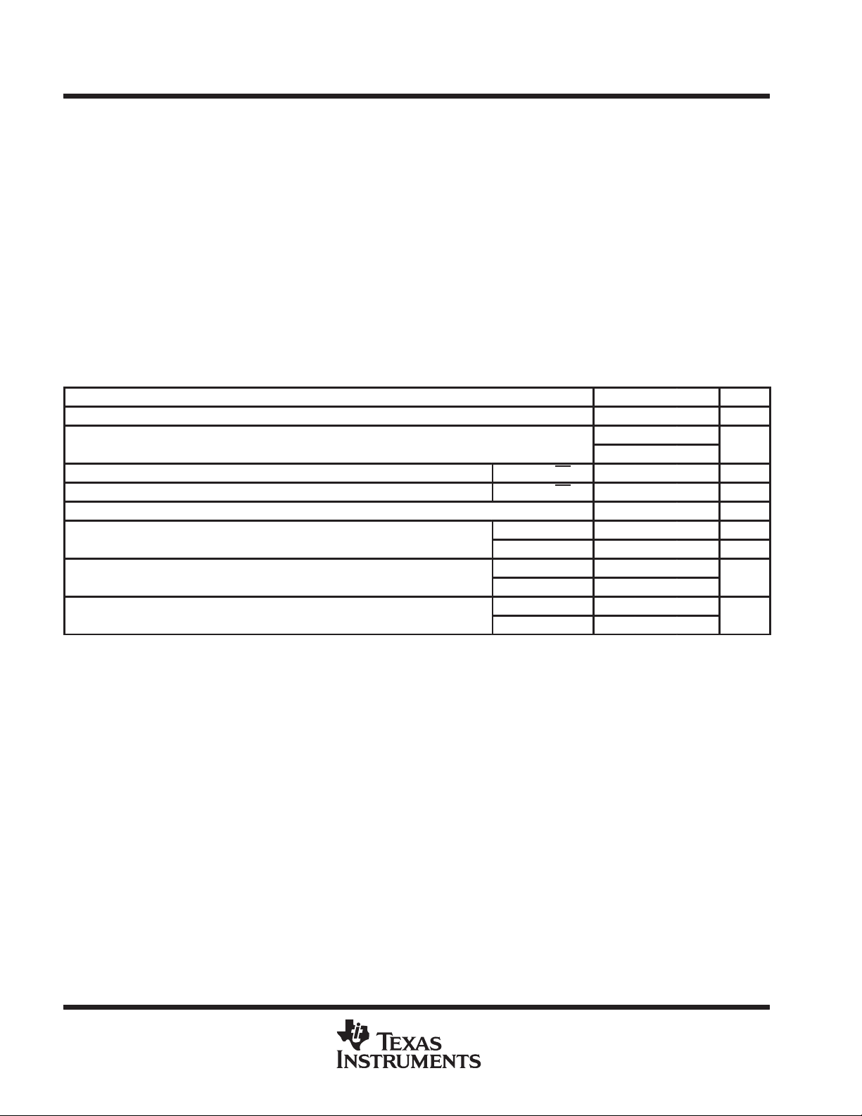
recommended operating conditions
MIN NOM MAX UNIT
Supply voltage, V
High-level input voltage, V
Low-level input voltage, V
Differential input voltage, VID (see Note 3) ±12 V
p
NOTE 3: Dif ferential-input/output bus voltage is measured at the noninverting terminal, A/Y, with respect to the inverting terminal, B/Z.
CC
p
IH
IL
p
p
OH
OL
p
A
I
IC
D, DE, and RE 2 V
D, DE, and RE 0.8 V
Driver –60 mA
Receiver –400 µA
Driver 60
Receiver 8
SN65ALS180 –40 85
SN75ALS180 0 70
4.75 5 5.25 V
12
–7
°
†
4
POST OFFICE BOX 655303 • DALLAS, TEXAS 75265
 Loading...