

查询SN54BCT25244供应商
SN54BCT25244, SN74BCT25244
25-Ω OCTAL BUFFERS/DRIVERS
WITH 3-STATE OUTPUTS
SCBS064A – JUNE 1990 – REVISED NOVEMBER 1993
• State-of-the-Art BiCMOS Design
Significantly Reduces I
CCZ
• ESD Protection Exceeds 2000 V Per
MIL-STD-883C, Method 3015; Exceeds
200 V Using Machine Model (C = 200 pF,
R = 0)
• Designed to Facilitate Incident-Wave
Switching for Line Impedances of 25 Ω
or Greater
• Distributed V
and GND Pins Minimize
CC
Noise Generated by the Simultaneous
Switching of Outputs
• Package Options Include Plastic
Small-Outline (DW) Packages, Ceramic
Chip Carriers (FK) and Flatpacks (W), and
Standard Plastic and Ceramic 300-mil DIPs
(JT, NT)
description
These 25-Ω octal buffers and line drivers are
designed specifically to improve both the
performance and density of 3-state memory
address drivers, clock drivers, and bus-oriented
receivers and transmitters.
These buffers are capable of sinking 188-mA IOL,
which facilitates switching 25-Ω transmission
lines on the incident wave. The distributed V
and GND pins minimize switching noise for more
reliable system operation.
When the output-enable (1OE
are low, the device transmits data from the
A inputs to the Y outputs. When 1OE
high, the outputs are in the high-impedance state.
and 2OE) inputs
and 2OE are
CC
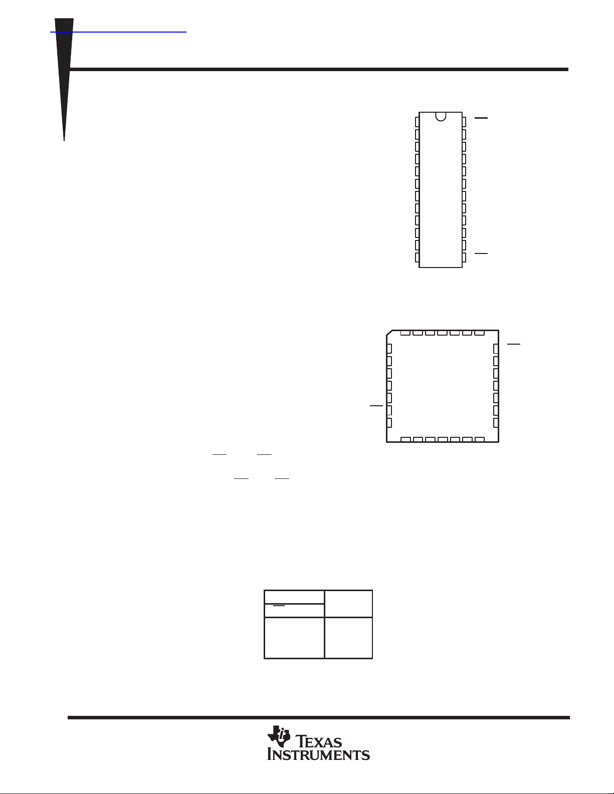
SN54BCT25244 . . . JT OR W PACKAGE
SN74BCT25244 . . . DW OR NT PACKAGE
SN54BCT25244 . . . FK PACKAGE
1A3
V
CC
1A2
NC
1A1
1OE
1Y1
NC – No internal connection
(TOP VIEW)
1
24
1Y1
GND
GND
GND
GND
2
3
1Y2
4
1Y3
5
6
1Y4
7
2Y1
8
9
2Y2
10
2Y3
11
12
2Y4
(TOP VIEW)
1A4
2A1
2A2
3212827
426
5
6
7
8
9
10
11
12 13
14 15 16 17
1Y2
1Y3
GND
1OE
23
1A1
22
1A2
21
V
CC
20
1A3
19
1A4
18
2A1
17
2A2
16
V
CC
15
2A3
14
2A4
13
2OE
CC
NCV2A3
18
NC
1Y4
GND
2A4
25
24
23
22
21
20
19
2Y1
2OE
2Y4
GND
NC
2Y3
2Y2
GND
The SN54BCT25244 is characterized for
operation over the full military temperature range
of –55°C to 125°C. The SN74BCT25244 is
characterized for operation from 0°C to 70°C.
PRODUCTION DATA information is current as of publication date.
Products conform to specifications per the terms of Texas Instruments
standard warranty. Production processing does not necessarily include
testing of all parameters.
POST OFFICE BOX 655303 • DALLAS, TEXAS 75265
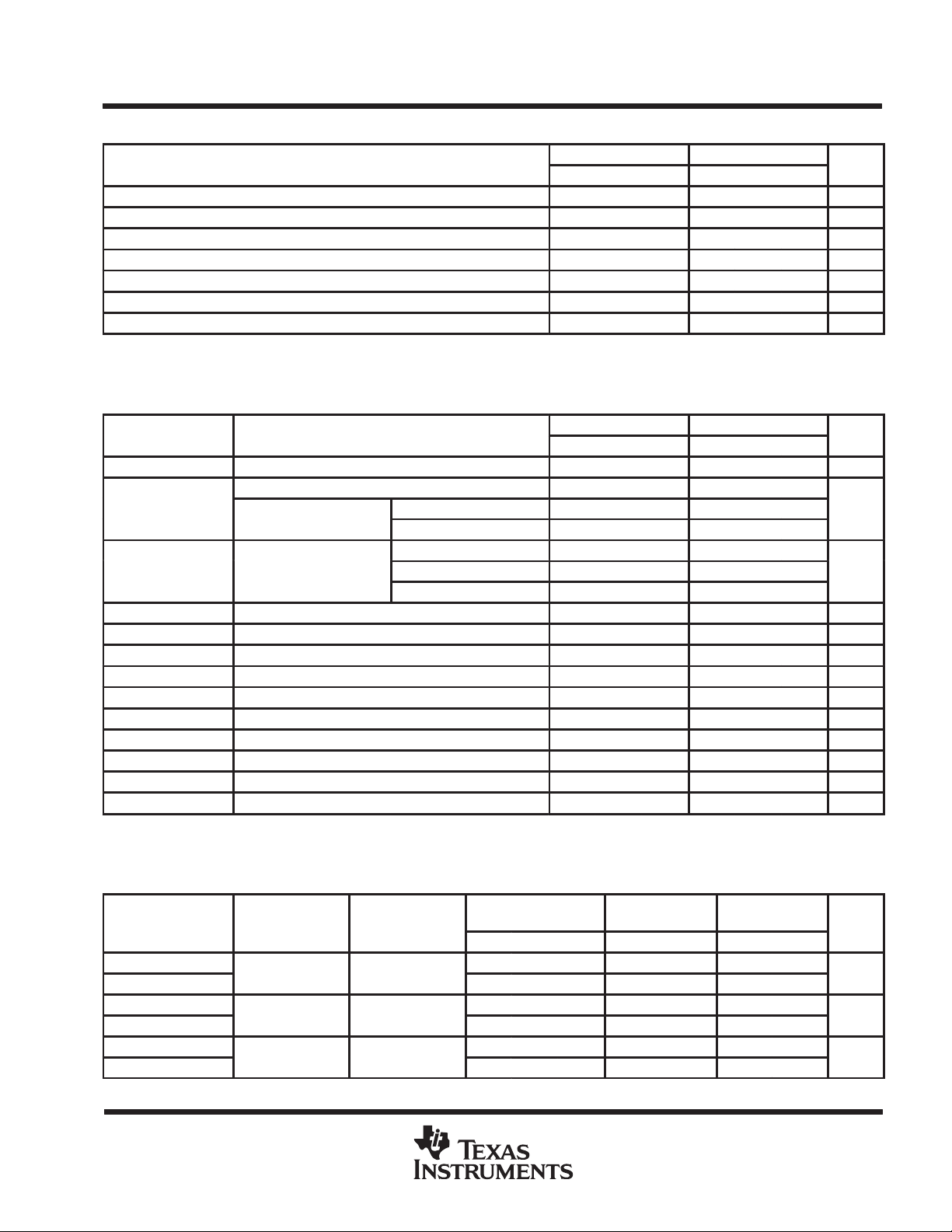
FUNCTION TABLE
(each buffer/driver)
INPUTS
OE A
L H H
L LL
H X Z
OUTPUT
Y
Copyright 1993, Texas Instruments Incorporated
2–1
SN54BCT25244, SN74BCT25244
25-Ω OCTAL BUFFERS/DRIVERS
WITH 3-STATE OUTPUTS
SCBS064A – JUNE 1990 – REVISED NOVEMBER 1993
24
23
22
20
19
13
18
17
15
14
†
EN
1
EN
1
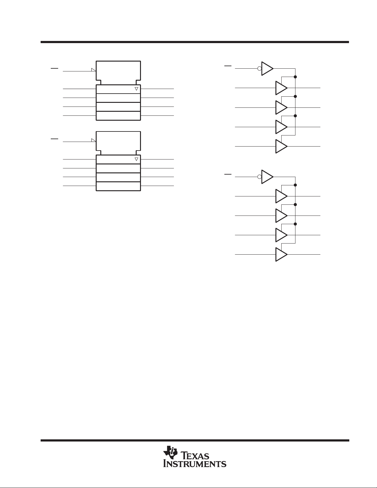
logic symbol
1OE
1A1
1A2
1A3
1A4
2OE
2A1
2A2
2A3
2A4
†
This symbol is in accordance with ANSI/IEEE Std 91-1984
and IEC Publication 617-12.
10
12
logic diagram (positive logic)
1OE
1
1Y1
3
1Y2
4
1Y3
6
1Y4
7
2Y1
9
2Y2
2Y3
2Y4
2OE
24
23 1
1A1
22 3
1A2
20 4
1A3
19 6
1A4
13
18 7
2A1
17 9
2A2 2Y2
1Y1
1Y2
1Y3
1Y4
2Y1
Pin numbers shown are for the DW, JT, NT, and W packages.
15 10
2A3
14 12
2A4
2Y3
2Y4
absolute maximum ratings over operating free-air temperature range (unless otherwise noted)
Supply voltage range, V
CC
Input voltage range, VI (see Note 1) –0.5 V to 7 V. . . . . . . . . . . . . . . . . . . . . . . . . . . . . . . . . . . . . . . . . . . . . . . . . . .
Voltage range applied to any output in the disabled or power-off state, V
Voltage range applied to any output in the high state, V
Input clamp current, I
(V
< 0) –30 mA. . . . . . . . . . . . . . . . . . . . . . . . . . . . . . . . . . . . . . . . . . . . . . . . . . . . . . . . . . . .
IK
I
. . . . . . . . . . . . . . . . . . . . . . . . . . . . . . .
O
O
Current into any output in the low state, IO: SN54BCT25244 250 mA. . . . . . . . . . . . . . . . . . . . . . . . . . . . . . . . . .
SN74BCT25244 376 mA. . . . . . . . . . . . . . . . . . . . . . . . . . . . . . . . . .
Operating free-air temperature range: SN54BCT25244 –55°C to 125°C. . . . . . . . . . . . . . . . . . . . . . . . . . . . . . .
SN74BCT25244 0°C to 70°C. . . . . . . . . . . . . . . . . . . . . . . . . . . . . . . . . . .
Storage temperature range –65°C to 150°C. . . . . . . . . . . . . . . . . . . . . . . . . . . . . . . . . . . . . . . . . . . . . . . . . . . . . . . .
‡
Stresses beyond those listed under “absolute maximum ratings” may cause permanent damage to the device. These are stress ratings only, and
functional operation of the device at these or any other conditions beyond those indicated under “recommended operating conditions” is not
implied. Exposure to absolute-maximum-rated conditions for extended periods may affect device reliability.
NOTE 1: The input and output negative-voltage ratings may be exceeded if the input and output clamp-current ratings are observed.
–0.5 V to 7 V. . . . . . . . . . . . . . . . . . . . . . . . . . . . . . . . . . . . . . . . . . . . . . . . . . . . . . . . . .
–0.5 V to 5.5 V. . . . . . . . . . . . . . . .
–0.5 V to V
‡
CC
2–2
POST OFFICE BOX 655303 • DALLAS, TEXAS 75265
SN54BCT25244, SN74BCT25244
UNIT
PARAMETER
TEST CONDITIONS
UNIT
V
4.5 V
(INPUT)
(OUTPUT)
A
Y
ns
OE
Y
ns
OE
Y
ns
25-Ω OCTAL BUFFERS/DRIVERS
WITH 3-STATE OUTPUTS
SCBS064A – JUNE 1990 – REVISED NOVEMBER 1993
recommended operating conditions (see Note 2)
SN54BCT25244 SN74BCT25244
MIN NOM MAX MIN NOM MAX
V
CC
V
IH
V
IL
I
IK
I
OH
I
OL
T
A
NOTE 2: Unused or floating inputs must be held high or low.
electrical characteristics over recommended operating free-air temperature range (unless
otherwise noted)
†
All typical values are at VCC = 5 V, TA = 25°C.
Supply voltage 4.5 5 5.5 4.5 5 5.5 V
High-level input voltage 2 2 V
Low-level input voltage 0.8 0.8 V
Input clamp current –18 –18 mA
High-level output current –53 –80 mA
Low-level output current 125 188 mA
Operating free-air temperature –55 125 0 70 °C
SN54BCT25244 SN74BCT25244
MIN TYP†MAX MIN TYP†MAX
V
IK
V
OH
V
OL
I
I
I
IH
I
IL
I
OZH
I
OZL
I
CCL
I
CCH
I
CCZ
C
i
C
o
VCC = 4.5 V, II = –18 mA –1.2 –1.2 V
VCC = 4.75 V, IOH = – 3 mA 2.7
=
CC
VCC = 4.5 V
VCC = 5.5 V, VI = 5.5 V 0.1 0.1 mA
VCC = 5.5 V, VI = 2.7 V 20 20 µA
VCC = 5.5 V, VI = 0.5 V –0.6 –0.6 mA
VCC = 5.5 V, VO = 2.7 V 50 50 µA
VCC = 5.5 V, VO = 0.5 V –50 –50 µA
VCC = 5.5 V, Outputs open 90 119 90 119 mA
VCC = 5.5 V, Outputs open 59 78 59 78 mA
VCC = 5.5 V, Outputs open 7 11 7 11 mA
VCC = 5 V, VI = 2.5 V or 0.5 V 5.5 5.5 pF
VCC = 5 V, VO = 2.5 V or 0.5 V 17 17 pF
IOH = –53 mA 2
IOH = –80 mA 2
IOL = 94 mA 0.38 0.55 0.42 0.55
IOL = 125 mA 0.8
IOL = 188 mA 0.7
V
V
switching characteristics over recommended ranges of supply voltage and operating free-air
temperature, C
PARAMETER
t
PLH
t
PHL
t
PZH
t
PZL
t
PHZ
t
PLZ
NOTE 3: Load circuits and voltage waveforms are shown in Section 1.
= 50 pF (unless otherwise noted) (see Note 3)
L
FROM
TO
POST OFFICE BOX 655303 • DALLAS, TEXAS 75265
VCC = 5 V,
TA = 25°C
MIN TYP MAX MIN MAX MIN MAX
1 3.2 4.9 1 5.6 1 5.5
2 4 5.6 2 6.3 2 6
3.2 5.6 8.5 3.2 9.7 3.2 9.3
3.7 6.3 9.2 3.7 10.4 3.7 10.2
1.6 3.6 5.5 1.6 6.5 1.6 6.3
3.1 5.3 7.8 3.1 9.5 3.1 8.4
SN54BCT25244 SN74BCT25244
UNIT
2–3

SN54BCT25244, SN74BCT25244
25-Ω OCTAL BUFFERS/DRIVERS
WITH 3-STATE OUTPUTS
SCBS064A – JUNE 1990 – REVISED NOVEMBER 1993
2–4
POST OFFICE BOX 655303 • DALLAS, TEXAS 75265

IMPORTANT NOTICE
T exas Instruments and its subsidiaries (TI) reserve the right to make changes to their products or to discontinue
any product or service without notice, and advise customers to obtain the latest version of relevant information
to verify, before placing orders, that information being relied on is current and complete. All products are sold
subject to the terms and conditions of sale supplied at the time of order acknowledgement, including those
pertaining to warranty, patent infringement, and limitation of liability.
TI warrants performance of its semiconductor products to the specifications applicable at the time of sale in
accordance with TI’s standard warranty. Testing and other quality control techniques are utilized to the extent
TI deems necessary to support this warranty . Specific testing of all parameters of each device is not necessarily
performed, except those mandated by government requirements.
CERTAIN APPLICA TIONS USING SEMICONDUCT OR PRODUCTS MAY INVOLVE POTENTIAL RISKS OF
DEATH, PERSONAL INJURY, OR SEVERE PROPERTY OR ENVIRONMENTAL DAMAGE (“CRITICAL
APPLICATIONS”). TI SEMICONDUCTOR PRODUCTS ARE NOT DESIGNED, AUTHORIZED, OR
WARRANTED TO BE SUITABLE FOR USE IN LIFE-SUPPORT DEVICES OR SYSTEMS OR OTHER
CRITICAL APPLICA TIONS. INCLUSION OF TI PRODUCTS IN SUCH APPLICATIONS IS UNDERST OOD TO
BE FULLY AT THE CUSTOMER’S RISK.
In order to minimize risks associated with the customer’s applications, adequate design and operating
safeguards must be provided by the customer to minimize inherent or procedural hazards.
TI assumes no liability for applications assistance or customer product design. TI does not warrant or represent
that any license, either express or implied, is granted under any patent right, copyright, mask work right, or other
intellectual property right of TI covering or relating to any combination, machine, or process in which such
semiconductor products or services might be or are used. TI’s publication of information regarding any third
party’s products or services does not constitute TI’s approval, warranty or endorsement thereof.
Copyright 1998, Texas Instruments Incorporated
 Loading...