

Texas Instruments SN54AS823AJT, SN74AS823ADW, SN74AS823ADWR, SN74AS823ANT, SNJ54AS823AFK Datasheet
...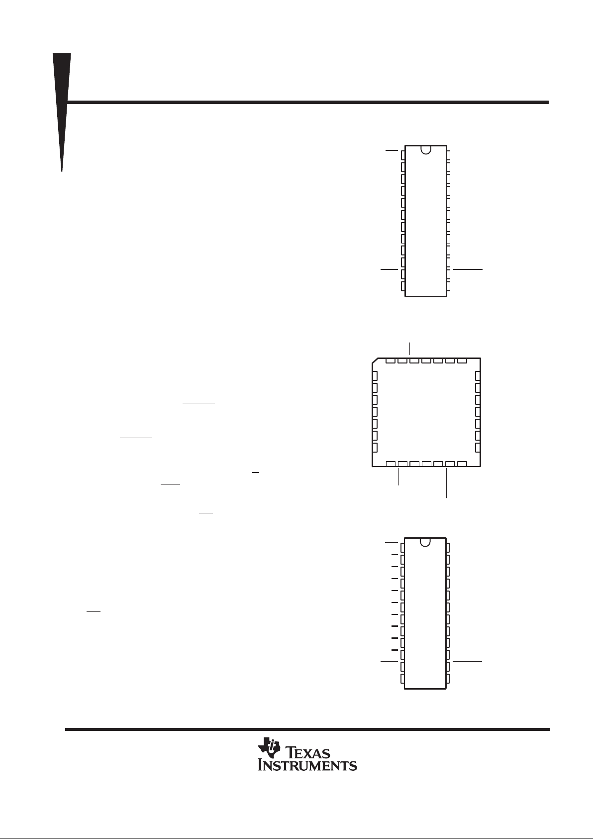
SN54AS823A . . . JT PACKAGE
SN74AS823A . . . DW OR NT PACKAGE
(TOP VIEW)
SN54AS823A . . . FK PACKAGE
(TOP VIEW)
1
2
3
4
5
6
7
8
9
10
11
12
24
23
22
21
20
19
18
17
16
15
14
13
OE
1D
2D
3D
4D
5D
6D
7D
8D
9D
CLR
GND
V
CC
1Q
2Q
3Q
4Q
5Q
6Q
7Q
8Q
9Q
CLKEN
CLK
NC – No internal connection
3212827
12 13
5
6
7
8
9
10
11
25
24
23
22
21
20
19
3Q
4Q
5Q
NC
6Q
7Q
8Q
3D
4D
5D
NC
6D
7D
8D
426
14 15 16 17 18
9D
CLR
GND
NC
CLK
CLKEN
9Q
2D1DOE
NC
1Q
2Q
V
CC
SN74AS824A . . . DW OR NT PACKAGE
(TOP VIEW)
1
2
3
4
5
6
7
8
9
10
11
12
24
23
22
21
20
19
18
17
16
15
14
13
OE
1D
2D
3D
4D
5D
6D
7D
8D
9D
CLR
GND
V
CC
1Q
2Q
3Q
4Q
5Q
6Q
7Q
8Q
9Q
CLKEN
CLK
SN54AS823A, SN74AS823A, SN74AS824A
9-BIT BUS-INTERFACE FLIP-FLOPS
WITH 3-STATE OUTPUTS
SDAS231A – JUNE 1984 – REVISED AUGUST 1995
Copyright 1995, Texas Instruments Incorporated
1
POST OFFICE BOX 655303 • DALLAS, TEXAS 75265
• Functionally Equivalent to AMD’s AM29823
and AM29824
• Provide Extra Data Width Necessary for
Wider Address/Data Paths or Buses With
Parity
• Outputs Have Undershoot-Protection
Circuitry
• Power-Up High-Impedance State
• Buffered Control Inputs to Reduce
dc Loading Effects
• Package Options Include Plastic
Small-Outline (DW) Packages, Ceramic
Chip Carriers (FK), and Standard Plastic
(NT) and Ceramic (JT) 300-mil DIPs
description
These 9-bit flip-flops feature 3-state outputs
designed specifically for driving highly capacitive
or relatively low-impedance loads. These devices
are particularly suitable for implementing wider
buffer registers, I/O ports, bidirectional bus
drivers, parity bus interfacing, and working
registers.
With the clock-enable (CLKEN
) input low, the nine
D-type edge-triggered flip-flops enter data on the
low-to-high transitions of the clock (CLK) input.
Taking CLKEN
high disables the clock buffer,
latching the outputs. The SN54AS823A and
SN74AS823A have noninverting data (D) inputs
and the SN74AS824A has inverting (D
) inputs.
Taking the clear (CLR
) input low causes the nine
Q outputs to go low independently of the clock.
A buffered output-enable (OE
) input can be used
to place the nine outputs in either a normal logic
state (high or low logic level) or the highimpedance state. In the high-impedance state, the
outputs neither load nor drive the bus lines
significantly. The high-impedance state and
increased drive provide the capability to drive bus
lines without interface or pullup components.
OE
does not affect the internal operation of the
flip-flops. Old data can be retained or new data
can be entered while the outputs are in the
high-impedance state.
The SN54AS823A is characterized for operation
over the full military temperature range of –55°C
to 125°C. The SN74AS823A and SN74AS824A
are characterized for operation from 0°C to 70°C.
PRODUCTION DATA information is current as of publication date.
Products conform to specifications per the terms of Texas Instruments
standard warranty. Production processing does not necessarily include
testing of all parameters.
SN54AS823A, SN74AS823A, SN74AS824A
9-BIT BUS-INTERFACE FLIP-FLOPS
WITH 3-STATE OUTPUTS
SDAS231A – JUNE 1984 – REVISED AUGUST 1995
2
POST OFFICE BOX 655303 • DALLAS, TEXAS 75265
Function Tables
SN54AS823A, SN74AS823A
(each flip-flop)
INPUTS
OUTPUT
OE CLR CLKEN CLK D
Q
L L X X X L
L HL↑HH
LHL↑LL
LHHXX Q
0
HXXXX Z
SN74AS824A
(each flip-flop)
INPUTS
OUTPUT
OE CLR CLKEN CLK D
Q
L L X X X L
L HL↑HL
LHL↑LH
LHHXX Q
0
HXXXX Z
logic symbols
†
EN
1
7
6D
8
7D
9
8D
10
9D
2D
2
1D
6Q
18
7Q
17
8Q
16
9Q
15
1Q
23
3
2D
4
3D
5
4D
6
5D
2Q
22
3Q
21
4Q
20
5Q
19
OE
13
CLK
1C2
R
11
CLR
G1
14
CLKEN
EN
1
7
8
9
10
2D
2
6Q
18
7Q
17
8Q
16
9Q
15
1Q
23
3
4
5
6
2Q
22
3Q
21
4Q
20
5Q
19
OE
13
CLK
1C2
R
11
CLR
G1
14
CLKEN
1D
2D
3D
4D
5D
6D
7D
8D
9D
SN54AS823A, SN74AS823A
SN74AS824A
†
These symbols are in accordance with ANSI/IEEE Std 91-1984 and IEC Publication 617-12.
Pin numbers shown are for the DW, JT, and NT packages.
SN54AS823A, SN74AS823A, SN74AS824A
9-BIT BUS-INTERFACE FLIP-FLOPS
WITH 3-STATE OUTPUTS
SDAS231A – JUNE 1984 – REVISED AUGUST 1995
3
POST OFFICE BOX 655303 • DALLAS, TEXAS 75265
logic diagrams (positive logic)
To Eight Other Channels
23
2
1
1D
1Q
R
C1
1D
CLKEN
CLK
11
14
13
OE
CLR
SN54AS823A, SN74AS823A
To Eight Other Channels
23
2
1
1D
1Q
R
C1
1D
CLKEN
CLK
11
14
13
OE
CLR
SN74AS824A
Pin numbers shown are for the DW, JT, and NT packages.
 Loading...