

Texas Instruments SN54ALS569AJ, SN74ALS568AN, SN74ALS569ADW, SN74ALS569ADWR, SN74ALS569AN Datasheet
...
SN54ALS569A, SN74ALS568A, SN74ALS569A
SYNCHRONOUS 4-BIT UP/DOWN DECADE AND BINARY COUNTERS
WITH 3-STATE OUTPUTS
SDAS229A – APRIL 1982 – REVISED JANUARY 1995
• 3-State Q Outputs Drive Bus Lines Directly
• Counter Operation Independent of 3-State
Output
• Fully Synchronous Clear, Count, and Load
• Asynchronous Clear Is Also Provided
• Fully Cascadable
• Package Options Include Plastic
Small-Outline (DW) Packages, Ceramic
Chip Carriers (FK), and Standard Plastic (N)
and Ceramic (J) 300-mil DIPs
description
The SN74ALS568A decade counter and
′ALS569A binary counters are programmable,
count up or down, and offer both synchronous and
asynchronous clearing. All synchronous functions
are executed on the positive-going edge of the
clock (CLK) input.
The clear function is initiated by applying a low
level to either asynchronous clear (ACLR
synchronous clear (SCLR
clearing overrides all other functions of the device,
while synchronous clearing overrides only the
other synchronous functions. Data is loaded from
the A, B, C, and D inputs by holding load (LOAD
low during a positive-going clock transition. The
counting function is enabled only when enable P
(ENP
) and enable T (ENT) are low and ACLR,
SCLR
, and LOAD are high. The up/down (U/D)
input controls the direction of the count. These
counters count up when U/D
down when U/D
is low.
). Asynchronous (direct)
is high and count
) or
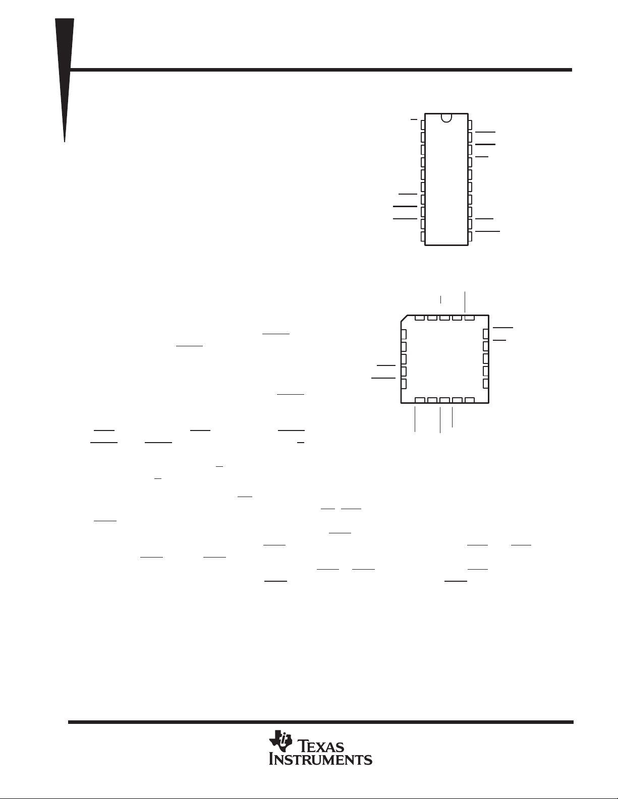
SN74ALS568A, SN74ALS569A . . . DW OR N PACKAGE
SN54ALS569A ...J PACKAGE
(TOP VIEW)
U/D
1
CLK
2
A
3
B
4
C
5
D
6
ENP
7
ACLR
SCLR
GND
SN54ALS569A . . . FK PACKAGE
B
C
D
ENP
ACLR
8
9
10
(TOP VIEW)
A
CLK
3212019
4
5
6
7
8
910111213
U/D
20
19
18
17
16
15
14
13
12
11
V
V
RCO
CCO
OE
Q
Q
Q
Q
ENT
LOAD
CC
18
17
16
15
14
CC
A
B
C
D
CCO
OE
Q
A
Q
B
Q
C
)
D
Q RCO
ENT
GND
SCLR
LOAD
A high level at the output-enable (OE
enables those outputs. Counting is independent of OE
(RCO
) to produce a low-level pulse while the count is zero (all Q outputs low) when counting down or maximum
(9 or 15) when counting up. The clocked carry output (CCO
that of the low level of the clock when RCO
otherwise, CCO
is high. CCO does not have the glitches commonly associated with a ripple-carry output.
Cascading is normally accomplished by connecting RCO
However, for very high-speed counting, RCO
) input forces the Q outputs into the high-impedance state, and a low level
. ENT is fed forward to enable the ripple-carry output
) produces a low-level pulse for a duration equal to
is low and the counter is enabled (both ENP and ENT are low);
or CCO of the first counter to ENT of the next counter.
should be used for cascading since CCO does not become active
until the clock returns to the low level.
The SN54ALS569A is characterized for operation over the full military temperature range of –55°C to 125°C.
The SN74ALS568A and SN74ALS569A are characterized for operation from 0°C to 70°C.
PRODUCTION DATA information is current as of publication date.
Products conform to specifications per the terms of Texas Instruments
standard warranty. Production processing does not necessarily include
testing of all parameters.
POST OFFICE BOX 655303 • DALLAS, TEXAS 75265
Copyright 1995, Texas Instruments Incorporated
1
SN54ALS569A, SN74ALS568A, SN74ALS569A
OPERATION
SYNCHRONOUS 4-BIT UP/DOWN DECADE AND BINARY COUNTERS
WITH 3-STATE OUTPUTS
SDAS229A – APRIL 1982 – REVISED JANUARY 1995
FUNCTION TABLE
INPUTS
OE ACLR SCLR LOAD ENT ENP U/D CLK
H X X X X X X X Q outputs disabled
L L X X X X X X Asynchronous clear
L HLXXXX↑Synchronous clear
L HHLXXX↑ Load
L HHHLLH↑ Count up
L HHHLLL↑ Count down
L H H H H X X X Inhibit count
L H H H X H X X Inhibit count
2
POST OFFICE BOX 655303 • DALLAS, TEXAS 75265
SN54ALS569A, SN74ALS568A, SN74ALS569A
SYNCHRONOUS 4-BIT UP/DOWN DECADE AND BINARY COUNTERS
WITH 3-STATE OUTPUTS
SDAS229A – APRIL 1982 – REVISED JANUARY 1995
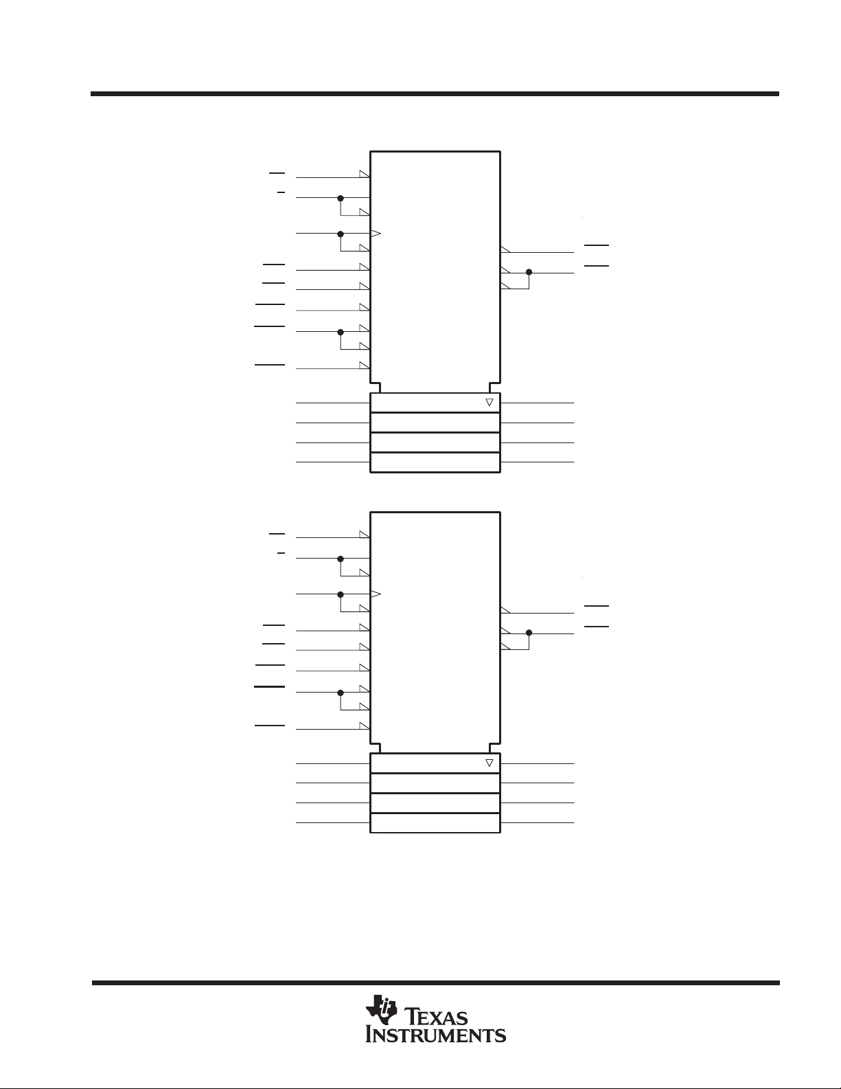
logic symbols
†
SN74ALS568A
CTRDIV10
EN10
M1 [UP]
M2 [DOWN]
C5/1,4,7,8,+/2,4,7,8–
Z6
G7
G8
5CT=0
M3 [LOAD]
M4 [COUNT]
CT=0
3,5D
1,7 (CT=9) G9
2,7 (CT=0) G9
′ALS569A
6,7,8,9
10
18
19
16
15
14
13
CCO
RCO
Q
A
Q
B
Q
C
Q
D
OE
U/D
CLK
ENT
ENP
SCLR
LOAD
ACLR
17
1
2
12
7
9
11
8
3
A
4
B
5
C
6
D
17
OE
1
U/D
2
CLK
12
ENT
7
ENP
SCLR
LOAD
ACLR
†
These symbols are in accordance with ANSI/IEEE Std 91-1984 and IEC Publication 617-12.
9
11
8
3
A
4
B
5
C
6
D
CTRDIV16
EN10
M1 [UP]
M2 [DOWN]
C5/1,4,7,8,+/2,4,7,8–
Z6
G7
G8
5CT=0
M3 [LOAD]
M4 [COUNT]
CT=0
3,5D
1,7 (CT=15) G9
2,7 (CT=0) G9
6,7,8,9
10
18
19
16
15
14
13
CCO
RCO
Q
A
Q
B
Q
C
Q
D
POST OFFICE BOX 655303 • DALLAS, TEXAS 75265
3
SN54ALS569A, SN74ALS568A, SN74ALS569A
SYNCHRONOUS 4-BIT UP/DOWN DECADE AND BINARY COUNTERS
WITH 3-STATE OUTPUTS
SDAS229A – APRIL 1982 – REVISED JANUARY 1995
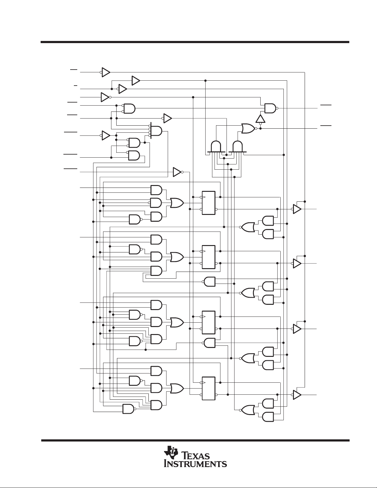
logic diagrams (positive logic)
SN74ALS568A
17
OE
1
U/D
2
CLK
12
ENT
7
ENP
SCLR
9
18
19
CCO
RCO
LOAD
ACLR
11
8
3
A
C1
1D
R
4
B
C1
1D
R
5
C
C1
1D
R
16
15
14
Q
A
Q
B
Q
C
6
D
C1
1D
R
4
POST OFFICE BOX 655303 • DALLAS, TEXAS 75265
13
Q
D
SYNCHRONOUS 4-BIT UP/DOWN DECADE AND BINARY COUNTERS
logic diagrams (positive logic) (continued)
17
OE
1
U/D
2
CLK
12
ENT
7
ENP
SCLR
9
SN54ALS569A, SN74ALS568A, SN74ALS569A
WITH 3-STATE OUTPUTS
SDAS229A – APRIL 1982 – REVISED JANUARY 1995
′ALS569A
18
CCO
19
RCO
LOAD
ACLR
11
8
3
A
C1
1D
R
4
B
C1
1D
R
5
C
C1
1D
R
16
15
14
Q
A
Q
B
Q
C
6
D
C1
1D
R
POST OFFICE BOX 655303 • DALLAS, TEXAS 75265
13
Q
D
5
SN54ALS569A, SN74ALS568A, SN74ALS569A
SYNCHRONOUS 4-BIT UP/DOWN DECADE AND BINARY COUNTERS
WITH 3-STATE OUTPUTS
SDAS229A – APRIL 1982 – REVISED JANUARY 1995
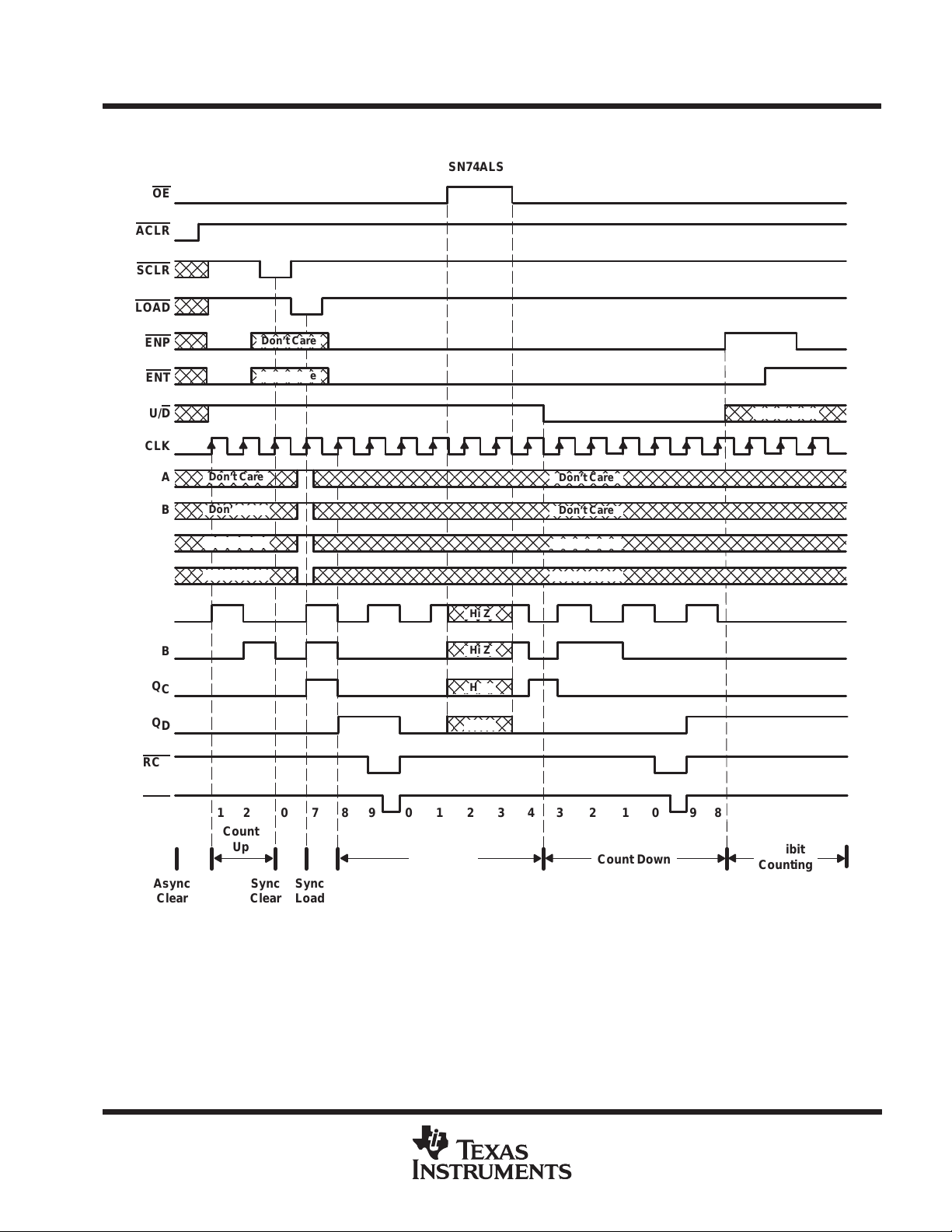
typical load, count, and inhibit sequences
SN74ALS568A
OE
ACLR
SCLR
LOAD
ENP
ENT
U/D
CLK
Q
Q
Q
Q
RCO
Don’t Care
Don’t Care
Don’t Care
A
B
C
D
A
B
C
D
Don’t Care
Don’t Care
Don’t Care
Don’t Care
Hi Z
Hi Z
Hi Z
Hi Z
Don’t Care
Don’t Care
Don’t Care
Don’t Care
CCO
Async
Clear
6
12
Count
Up
Sync
Clear
0789 0123432 10 98
Count Up
Sync
Load
POST OFFICE BOX 655303 • DALLAS, TEXAS 75265
Count Down
Inhibit
Counting

SN54ALS569A, SN74ALS568A, SN74ALS569A
SYNCHRONOUS 4-BIT UP/DOWN DECADE AND BINARY COUNTERS
typical load, count, and inhibit sequences (continued)
′ALS569A
OE
ACLR
SCLR
LOAD
SDAS229A – APRIL 1982 – REVISED JANUARY 1995
WITH 3-STATE OUTPUTS
ENP
ENT
U/D
CLK
Q
Q
Q
Q
RCO
Don’t Care
Don’t Care
Don’t Care
A
B
C
D
A
B
C
D
Don’t Care
Don’t Care
Don’t Care
Don’t Care
Hi Z
Hi Z
Hi Z
Hi Z
Don’t Care
Don’t Care
Don’t Care
Don’t Care
CCO
Async
Clear
12
Count
Up
Sync
Clear
0131415012343210 1514
Count Up
Sync
Load
POST OFFICE BOX 655303 • DALLAS, TEXAS 75265
Count Down
Inhibit
Counting
7

SN54ALS569A, SN74ALS568A, SN74ALS569A
IOHHigh-level output current
mA
IOLLow-level output current
mA
f
Clock frequenc
MH
SN74ALS568A
′ALS569A
ENP, ENT
SCLR
LOAD
SYNCHRONOUS 4-BIT UP/DOWN DECADE AND BINARY COUNTERS
WITH 3-STATE OUTPUTS
SDAS229A – APRIL 1982 – REVISED JANUARY 1995
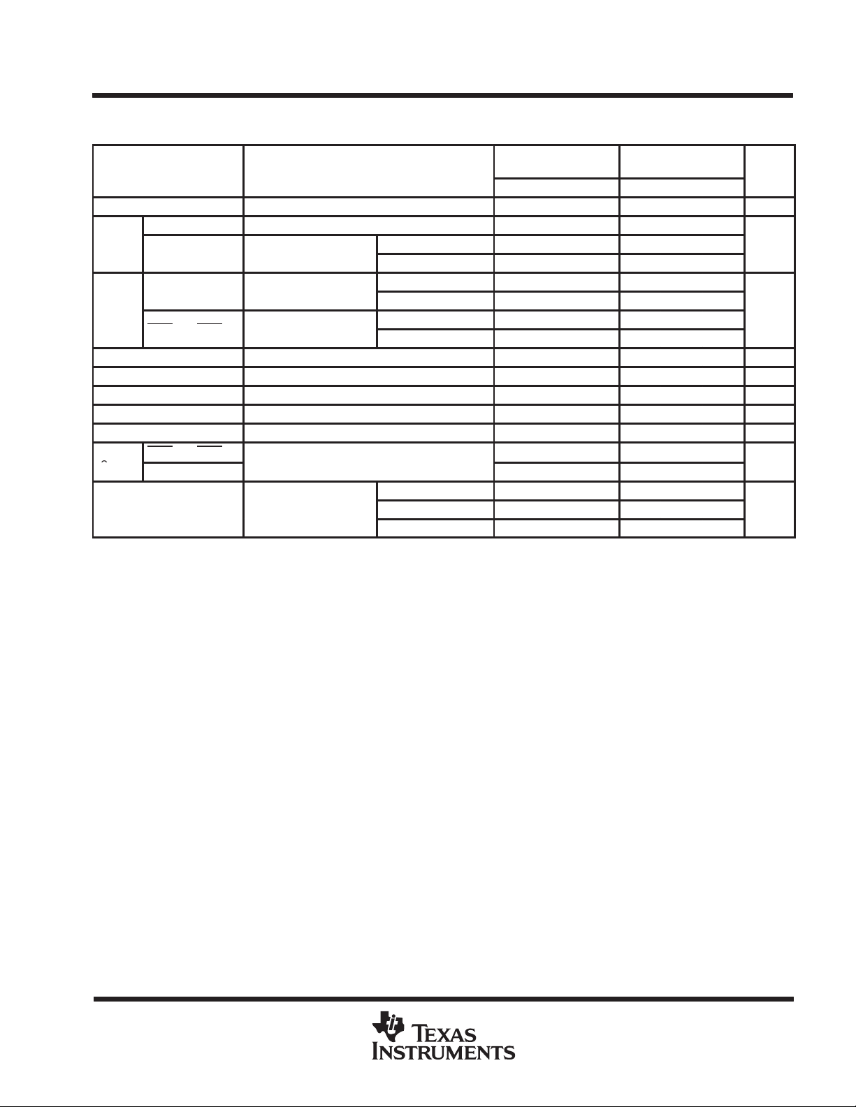
absolute maximum ratings over operating free-air temperature range (unless otherwise noted)
Supply voltage, V
Input voltage, V
Voltage applied to a disabled 3-state output 5.5 V. . . . . . . . . . . . . . . . . . . . . . . . . . . . . . . . . . . . . . . . . . . . . . . . . .
Operating free-air temperature range, T
Storage temperature range –65°C to 150°C. . . . . . . . . . . . . . . . . . . . . . . . . . . . . . . . . . . . . . . . . . . . . . . . . . . . . . .
†
Stresses beyond those listed under “absolute maximum ratings” may cause permanent damage to the device. These are stress ratings only, and
functional operation of the device at these or any other conditions beyond those indicated under “recommended operating conditions” is not
implied. Exposure to absolute-maximum-rated conditions for extended periods may affect device reliability.
7 V. . . . . . . . . . . . . . . . . . . . . . . . . . . . . . . . . . . . . . . . . . . . . . . . . . . . . . . . . . . . . . . . . . . . . . . .
CC
7 V. . . . . . . . . . . . . . . . . . . . . . . . . . . . . . . . . . . . . . . . . . . . . . . . . . . . . . . . . . . . . . . . . . . . . . . . . . . .
I
: SN54ALS569A –55°C to 125°C. . . . . . . . . . . . . . . . . . . . . . . . . . .
A
SN74ALS568A, SN74ALS569A 0°C to 70°C. . . . . . . . . . . . . . . . .
recommended operating conditions
SN74ALS568A
SN74ALS569A
UNIT
ns
ns
V
CC
V
IH
V
IL
clock
t
w
t
su
t
h
T
A
SN54ALS569A
MIN NOM MAX MIN NOM MAX
Supply voltage 4.5 5 5.5 4.5 5 5.5 V
High-level input voltage 2 2 V
Low-level input voltage 0.7 0.8 V
p
p
y
Pulse duration
Setup time before CLK↑
Hold time after CLK↑ for any input 0 0 ns
Operating free-air temperature –55 125 0 70 °C
Q outputs –1 –2.6
CCO and RCO –0.4 –0.4
Q outputs 12 24
CCO and RCO 4 8
SN74ALS568A 0 20
′ALS569A
ACLR or LOAD low 20 15
CLK high 25
CLK low 25
′
Data at A, B, C, D 25 20
U/D 35 30
ACLR inactive 10 10
CLK high 20 16.5
CLK low 23 16.5
High 35 30
Low 25 20
Low 20 15
High (inactive) 35 30
Low 20 15
High (inactive) 35 30
0 22 0 30
†
z
8
POST OFFICE BOX 655303 • DALLAS, TEXAS 75265
SN54ALS569A, SN74ALS568A, SN74ALS569A
Q outputs
V
V
Q outputs
V
4.5 V
V
V
CCO
RCO
V
V
I
‡
V
5.5 V
V
2.25 V
mA
SYNCHRONOUS 4-BIT UP/DOWN DECADE AND BINARY COUNTERS
WITH 3-STATE OUTPUTS
SDAS229A – APRIL 1982 – REVISED JANUARY 1995
electrical characteristics over recommended operating free-air temperature range (unless
otherwise noted)
PARAMETER TEST CONDITIONS
V
IK
All outputs VCC = 4.5 V to 5.5 V, IOH = –0.4 mA VCC –2 VCC –2
V
OH
OL
I
OZH
I
OZL
I
I
I
IH
I
IL
O
I
CC
†
All typical values are at VCC = 5 V, TA = 25°C.
‡
The output conditions have been chosen to produce a current that closely approximates one half of the true short-circuit output current, IOS.
p
p
and
CCO and RCO
Q outputs
VCC = 4.5 V, II = –18 mA –1.5 –1.5 V
= 4.5
CC
=
CC
= 4.5
CC
VCC = 5.5 V, VO = 2.7 V 20 20 µA
VCC = 5.5 V, VO = 0.4 V –20 –20 µA
VCC = 5.5 V, VI = 7 V 0.1 0.1 mA
VCC = 5.5 V, VI = 2.7 V 20 20 µA
VCC = 5.5 V, VI = 0.4 V –0.2 –0.2 mA
,
=
CC
VCC = 5.5 V
IOH = –1 mA 2.4 3.3
IOH = –2.6 mA 2.4 3.2
IOL = 12 mA 0.25 0.4 0.25 0.4
IOL = 24 mA 0.35 0.5
IOL = 4 mA 0.25 0.4 0.25 0.4
IOL = 8 mA 0.35 0.5
=
O
Outputs high 16 26 16 26
Outputs low 20 32 20 32
Outputs disabled 20 32 20 32
SN54ALS569A
MIN TYP†MAX MIN TYP†MAX
–15 –70 –15 –70
–20 –112 –30 –112
SN74ALS568A
SN74ALS569A
UNIT
V
mA
POST OFFICE BOX 655303 • DALLAS, TEXAS 75265
9

SN54ALS569A, SN74ALS568A, SN74ALS569A
(
)
(
)
(INPUT)
(OUTPUT)
f
MH
CLK
A
Q
ns
CLK
RCO
ns
CLK
CCO
ns
U/D
RCO
ns
ENT
RCO
ns
ENT
CCO
ns
ENP
CCO
ns
OE
A
Q
ns
OE
A
Q
ns
SYNCHRONOUS 4-BIT UP/DOWN DECADE AND BINARY COUNTERS
WITH 3-STATE OUTPUTS
SDAS229A – APRIL 1982 – REVISED JANUARY 1995
switching characteristics (see Figure 1)
VCC = 4.5 V to 5.5 V,
CL = 50 pF,
R1 = 500 Ω
PARAMETER
max
t
PLH
t
PHL
t
PLH
t
PHL
t
PLH
t
PHL
t
PLH
t
PHL
t
PLH
t
PHL
t
PLH
t
PHL
t
PLH
t
PHL
t
PHL
t
PZH
t
PZL
t
PHZ
t
†
For conditions shown as MIN or MAX, use the appropriate value specified under recommended operating conditions.
PLZ
FROM
INPUT
SN74ALS568A 20
′ALS569A 22 30
ACLR Any Q
TO
OUTPUT
ny
ny
ny
R2 = 500 Ω,
TA = MIN to MAX
SN54ALS569A
MIN MAX MIN MAX
4 21 4 13
7 19 7 16
12 37 12 28
10 28 10 19
5 17 5 13
6 30 6 25
9 31 9 23
9 33 9 19
6 21 6 15
4 20 4 13
5 18 5 13
9 32 9 23
4 18 4 12
5 18 5 14
9 25 9 20 ns
6 23 6 18
6 29 6 24
1 12 1 10
3 29 3 13
,
†
SN74ALS568A
SN74ALS569A
UNIT
z
10
POST OFFICE BOX 655303 • DALLAS, TEXAS 75265
From Output
Under Test
(see Note A)
SN54ALS569A, SN74ALS568A, SN74ALS569A
SYNCHRONOUS 4-BIT UP/DOWN DECADE AND BINARY COUNTERS
WITH 3-STATE OUTPUTS
SDAS229A – APRIL 1982 – REVISED JANUARY 1995
PARAMETER MEASUREMENT INFORMATION
SERIES 54ALS/74ALS AND 54AS/74AS DEVICES
7 V
V
CC
S1
R
L
Test
Point
C
L
R
L
From Output
Under Test
C
(see Note A)
Test
Point
L
From Output
Under Test
(see Note A)
R1
C
L
RL = R1 = R2
Test
Point
R2
LOAD CIRCUIT FOR
BI-STATE
TOTEM-POLE OUTPUTS
Timing
Input
t
su
Data
Input
VOLTAGE WAVEFORMS
SETUP AND HOLD TIMES
Output
Control
(low-level
enabling)
Waveform 1
S1 Closed
(see Note B)
Waveform 2
S1 Open
(see Note B)
t
PZL
t
PZH
ENABLE AND DISABLE TIMES, 3-STATE OUTPUTS
VOLTAGE WAVEFORMS
1.3 V
t
PHZ
1.3 V
1.3 V
t
1.3 V1.3 V
1.3 V1.3 V
FOR OPEN-COLLECTOR OUTPUTS
h
t
PLZ
LOAD CIRCUIT
3.5 V
0.3 V
3.5 V
0.3 V
3.5 V
0.3 V
[
3.5 V
V
OL
0.3 V
V
OH
0.3 V
[
0 V
High-Level
Low-Level
Out-of-Phase
(see Note C)
Pulse
Pulse
Input
In-Phase
Output
Output
LOAD CIRCUIT
FOR 3-STATE OUTPUTS
1.3 V 1.3 V
t
w
1.3 V 1.3 V
VOLTAGE WAVEFORMS
PULSE DURATIONS
1.3 V 1.3 V
t
PLH
t
PHL
1.3 V 1.3 V
VOLTAGE WAVEFORMS
PROPAGATION DELAY TIMES
1.3 V1.3 V
t
PHL
t
PLH
3.5 V
0.3 V
3.5 V
0.3 V
3.5 V
0.3 V
V
V
V
V
OH
OL
OH
OL
NOTES: A. CL includes probe and jig capacitance.
B. Waveform 1 is for an output with internal conditions such that the output is low except when disabled by the output control.
Waveform 2 is for an output with internal conditions such that the output is high except when disabled by the output control.
C. When measuring propagation delay items of 3-state outputs, switch S1 is open.
D. All input pulses have the following characteristics: PRR ≤ 1 MHz, tr = tf = 2 ns, duty cycle = 50%.
E. The outputs are measured one at a time with one transition per measurement.
Figure 1. Load Circuits and Voltage Waveforms
POST OFFICE BOX 655303 • DALLAS, TEXAS 75265
11

IMPORTANT NOTICE
T exas Instruments and its subsidiaries (TI) reserve the right to make changes to their products or to discontinue
any product or service without notice, and advise customers to obtain the latest version of relevant information
to verify, before placing orders, that information being relied on is current and complete. All products are sold
subject to the terms and conditions of sale supplied at the time of order acknowledgement, including those
pertaining to warranty, patent infringement, and limitation of liability.
TI warrants performance of its semiconductor products to the specifications applicable at the time of sale in
accordance with TI’s standard warranty. Testing and other quality control techniques are utilized to the extent
TI deems necessary to support this warranty . Specific testing of all parameters of each device is not necessarily
performed, except those mandated by government requirements.
CERT AIN APPLICATIONS USING SEMICONDUCTOR PRODUCTS MAY INVOLVE POTENTIAL RISKS OF
DEATH, PERSONAL INJURY, OR SEVERE PROPERTY OR ENVIRONMENTAL DAMAGE (“CRITICAL
APPLICATIONS”). TI SEMICONDUCTOR PRODUCTS ARE NOT DESIGNED, AUTHORIZED, OR
WARRANTED TO BE SUITABLE FOR USE IN LIFE-SUPPORT DEVICES OR SYSTEMS OR OTHER
CRITICAL APPLICA TIONS. INCLUSION OF TI PRODUCTS IN SUCH APPLICATIONS IS UNDERST OOD TO
BE FULLY AT THE CUSTOMER’S RISK.
In order to minimize risks associated with the customer’s applications, adequate design and operating
safeguards must be provided by the customer to minimize inherent or procedural hazards.
TI assumes no liability for applications assistance or customer product design. TI does not warrant or represent
that any license, either express or implied, is granted under any patent right, copyright, mask work right, or other
intellectual property right of TI covering or relating to any combination, machine, or process in which such
semiconductor products or services might be or are used. TI’s publication of information regarding any third
party’s products or services does not constitute TI’s approval, warranty or endorsement thereof.
Copyright 1998, Texas Instruments Incorporated
 Loading...