

Page 1
SN100KT5539
OCTAL ECL-TO-TTL TRANSLATOR
WITH OPEN-COLLECTOR OUTPUTS
SDZS008 – JANUARY 1990 – REVISED OCTOBER 1990
• 100K Compatible
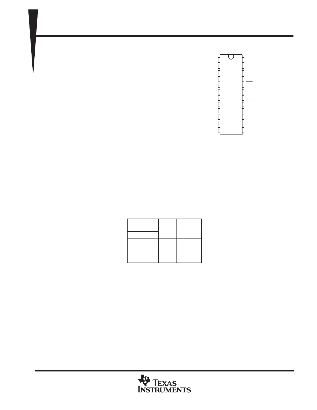
R NT PACKAGE
(T0P VIEW)
• Open-Collector Outputs Drive Bus Lines or
Y1
Buffer Memory Address Registers
• ECL and TTL Output-Enable Inputs
• Flow-Through Architecture Optimizes PCB
Layout
• Center-Pin V
, VEE, and GND
CC
Configurations Minimize High-Speed
Switching Noise
• Package Options Include “Small Outline”
Packages and Standard Plastic 300-mil
DIPs
GND
GND
GND
1
Y2
2
Y3
3
Y4
4
V
5
CC
6
7
8
Y5
9
Y6
10
Y7
11
Y8
12
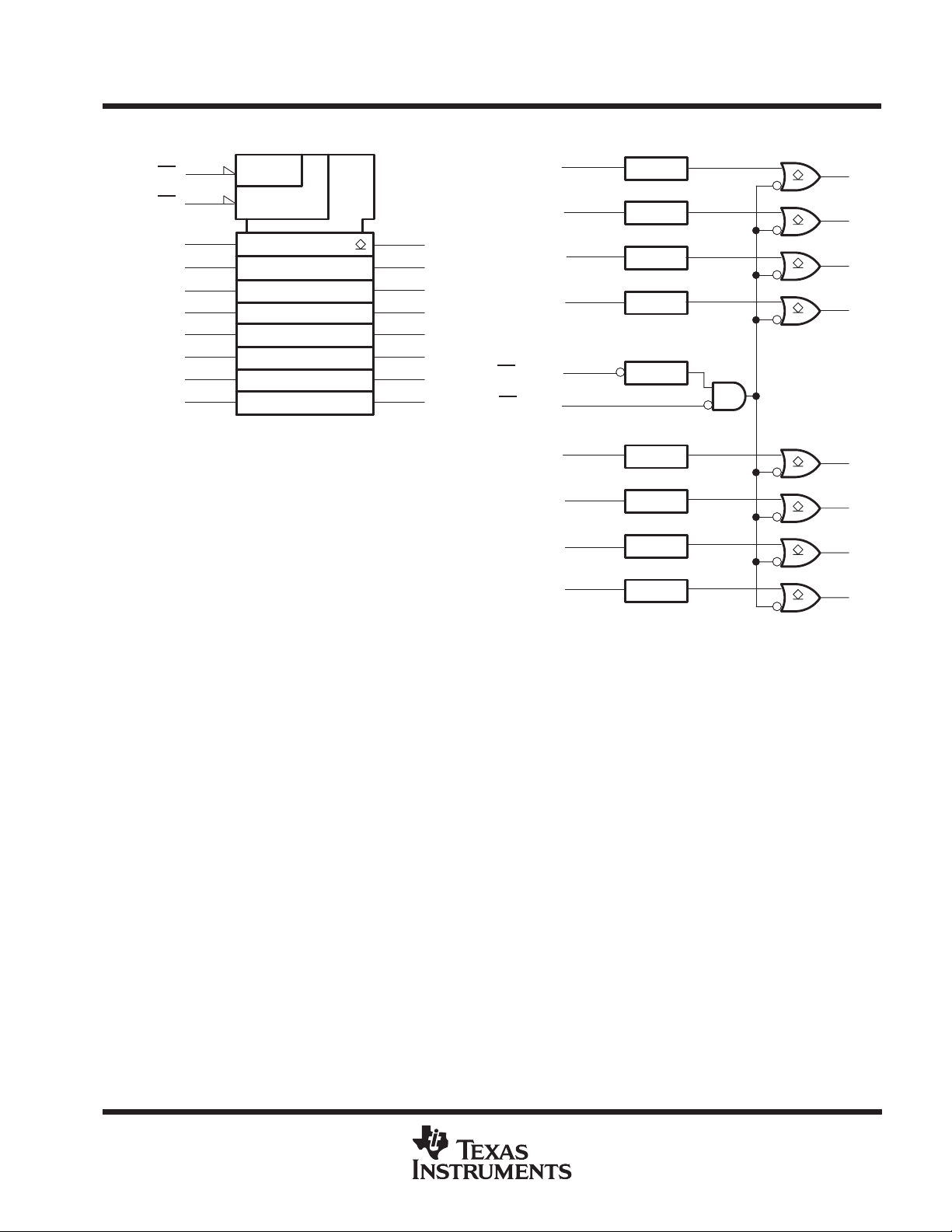
description
This octal ECL-to-TTL translator is designed to provide efficient translation between a 100K signal environment
and a TTL signal environment. This device is designed specifically to improve the performance and density of
ECL-to-TTL CPU/bus-oriented functions such as memory-address drivers, clock drivers, and bus-oriented
receivers and transmitters while eliminating the need for three-state overlap protection.
Two pins OE
1 being ECL-compatible and OE2 being TTL-compatible. This offers the choice of controlling the outputs
OE
of the device from either a TTL or ECL signal environment.
1 and OE2 are provided for output-enable control. These control inputs are ANDed together with
24
23
22
21
20
19
18
17
16
15
14
13
A1
A2
A3
A4
OE
V
EE
GND
OE
A5
A6
A7
A8
2 (TTL)
1 (ECL)
The SN100KT5539 is characterized for operation from 0°C to 85°C.
FUNCTION TABLE
OUTPUT
ENABLE INPUT (TTL)
OE1 OE2 A Y
H X X H
X HX H
LLL L
LLH H
DATA OUTPUT
PRODUCTION DATA information is current as of publication date.
Products conform to specifications per the terms of Texas Instruments
standard warranty. Production processing does not necessarily include
testing of all parameters.
POST OFFICE BOX 655303 • DALLAS, TEXAS 75265
Copyright 1990, Texas Instruments Incorporated
1
Page 2
SN100KT5539
OCTAL ECL-TO-TTL TRANSLATOR
WITH OPEN-COLLECTOR OUTPUTS
SDZS008 – JANUARY 1990 – REVISED OCTOBER 1990
A2
A3
A4
A5
A6
A7
A8
†
17
20
2
24
23
22
21
16
15
14
13
ECL/TTL
&
EN
ECL/TTL
logic symbol
OE1
OE
†
This symbol is in accordance with ANSI/IEEE Std 91-1984
and IEC Publication 617-12.
10
11
12
logic diagram (positive logic)
24
A1
23
A2
1
Y1A1
2
Y2
3
Y3
4
Y4
9
Y5
Y6
Y7
Y8
OE1 (ECL)
2 (TTL)
OE
A3
A4
A5
A6
A7
22
21
17
20
16
15
14
ECL/TTL
ECL/TTL
ECL/TTL
ECL/TTL
ECL/TTL
ECL/TTL
ECL/TTL
ECL/TTL
10
11
1
Y1
2
Y2
3
Y3
4
Y4
9
Y5
Y6
Y7
A8
13
ECL/TTL
12
absolute maximum ratings over operating free-air temperature range (unless otherwise noted)
Supply voltage range, V
Supply voltage range, V
Input voltage range: TTL (see Note 1) –1.2 V to 7 V. . . . . . . . . . . . . . . . . . . . . . . . . . . . . . . . . . . . . . . . . . . . . . . .
Input current range: TTL –30 mA to 5 mA. . . . . . . . . . . . . . . . . . . . . . . . . . . . . . . . . . . . . . . . . . . . . . . . . . . . . . . . .
Voltage applied to any output in the high state –0.5 V to V
Current into any output in the low state 96 mA. . . . . . . . . . . . . . . . . . . . . . . . . . . . . . . . . . . . . . . . . . . . . . . . . . . . .
Operating free-air temperature range 0°C to 85°C. . . . . . . . . . . . . . . . . . . . . . . . . . . . . . . . . . . . . . . . . . . . . . . . . .
Storage temperature range –65°C to 150°C. . . . . . . . . . . . . . . . . . . . . . . . . . . . . . . . . . . . . . . . . . . . . . . . . . . . . . .
‡
Stresses beyond those listed under “absolute maximum ratings” may cause permanent damage to the device. These are stress ratings only and
functional operation of the device at these or any other conditions beyond those indicated under “recommended operating conditions” is not
implied. Exposure to absolute-maximum-rated conditions for extended periods may affect device reliability.
NOTE 1: The TTL input voltage ratings may be exceeded provided the input current ratings are observed.
–0.5 V to 7 V. . . . . . . . . . . . . . . . . . . . . . . . . . . . . . . . . . . . . . . . . . . . . . . . . . . . . . . . . .
CC
–8 V to 0 V. . . . . . . . . . . . . . . . . . . . . . . . . . . . . . . . . . . . . . . . . . . . . . . . . . . . . . . . . . .
EE
ECL V
. . . . . . . . . . . . . . . . . . . . . . . . . . . . . . . . . . . . . . . .
EE
to 0 V. . . . . . . . . . . . . . . . . . . . . . . . . . . . . . . . . . . . . . . . . . . . . . . . . . . . . . . . . . . . .
Y8
‡
CC
2
POST OFFICE BOX 655303 • DALLAS, TEXAS 75265
Page 3

SN100KT5539
OCTAL ECL-TO-TTL TRANSLATOR
WITH OPEN-COLLECTOR OUTPUTS
SDZS008 – JANUARY 1990 – REVISED OCTOBER 1990
recommended operating conditions
MIN NOM MAX UNIT
V
CC
V
EE
V
IH
V
IL
V
IH
V
IL
V
OH
I
OL
I
IK
T
A
†
The algebraic convention, in which the least positive (most negative) value is designated minimum, is used in this data sheet for logic levels only.
electrical characteristics over recommended operating free-air temperature range (unless
otherwise noted)
V
IK
I
OH
V
OL
I
I
I
IH
I
IL
I
CCH
I
CCL
I
EE
C
i
C
o
‡
All typical values are at VCC = 5 V, VEE = –4.5 V, TA = 25°C.
TTL supply voltage 4.5 5 5.5 V
ECL supply voltage –4.2 –4.5 –4.8 V
TTL high-level input voltage 2 V
TTL low-level input voltage 0.8 V
ECL high-level input voltage
ECL low-level input voltage
TTL high-level output voltage 5.5 V
TTL low-level output current 48 mA
TTL input clamp current –18 mA
Operating free-air temperature range 0 85 °C
PARAMETER TEST CONDITIONS MIN TYP‡MAX UNIT
OE2 only VCC = 4.5 V, VEE = –4.2 V, II = –18 mA –1.2 V
OE2 only VCC = 5.5 V, VEE = –4.8 V, VI = 7 V 0.1 mA
OE2 only VCC = 5.5 V, VEE = –4.8 V, VI = 2.7 V 20 µA
A inputs and OE1 VCC = 5.5 V, VEE = –4.8 V, VI = –840 mV 350 µA
OE2 only VCC = 5.5 V, VEE = –4.8 V, VI = 0.5 V –0.5 mA
A inputs and OE1 VCC = 5.5 V, VEE = –4.8 V, VI = –1810 mV 0.5 µA
†
†
VCC = 4.5 V, VEE = –4.2 V, VOH = 5.5 V 250 µA
VCC = 4.5 V, VEE = –4.5 V ± 0.3 V, IOL = 48 mA 0.38 0.55 V
VCC = 5.5 V, VEE = –4.8 V 63 91 mA
VCC = 5.5 V, VEE = –4.8 V 79 114 mA
VCC = 5.5 V, VEE = –4.2 V –22 –32 mA
VCC = 5 V, VEE = –4.5 V 6 pF
VCC = 5 V, VEE = –4.5 V 5 pF
–1150 –840 mV
–1810 –1490 mV
POST OFFICE BOX 655303 • DALLAS, TEXAS 75265
3
Page 4

SN100KT5539
OCTAL ECL-TO-TTL TRANSLATOR
WITH OPEN-COLLECTOR OUTPUTS
SDZS008 – JANUARY 1990 – REVISED OCTOBER 1990
switching characteristics over recommended ranges of supply voltage and operating free-air
temperature (unless otherwise noted) (see Figure 1)
CL = 50 pF,
FROM TO R1 = 500 Ω,
(INPUT) (OUTPUT) R2 = 500 Ω
t
PLH
t
PHL
t
PLH
t
PHL
t
PLH
t
PHL
All typical values are at VCC = 5 V, VEE = –4.5 V, TA = 25°C.
OE
OE
Any A
1 (ECL)
2 (TTL)
MIN TYP†MAX
Y
Y
Y
6.2 9.3 12.4
2.6 4.9 7.3
7.1 10.3 13.5
3.2 5.8 8.4
6.5 9.5 12.4
2.7 5.3 8
UNITPARAMETER
ns
ns
ns
4
POST OFFICE BOX 655303 • DALLAS, TEXAS 75265
Page 5

OCTAL ECL-TO-TTL TRANSLATOR
WITH OPEN-COLLECTOR OUTPUTS
SDZS008 – JANUARY 1990 – REVISED OCTOBER 1990
PARAMETER MEASUREMENT INFORMATION
7 V
R1
SN100KT5539
From Output
Under Test
(See Note A)
Input
(See Note B)
t
PLH
In-Phase
Output
t
PHL
Out-of-Phase
Output
TTL-INPUT PROPAGATION DELAY TIMES
NOTES: A.CL includes probe and jig capacitance.
B.For TTL inputs, input pulses are supplied by generators having the following characteristics: PRR ≤ 10 MHz, Zo = 50 Ω, tr ≤ 2.5 ns,
tf ≤ 2.5 ns.
C.For ECL inputs, input pulses are supplied by generators having the following characteristics: PRR ≤ 10 MHz, Zo = 50 Ω, tr ≤ 0.7 ns,
tf ≤ 0.7 ns.
D.The outputs are measured one at a time with one transition per measurement.
1.5 V 1.5 V
1.5 V
1.5 V 1.5 V
C
L
LOAD CIRCUIT
3 V
0
t
PHL
V
1.5 V
V
t
PLH
V
V
OH
OL
OH
OL
R2
Input
(See Note C)
In-Phase
Output
Out-of-Phase
Output
Test Point
t
r
80% 80%
20%
t
PLH
t
PHL
ECL-INPUT PROPAGATION DELAY TIMES
50%
50%
1.5 V
1.5 V 1.5 V
20%
t
f
t
PHL
1.5 V
t
PLH
–950 mV
–1690 mV
V
OH
V
OL
V
OH
V
OL
FIGURE 1. LOAD CIRCUIT AND VOLTAGE WA VEFORMS
POST OFFICE BOX 655303 • DALLAS, TEXAS 75265
5
Page 6

IMPORTANT NOTICE
T exas Instruments and its subsidiaries (TI) reserve the right to make changes to their products or to discontinue
any product or service without notice, and advise customers to obtain the latest version of relevant information
to verify, before placing orders, that information being relied on is current and complete. All products are sold
subject to the terms and conditions of sale supplied at the time of order acknowledgement, including those
pertaining to warranty, patent infringement, and limitation of liability.
TI warrants performance of its semiconductor products to the specifications applicable at the time of sale in
accordance with TI’s standard warranty. Testing and other quality control techniques are utilized to the extent
TI deems necessary to support this warranty . Specific testing of all parameters of each device is not necessarily
performed, except those mandated by government requirements.
CERT AIN APPLICATIONS USING SEMICONDUCTOR PRODUCTS MAY INVOLVE POTENTIAL RISKS OF
DEATH, PERSONAL INJURY, OR SEVERE PROPERTY OR ENVIRONMENTAL DAMAGE (“CRITICAL
APPLICATIONS”). TI SEMICONDUCTOR PRODUCTS ARE NOT DESIGNED, AUTHORIZED, OR
WARRANTED TO BE SUITABLE FOR USE IN LIFE-SUPPORT DEVICES OR SYSTEMS OR OTHER
CRITICAL APPLICA TIONS. INCLUSION OF TI PRODUCTS IN SUCH APPLICATIONS IS UNDERST OOD TO
BE FULLY AT THE CUSTOMER’S RISK.
In order to minimize risks associated with the customer’s applications, adequate design and operating
safeguards must be provided by the customer to minimize inherent or procedural hazards.
TI assumes no liability for applications assistance or customer product design. TI does not warrant or represent
that any license, either express or implied, is granted under any patent right, copyright, mask work right, or other
intellectual property right of TI covering or relating to any combination, machine, or process in which such
semiconductor products or services might be or are used. TI’s publication of information regarding any third
party’s products or services does not constitute TI’s approval, warranty or endorsement thereof.
Copyright 1998, Texas Instruments Incorporated
 Loading...