

查询PTB48560C供应商
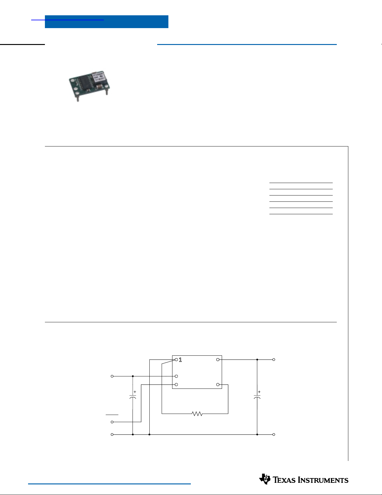
PTH05000W —5-V Input
6-A, 5-V Input Non-Isolated
Wide-Output Adjust Power Module
NOMINAL SIZE = 0.75 in x 0.5 in
(19,05 mm x 12,7 mm)
Description
The PTH05000 series of non-isolated
power modules are small in size and high
on performance. Using double-sided surface mount construction and synchronous
rectification technology, these regulators
deliver up to 6 A of output current while
occupying a PCB area of about half the
size of a standard postage stamp. They
are an ideal choice for applications where
space, performance and cost are important design constraints.
The series operates from an input
voltage of 5 V to provide step-down
power conversion to any output voltage
over the range, 0.9 V to 3.6 V. The output voltage of the PTH05000W is set
within this range using a single resistor.
SLTS201C – MAY 2003 – REVISED DECEMBER 2003
Features
• Up to 6-A Output Current
• 5-V Input Voltage
• Wide-Output Voltage Adjust
(0.9 V to 3.6 V)
• Efficiencies up to 94 %
• 160 W/in³ Power Density
• On/Off Inhibit
• Under-Voltage Lockout
Operating features include an on/off
inhibit, output voltage adjust (trim), an
output current limit, and over-temperature protection.
For high efficiency these parts employ
a synchronous rectifier output stage. An
output pre-bias holdoff capability ensures
that the output will not sink current during startup.
Target applications include telecom,
industrial, and general purpose circuits,
including low-power dual-voltage systems
that use a DSP, microprocessor, or ASIC.
Package options include both throughhole and surface mount configurations.
• Output Current Limit
• Pre-Bias Startup Capability
• Over-Temperature Protection
• Surface Mountable
• Operating Temp: –40 to +85 °C
• Safety Agency Approvals (Pending):
UL 1950, CSA 22.2 950, EN60950
& VDE
Pin Configuration
Pin Function
1 GND
2V
in
3 Inhibit *
4Vo Adjust
5V
out
* Denotes negative logic:
Open = Output On
Ground = Output Off
Standard Application
R
= Required to set the output voltage to a value
set
higher than 0.9 V. See spec. table for values.
Cin= Required 330 µF capacitor
C
= Optional 100 µF capacitor
out
V
IN
C
IN
330 µF
(Required)
Inhibit
GND
For technical support and further information visit http://power.ti.com
1
2
3
PTH05000W
(Top View)
R
SET
1 %, 0.1 W
(Required)
5
4
C
OUT
100 µF
Electrolytic
(Optional)
V
OUT
GND

PTH05000W —5-V Input
6-A, 5-V Input Non-Isolated
Wide-Output Adjust Power Module
Ordering Information
Output Voltage
Code Voltage
W 0.9 V – 3.6 V (Adjust)
Notes: (1) Add “T” to end of part number for tape and reel on SMD packages only.
(2) Reference the applicable package reference drawing for the dimensions and PC board layout
(3) “Standard” option specifies 63/37, Sn/Pb pin solder material.
(PTH05000Hxx)
Package Options
(PTH05000xHH)
Code Description Pkg Ref.
AH Horiz. T/H (EUS)
AS SMD, Standard
Pin Descriptions
Vin: The positive input voltage power node to the mod-
ule, which is referenced to common GND.
Vout: The regulated positive power output with respect
to the GND node.
GND: This is the common ground connection for the
‘V
’ and ‘V
in
reference for the ‘Inhibit’ and ‘V
Inhibit: The Inhibit pin is an open-collector/drain negative
logic input that is referenced to GND. Applying a lowlevel ground signal to this input disables the module’s
output and turns off the output voltage. When the Inhibit
control is active, the input current drawn by the regulator
is significantly reduced. If the Inhibit pin is left opencircuit, the module will produce an output whenever a
valid input source is applied.
’ power connections. It is also the 0 VDC
out
Adjust’ control input.
o
SLTS201C – MAY 2003 – REVISED DECEMBER 2003
(1)
(2)
(3)
(EUT)
Vo Adjust: A 0.1 W 1 % resistor must be directly connected
between this pin and the GND pin to set the output voltage
to a value higher than 0.9 V. The temperature stability
of the resistor should be 100 ppm/°C (or better). The set
point range for the output voltage is from 0.9 V to 3.6 V.
The resistor required for a given output voltage may be
calculated from the following formula. If left open circuit,
the output voltage will default to its lowest value. For
further information on output voltage adjustment, consult
the related application note.
R
set
= 10 kΩ ·
0.891 V
V
– 0.9 V
out
– 3.24 kΩ
The specification table gives the preferred resistor values
for a number of standard output voltages.
For technical support and further information visit http://power.ti.com
PTH05000W —5-V Input
6-A, 5-V Input Non-Isolated
Wide-Output Adjust Power Module
SLTS201C – MAY 2003 – REVISED DECEMBER 2003
Environmental & Absolute Maximum Ratings
Characteristics Symbols Conditions Min Typ Max Units
Operating Temperature Range T
Solder Reflow Temperature T
Storage Temperature T
a
reflow
s
Over Vin Range –40
Surface temperature of module body or pins 235
— –40 — +125 °C
Over Temperature Protection OTP IC junction temperature — 150 — °C
Mechanical Shock Per Mil-STD-883D, Method 2002.3
Mechanical Vibration Mil-STD-883D, Method 2007.2
1 msec, ½ sine, mounted
20-2000 Hz
Weight — — 2 — grams
Flammability — Meets UL 94V-O
Notes: (i) For operation below 0 °C the external capacitors must have stable characteristics. Use either a low ESR tantalum, Os-con, or ceramic capacitor.
(ii) During reflow of SMD package version do not elevate peak temperature of the module, pins or internal components above the stated maximum.
Electrical Specifications Unless otherwise stated, T
=25 °C, Vin =5 V, Vo =3.3 V, Cin =330 µF, C
a
Characteristics Symbols Conditions Min Typ Max Units
Output Current I
Input Voltage Range V
o
in
0.9 V ≤ Vo ≤3.6 V, T
Over Io range 4.5 — 5.5 V
=25 °C, natural convection 0 — 6
a
Ta =60 °C, 200LFM 0 — 5.25
Set-Point Voltage Tolerance Vo tol — — ±2
Temperature Variation ∆Reg
Line Regulation ∆Reg
Load Regulation ∆Reg
Total Output Variation ∆Reg
temp
line
load
tot
Efficiency η V
Ripple (pk-pk) V
V
o
r
Transient Response 1 A/µs load step, 50 to 100 % Iomax,
t
tr
∆V
Current Limit I
tr
lim
Under-Voltage Lockout UVLO V
Inhibit Control (pin 3) Referenced to GND
Input High Voltage V
Input Low Voltage
Input Low Current
IH
V
IL
I
IL Pin 3 to GND — –10 — µA
–40 °C <Ta < +85 °C — ±0.5 — %V
Over Vin range — ±5 — mV
Over Io range — ±5 — mV
Includes set-point, line, load,
–40 °C ≤ Ta ≤ +85 °C
=5 V, Io =4 A R
in
20 MHz bandwidth V
=1.8 V, C
V
o
Recovery time — 70 — µSec
Vo over/undershoot — 100 — mV
∆V
= –50 mV — 13 — A
o
increasing — 3.8 4.3
in
Vin decreasing 3.4 3.5 —
=100 µF
out
= 475 Ω Vo = 3.3 V — 92 —
SET
= 2.32 kΩ Vo = 2.5 V — 90 —
R
SET
= 4.87 kΩ Vo = 2.0 V — 88 —
R
SET
= 6.65 kΩ Vo = 1.8 V — 87 — %
R
SET
= 11.5 kΩ Vo = 1.5 V — 84 —
R
SET
= 26.1 kΩ Vo = 1.2 V — 82 —
R
SET
R
= 84.5 kΩ Vo = 1.0 V — 79 —
SET
≥3.3 V — 30 —
o
V
≤2.5 V — 25 —
o
Standby Input Current Iin standby pins 1 & 3 connected — 1 — mA
Switching Frequency ƒ
External Input Capacitance C
External Output Capacitance C
s
in
out
Over Vin and Io ranges — 700 — kHz
Capacitance value non-ceramic 0 100
ceramic 0 — 300
Equiv. series resistance (non-ceramic) 4
Reliability MTBF Per Bellcore TR-332
Notes:
(1) See SOA curves or consult factory for appropriate derating.
(2) The set-point voltage tolerance is affected by the tolerance and stability ofR
with 100 ppm/°C or better temperature stability.
(3) The Inhibit control (pin 3) has an internal pull-up to Vin, and if left open-circuit the module will operate when input power is applied. A small low-
leakage (<100 nA) MOSFET is recommended to control this input. See application notes for more information.
(4) The regulator requires a minimum of 330 µF input capacitor with a minimum 300 mArms ripple current rating. For further information, consult the
related application note on Capacitor Recommendations.
(5) An external output capacitor is not required for basic operation. Adding 100 µF of distributed capacitance at the load will improve the transient response.
(6) This is the calculated maximum. The minimum ESR limitation will often result in a lower value. Consult the application notes for further guidance.
(7) This is the typical ESR for all the electrolytic (non-ceramic) output capacitance. Use 7 m
50 % stress, Ta =40 °C, ground benign
. The stated limit is unconditionally met if R
SET
Ω
as the minimum when using max-ESR values to calculate.
(i)
— +85 °C
(ii)
— 500 — G’s
—20— G’s
=0 µF, and Io =Io(max)
out
PTH05000W
(1)
(1)
(2)
— — ±3
Vin –0.5 — Open
–0.2 — 0.8
(4)
330
——µF
(7)
——mΩ
(2)
(3)
(5)
1,000
(6)
28——10
has a tolerance of 1 %
SET
°C
A
%V
%V
mVpp
V
V
µF
6
Hrs
o
o
o
For technical support and further information visit http://power.ti.com
)
PTH05000W —5-V Input
Typical Characteristics
6-A, 5-V Input Non-Isolated
Wide-Output Adjust Power Module
Characteristic Data; Vin =5 V (See Note A)
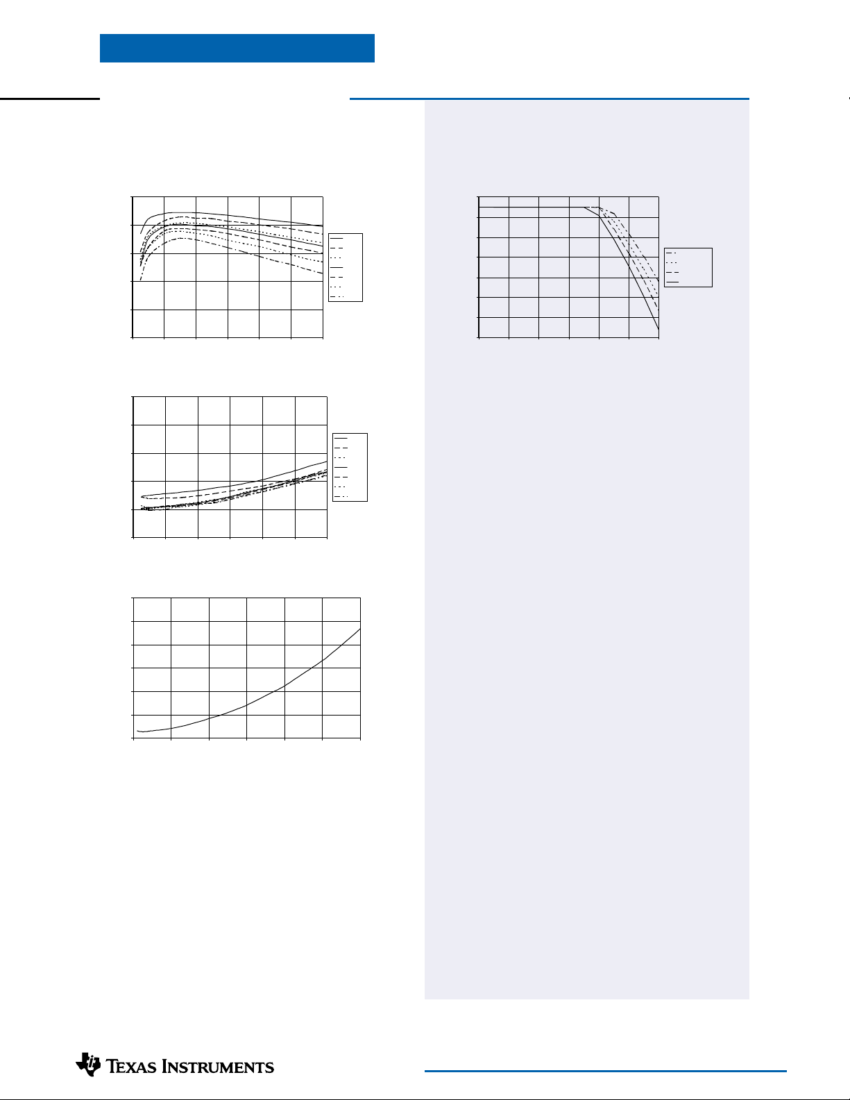
Efficiency vs Output Current
100
90
80
70
Efficiency - %
60
50
0123456
Ripple vs Output Current
50
40
30
20
Ripple - mV
10
Iout - Amps
SLTS201C – MAY 2003 – REVISED DECEMBER 2003
Safe Operating Area; Vin =5 V (See Note B)
All Output Voltages
90
V
OUT
3.3 V
2.5 V
2.0 V
1.8 V
1.5 V
1.2 V
1.0 V
V
OUT
3.3 V
2.5 V
2.0 V
1.8 V
1.5 V
1.2 V
1.0 V
80
70
60
50
40
Ambient Temperature (°C)
30
20
0123456
Iout (A
Airflow
400LFM
200LFM
100LFM
Nat Conv
0
0123456
Power Dissipation vs Output Current
3
2.5
2
1.5
Pd - Watts
1
0.5
0
0123456
Iout - Amps
Iout - Amps
Note A: Characteristic data has been developed from actual products tested at 25 °C. This data is considered typical data for the Converter.
Note B: SOA curves represent the conditions at which internal components are at or below the manufacturer’s maximum operating temperatures. Derating limits apply to
modules soldered directly to a 4 in.
×
4 in. double-sided PCB with 1 oz. copper.
For technical support and further information visit http://power.ti.com

Application Notes
PTH05000W
Capacitor Recommendations for the PTH05000W
Wide-Output Adjust Power Modules
Input Capacitor
The recommended input capacitor(s) is determined by
the 330 µF minimum capacitance and 300 mArms minimum ripple current rating.
Ripple current, less than 300 mΩ equivalent series resis-
tance (ESR), and temperature are the major considerations
when selecting input capacitors. Unlike polymer tantalum,
regular tantalum capacitors have a recommended mini-
mum voltage rating of 2 × (maximum DC voltage + AC
ripple). This is standard practice to ensure reliability.
For improved ripple reduction on the input bus, ceramic
capacitors
and achieve the minimum required capacitance.
Output Capacitors (Optional)
For applications with load transients (sudden changes in
load current), regulator response will benefit from an
external output capacitance. The recommended output
capacitance of 100 µF will allow the module to meet
its transient response specification (see product data sheet).
For most applications, a high quality computer-grade
aluminum electrolytic capacitor is adequate. These capacitors provide decoupling over the frequency range, 2 kHz
to 150 kHz, and are suitable for ambient temperatures
above 0 °C. For operation below 0 °C tantalum, ceramic
or Os-Con type capacitors are recommended. When using
one or more non-ceramic capacitors, the calculated equiva-
lent ESR should be no lower than 4 mΩ (7 mΩ using the
manufacturer’s maximum ESR for a single capacitor). A
list of preferred low-ESR type capacitors are identified
in Table 1-1.
Ceramic Capacitors
Above 150 kHz the performance of aluminum electrolytic
capacitors becomes less effective. To further improve the
reflected input ripple current
response, multilayer ceramic capacitors can also be added.
Ceramic capacitors have very low ESR and their resonant
frequency is higher than the bandwidth of the regulator.
When used on the output their combined ESR is not
critical as long as the total value of ceramic capacitance
does not exceed 300 µF. Also, to prevent the formation of
local resonances, do not place more than five identical ceramic capacitors in parallel with values of 10 µF or greater.
Tantalum Capacitors
Tantalum type capacitors can be used at both the input
and output, and are recommended for applications where
the ambient operating temperature can be less than 0 °C.
The AVX TPS, Sprague 593D/594/595 and Kemet T495/
[2]
may used to complement electrolytic types,
[2]
or the output transient
T510 capacitor series are suggested over many other
tantalum types due to their higher rated surge, power
dissipation, and ripple current capability. As a caution
many general purpose tantalum capacitors have considerably higher ESR, reduced power dissipation and lower
ripple current capability. These capacitors are also less
reliable as they have lower power dissipation and surge
current ratings. Tantalum capacitors that do not have a
stated ESR or surge current rating are not recommended
for power applications.
When specifying Os-Con and polymer tantalum capacitors
for the output, the minimum ESR limit will be encountered well before the maximum capacitance value is
reached.
Capacitor Table
Table 1-1 identifies the characteristics of capacitors from a
number of vendors with acceptable ESR and ripple current
(rms) ratings. The recommended number of capacitors
required at both the input and output buses is identified
for each capacitor type.
This is not an extensive capacitor list. Capacitors from other
vendors are available with comparable specifications. Those
listed are for guidance. The RMS ripple current rating and
ESR (at 100 kHz) are critical parameters necessary to insure
both optimum regulator performance and long capacitor life.
Designing for Very Fast Load Transients
The transient response of the DC/DC converter has been
characterized using a load transient with a di/dt of 1 A/µs.
The typical voltage deviation for this load transient is
given in the data sheet specification table using the
optional value of output capacitance. As the di/dt of a
transient is increased, the response of a converter’s regulation circuit ultimately depends on its output capacitor
decoupling network. This is an inherent limitation with
any DC/DC converter once the speed of the transient
exceeds its bandwidth capability. If the target application
specifies a higher di/dt or lower voltage deviation, the
requirement can only be met with additional output
capacitor decoupling. In these cases special attention
must be paid to the type, value and ESR of the capacitors
selected.
If the transient performance requirements exceed that
specified in the data sheet, the selection of output capacitors becomes more important. For further guidance
consult the separate application note, “Selecting Output
Capacitors for PTH Products in High-Performance Applications.”
For technical support and further information visit http://power.ti.com

Application Notes
continued
PTH05000 Series
Table 1-1: Input/Output Capacitors
)elytS(seireS
/epyT,rodneVroticapaC
gnikroW
egatloV)Fµ(eulaV
cinosanaP
)DMS(GW
)laidaR(MP
oynaS
)DMS(
)DMS(temeK
,025TmunimulAyloP
eugarpS-yahsiV
)DMS(munimulA-yloP,AW
)DMS(munimulA,CF
)DMS(munimulA,KF
)laidaR(munimulA,CF
noC–imehCdetinU
)DMS(mulA-yloP,AXP
)laidaR(noc-sO,SF
)laidaR(munimulA,ZXL
)DMS(numimulA,ZVM
)laidaR(munimulA-yloP,ASP
munimulAnocihciN
)DMS(noc-sO,PVS
)laidaR(noc-sO,PS
)DMS(remyloPpacsoP,EPT
SPTmulatnaTXVA
.mulA-yloPcinagrO,035T
)DMS(mulatnaT,D495
)DMS(mulatnaT,D595
)DMS(noc-sO,PVS49
)laidaR(noc-sO,AS49
)DMS(R5XcimareC,temeKV61
V01
V61
V61
V01
V01
V01
V61
V52
V3.6
V61
V01
V01
V01
V3.6
V01
V01
V01
V01
V01
V01
V3.6
V3,6
V3.6
033Fµ
033Fµ
033Fµ
033Fµ
033Fµ
Fµ033
Fµ033
Fµ033
Fµ033
Fµ033
Fµ033
Fµ093
Fµ074
Fµ033
Fµ033
Fµ033
Fµ033
Fµ033
Fµ033
Fµ033
Fµ033
Fµ033
01
74
.0530 Ω
051.0 Ω
061.0 Ω
711.0 Ω
420.0 Ω
520.0 Ω
021.0 Ω
071.0 Ω
800.0 Ω
051.0 Ω
061.0 Ω
520.0 Ω
510.0 Ω
520.0 Ω
01.00Ω
060.0 Ω
040.0 Ω
510.0 Ω
540.0 Ω
041.0 Ω
520.0 Ω
520.0 Ω
200.0 Ω
200.0 Ω
RSE.xaM
zHk001ta
scitsiretcarahCroticapaCytitnauQ
elppiR.xaM
C°58tatnerruC
)smrI(
Am0082
Am076
Am006
Am055
Am0773
Am0053
Am555
Am054
Am0805
Am076
Am064
Am0073
Am0054
Am0042
Am0011
Am0002
× W3.4 × H1.4
Am0021
Am0011
Am0041
Am0001
× W0.6 × H1.4
Am0033
Am0053
—esac0121
8× 9.6
01 × 2.01
8× 2.01
8× 5.11
01 × 7.7
01 × 5.01
8× 21
8× 01
8× 5.11
01 × 01
8× 5.11
01 × 5.01
L3.7 × W3.4
L3.7 × W7.5
× H0.4
01 × 5.01
eziSlacisyhP
)mm(
01 ×8
L3.7
L3.7
01 ×8
mm5223
tupnI
suB
1
1
1
1
1
1
1
1
1
1
1
1
1
1
1
1
1
1
1
1
1
1
]2[
1
]2[
1
tuptuO
suB
≤3
≤3
≤3
≤3
≤3
≤3
≤3
≤3
≤1
≤3
≤3
≤3
≤2
≤3
≤3
≤3
≤3
≤2
≤3
≤3
≤3
≤3
≤3
≤2
M033SF01
M074PS01
rebmuNrodneV
P121A1AWFEE
P133C1CFVEE
P133C1KFVEE
133A1CFUEE
PT08JM133CV01AXP
LL21x8M133BV61ZXL
PT01HM133CV52ZVM
11HM093BV3.6ASP
SG1RNM133C1GWU
HHM133A1MPU
XM033PVS01
LM033EPT6
0010R010M733VSPT
0600R010M733VSPT
SA010M733X025T
SA010M733X035T
T2R0100X733D495
T2D0100X733D595
8F3R60X733PVS49
PBF3R60X733AS49
CAP4M601C0121C
CAP9K674C0121C
cimareC,ataruMR5X)DMS(V3.6
cimareC,KDTR5X)DMS(V3.6
[1] A total capacitance of 300 µF is acceptable based on the surge current capability of ceramic capacitors.
[2] A ceramic capacitor may be used to complement electrolytic types at the input to further reduce high-frequency ripple current.
V3.6
V61
V61
V3.6
V61
V61
001
74
22
01
001
74
22
01
200.0 Ω —esac0121
200.0 Ω —esac0121
mm5223
mm5223
]1[
3
]2[
1
≤2
]2[
1
≤3
]2[
1
≤3
]1[
3
]2[
1
≤2
]2[
1
≤3
]2[
1
≤3
For technical support and further information visit http://power.ti.com
1≤
1≤
M701J06RE23MRG
M674J06RE23MRG
K622C16RE23MRG
K601C16RD23MRG
TM701J0R5X5223C
TM674J0R5X5223C
TM622C1R5X5223C
TM601C1R5X5223C

Application Notes
PTH05000W
Adjusting the Output Voltage of the PTH05000W
Wide-Output Adjust Power Modules
The Vo Adjust control (pin 4) sets the output voltage of
the PTH05000Wproduct. The adjustment range is
from 0.9 V to 3.6 V. The adjustment method requires
the addition of a single external resistor, R
, that must
set
be connected directly between the Vo Adjust and GND
pins 1. Table 2-1 gives the preferred value of the external
resistor for a number of standard voltages, along with the
actual output voltage that this resistance value provides.
For other output voltages the value of the required resistor
can either be calculated using the following formula, or
simply selected from the range of values given in Table 2-2.
Figure 2-1 shows the placement of the required resistor.
R
= 10 kΩ ·
set
Table 2-1; Preferred Values of R
V
(Standard) R
out
3.3 V 475 Ω 3.298V
2.5 V 2.32 kΩ 2.502 V
2 V 4.87 kΩ 1.999 V
1.8 V 6.65 kΩ 1.801 V
1.5 V 11.5 kΩ 1.504 V
1.2 V 26.1 kΩ 1.204 V
1 V 84.5 kΩ 1.001 V
0.9 V Open 0.9 V
Figure 2-1; Vo Adjust Resistor Placement
0.891 V
V
– 0.9 V
out
for Standard Output Voltages
set
(Pref’d Value) V
set
– 3.24 kΩ
(Actual)
out
Table 2-2; Output Voltage Set-Point Resistor Values
Va Req’dR
0.900 Open
0.925 353 kΩ
0.950 175 kΩ
0.975 116 kΩ
1.000 85.9 kΩ
1.025 68.0 kΩ
1.050 56.2 kΩ
1.075 47.7 kΩ
1.100 41.3 kΩ
1.125 36.4 kΩ
1.150 32.4 kΩ
1.175 29.2 kΩ
1.200 26.5 kΩ
1.225 24.2 kΩ
1.250 22.2 kΩ
1.275 20.5 kΩ
1.300 19.0 kΩ
1.325 17.7 kΩ
1.350 16.6 kΩ
1.375 15.5 kΩ
1.400 14.6 kΩ
1.425 13.7 kΩ
1.450 13.0 kΩ
1.475 12.3 kΩ
1.50 11.6 kΩ
1.55 10.5 kΩ
1.60 9.49 kΩ
1.65 8.64 kΩ
1.70 7.90 kΩ
1.75 7.24 kΩ
1.80 6.66 kΩ
1.85 6.14 kΩ
1.90 5.67 kΩ
1.95 5.25 kΩ
set
Va Req’dR
2.00 4.86 kΩ
2.05 4.51 kΩ
2.10 4.19 kΩ
2.15 3.89 kΩ
2.20 3.61 kΩ
2.25 3.36 kΩ
2.30 3.12 kΩ
2.35 2.90 kΩ
2.40 2.70 kΩ
2.45 2.51 kΩ
2.50 2.33 kΩ
2.55 2.16 kΩ
2.60 2.00 kΩ
2.65 1.85 kΩ
2.70 1.71 kΩ
2.75 1.58 kΩ
2.80 1.45 kΩ
2.85 1.33 kΩ
2.90 1.22 kΩ
2.95 1.11 kΩ
3.00 1.00 kΩ
3.05 904 Ω
3.10 810 Ω
3.15 720 Ω
3.20 634 Ω
3.25 551 Ω
3.30 473 Ω
3.35 397 Ω
3.40 324 Ω
3.45 254 Ω
3.50 187 Ω
3.55 122 Ω
3.60 60 Ω
set
4
Adj
V
V
IN
Inhibit
GND
For technical support and further information visit http://power.ti.com
+
C
IN
330µF
(Required)
2
V
IN
PTH05000W
3
O
V
O
GNDInhibit
1
R
SET
0.1 W, 1 %
5
V
OUT
Notes:
1. Use a 0.1 W resistor. The tolerance should be 1 %,
with a temperature stability of 100 ppm/°C (or better).
+
C
100µF
(Optional)
OUT
GND
Place the resistor as close to the regulator as possible.
Connect the resistor directly between pins 4 and 1
using dedicated PCB traces.
2. Never connect capacitors from V
. Any capacitance added to the Vo Adjust pin will affect
V
out
Adjust to either GND or
o
the stability of the regulator.

Application Notes
PTH03000 & PTH05000 Series
Power-Up Characteristics
When configured per their standard application, the
PTH03000 and PTH05000 series of power modules will
produce a regulated output voltage following the application of a valid input source voltage. During power up,
internal soft-start circuitry slows the rate that the output
voltage rises, thereby limiting the amount of in-rush
current that can be drawn from the input source. The
soft-start circuitry introduces a short time delay (typically 10 ms) into the power-up characteristic. This is
from the point that a valid input source is recognized.
Figure 3-1 shows the power-up waveforms for a PTH05000W
(5-V input), with the output voltage set point adjusted for a
2-V output. The waveforms were measured with a 5-A
resistive load. The initial rise in input current when the
input voltage first starts to rise is the charge current drawn
by the input capacitors.
Figure 3-1
Vin (2 V/Div)
Vo (1 V/Div)
Output On/Off Inhibit
For applications requiring output voltage on/off control,
the PTH03000W & PTH05000W power modules incorporate an output on/off Inhibit control (pin 3). The
inhibit feature can be used wherever there is a requirement for the output voltage from the regulator to be
turned off.
The power module functions normally when the Inhibit
pin is left open-circuit, providing a regulated output
whenever a valid source voltage is connected to V
in
with
respect to GND.
Figure 3-2 shows the typical application of the inhibit
function. Note the discrete transistor (Q
). The Inhibit
1
control has its own internal pull-up to Vin potential. An
open-collector or open-drain device is recommended to
control this input.
Turning Q
pin and disables the output of the module. If Q
on applies a low voltage to the Inhibit control
1
is then
1
turned off, the module will execute a soft-start power-up
sequence. A regulated output voltage is produced within
20 msec. Figure 3-3 shows the typical rise in the output voltage, following the turn-off of Q
corresponds to the fall in the waveform, Q1 Vgs. The
Q
1
. The turn off of
1
waveforms were measured with a 5-A resistive load.
Figure 3-2
Iin (2 A/Div)
HORIZ SCALE: 5 ms/Div
Current Limit Protection
The PTHxx000W modules protect against load faults
with a continuous current limit characteristic. Under a
load fault condition the output current cannot exceed
the current limit value. Attempting to draw current that
exceeds the current limit value causes the output voltage
to be progressively reduced. Current is continuously
supplied to the fault until it is removed. Upon removal of
the fault, the output voltage will promptly recover.
Thermal Shutdown
Thermal shutdown protects the module’s internal circuitry
against excessively high temperatures. A rise in temperature may be the result of a drop in airflow, a high ambient
temperature, or a sustained current limit condition. If
the junction temperature of the internal components
exceed 150 °C, the module will shutdown. This reduces
the output voltage to zero. The module will start up
automatically, by initiating a soft-start power up when
the sensed temperature decreases 10 °C below the thermal
shutdown trip point.
VIN =5 V
Inhibit
GND
Figure 3-3
HORIZ SCALE: 5 ms/Div
+
C
IN
330 µF
(Required)
2
Q
1
BSS138
V
IN
PTH05000W
3
4
Adj
V
O
5
V
O
GNDInhibit
1
4k87
0.1 W, 1 %
+
V
C
OUT
100 µF
(Optional)
GND
Vo (1 V/Div)
Q1 Vgs
(10 V/Div)
O
=2 V
L
O
A
D
For technical support and further information visit http://power.ti.com

Application Notes
PTH05000W
PTH05000W Startup with Output Pre-Bias
A pre-bias startup condition occurs as a result of an external
voltage being present at the output of the power module
prior to its output voltage rising. This often occurs in
complex digital systems when current from another power
source is backfed through a dual-supply logic component
such as an FPGA or ASIC. Another path might be via
clamp diodes (to a higher supply voltage) as part of a
sequential power-up arrangement.
An output prebias can cause problems with power modules
that incorporate synchronous rectifiers. This is because
under most operating conditions, they can sink as well as
source ouput current. Although the PTH05000W (5-V
input) power module can sink current under normal operation, it will not do so during startup. 1 This is true as
long as certain conditions are maintained. 2 Figure 3-1
shows an application schematic that demonstrates this
capability. Figure 3-2 shows the waveforms of the circuit
after input power is applied. Note that the module’s output current (Io) is never negative. Only positive current
is sourced. This occurs when the output voltage is raised
above that which is backfed from the 5-V input supply, via
the diodes D1 through D4.
3
Notes
1. Start up includes both the application of a valid input
source voltage, or the removal of a ground signal from
the Inhibit* control (pin 3) with a valid input source
applied. The output of the regulator is effectively off
(tri-state), during the period that the Inhibit* control is
held low.
2. To ensure that the regulator does not sink current, the
input voltage
output voltage
must always be greater or equal to the
throughout the power-up and power-down
sequence.
3. If during power up, the backfeeding source is greater
than the module’s set-point voltage, the module’s
output voltage will remain higher than its set point.
The output will remain out of regulation until the backfeeding source is either reduced in voltage or removed.
Figure 3-2; Start-up with Output Pre-Bias
Vin (1 V/Div)
Vo (1 V/Div)
Io (2 A/Div)
HORIZ SCALE: 5 ms/Div
Figure 3-1; Schematic Demonstrating Startup with Output Pre-Bias
- D
D
1
4
MUR460
VIN =5 V
Inhibit
GND
+
C
330 µF
(Required)
2
IN
V
IN
PTH05000W
3
GNDInhibit
1
4
Adj
V
O
2k32
0.1 W, 1 %
5
V
O
+
V
=2.5 V
O
C
OUT
100 µF
(Optional)
L
Ω
0.55
O
A
Resistive
D
GND
For technical support and further information visit http://power.ti.com
PACKAGE OPTION ADDENDUM
www.ti.com
12-Jan-2006
PACKAGING INFORMATION
Orderable Device Status
PTH05000WAD ACTIVE DIP MOD
(1)
Package
Type
Package
Drawing
Pins Package
Qty
Eco Plan
EUS 5 56 Pb-Free
ULE
PTH05000WAH ACTIVE DIP MOD
EUS 5 56 Pb-Free
ULE
PTH05000WAS ACTIVE DIP MOD
EUT 5 49 TBD Call TI Level-1-235C-UNLIM
ULE
PTH05000WAST ACTIVE DIP MOD
EUT 5 250 TBD Call TI Level-1-235C-UNLIM
ULE
PTH05000WAZ ACTIVE DIP MOD
EUT 5 49 Pb-Free
ULE
PTH05000WAZT ACTIVE DIP MOD
EUT 5 250 Pb-Free
ULE
(1)
The marketing status values are defined as follows:
ACTIVE: Product device recommended for new designs.
LIFEBUY: TI has announced that the device will be discontinued, and a lifetime-buy period is in effect.
NRND: Not recommended for new designs. Device is in production to support existing customers, but TI does not recommend using this part in
a new design.
PREVIEW: Device has been announced but is not in production. Samples may or may not be available.
OBSOLETE: TI has discontinued the production of the device.
(RoHS)
(RoHS)
(RoHS)
(RoHS)
(2)
Lead/Ball Finish MSL Peak Temp
Call TI N / A for Pkg Type
Call TI N / A for Pkg Type
Call TI Level-3-260C-168HR
Call TI Level-3-260C-168HR
(3)
(2)
Eco Plan - The planned eco-friendly classification: Pb-Free (RoHS), Pb-Free (RoHS Exempt), or Green (RoHS & no Sb/Br) - please check
http://www.ti.com/productcontent for the latest availability information and additional product content details.
TBD: The Pb-Free/Green conversion plan has not been defined.
Pb-Free (RoHS): TI's terms "Lead-Free" or "Pb-Free" mean semiconductor products that are compatible with the current RoHS requirements
for all 6 substances, including the requirement that lead not exceed 0.1% by weight in homogeneous materials. Where designed to be soldered
at high temperatures, TI Pb-Free products are suitable for use in specified lead-free processes.
Pb-Free (RoHS Exempt): This component has a RoHS exemption for either 1) lead-based flip-chip solder bumps used between the die and
package, or 2) lead-based die adhesive used between the die and leadframe. The component is otherwise considered Pb-Free (RoHS
compatible) as defined above.
Green (RoHS & no Sb/Br): TI defines "Green" to mean Pb-Free (RoHS compatible), and free of Bromine (Br) and Antimony (Sb) based flame
retardants (Br or Sb do not exceed 0.1% by weight in homogeneous material)
(3)
MSL, Peak Temp. -- The Moisture Sensitivity Level rating according to the JEDEC industry standard classifications, and peak solder
temperature.
Important Information and Disclaimer:The information provided on this page represents TI's knowledge and belief as of the date that it is
provided. TI bases its knowledge and belief on information provided by third parties, and makes no representation or warranty as to the
accuracy of such information. Efforts are underway to better integrate information from third parties. TI has taken and continues to take
reasonable steps to provide representative and accurate information but may not have conducted destructive testing or chemical analysis on
incoming materials and chemicals. TI and TI suppliers consider certain information to be proprietary, and thus CAS numbers and other limited
information may not be available for release.
In no event shall TI's liability arising out of such information exceed the total purchase price of the TI part(s) at issue in this document sold by TI
to Customer on an annual basis.
Addendum-Page 1


IMPORTANT NOTICE
Texas Instruments Incorporated and its subsidiaries (TI) reserve the right to make corrections, modifications,
enhancements, improvements, and other changes to its products and services at any time and to discontinue
any product or service without notice. Customers should obtain the latest relevant information before placing
orders and should verify that such information is current and complete. All products are sold subject to TI’s terms
and conditions of sale supplied at the time of order acknowledgment.
TI warrants performance of its hardware products to the specifications applicable at the time of sale in
accordance with TI’s standard warranty. Testing and other quality control techniques are used to the extent TI
deems necessary to support this warranty. Except where mandated by government requirements, testing of all
parameters of each product is not necessarily performed.
TI assumes no liability for applications assistance or customer product design. Customers are responsible for
their products and applications using TI components. To minimize the risks associated with customer products
and applications, customers should provide adequate design and operating safeguards.
TI does not warrant or represent that any license, either express or implied, is granted under any TI patent right,
copyright, mask work right, or other TI intellectual property right relating to any combination, machine, or process
in which TI products or services are used. Information published by TI regarding third-party products or services
does not constitute a license from TI to use such products or services or a warranty or endorsement thereof.
Use of such information may require a license from a third party under the patents or other intellectual property
of the third party, or a license from TI under the patents or other intellectual property of TI.
Reproduction of information in TI data books or data sheets is permissible only if reproduction is without
alteration and is accompanied by all associated warranties, conditions, limitations, and notices. Reproduction
of this information with alteration is an unfair and deceptive business practice. TI is not responsible or liable for
such altered documentation.
Resale of TI products or services with statements different from or beyond the parameters stated by TI for that
product or service voids all express and any implied warranties for the associated TI product or service and
is an unfair and deceptive business practice. TI is not responsible or liable for any such statements.
Following are URLs where you can obtain information on other Texas Instruments products and application
solutions:
Products Applications
Amplifiers amplifier.ti.com Audio www.ti.com/audio
Data Converters dataconverter.ti.com Automotive www.ti.com/automotive
DSP dsp.ti.com Broadband www.ti.com/broadband
Interface interface.ti.com Digital Control www.ti.com/digitalcontrol
Logic logic.ti.com Military www.ti.com/military
Power Mgmt power.ti.com Optical Networking www.ti.com/opticalnetwork
Microcontrollers microcontroller.ti.com Security www.ti.com/security
Telephony www.ti.com/telephony
Video & Imaging www.ti.com/video
Wireless www.ti.com/wireless
Mailing Address: Texas Instruments
Post Office Box 655303 Dallas, Texas 75265
Copyright 2006, Texas Instruments Incorporated
 Loading...