

Page 1
µ
查询PT7743N供应商
PT7615—5V
20-A Low-Voltage Programmable
Integrated Switching Regulator
Description
The PT7615 power module is a 20-A
fully integrated switching regulator (ISR)
housed in a 27-pin aluminum SIP package.
Operating from a 5V-input bus, the
PT7615 produces a tightly regulated
supply voltage that is programmable over
the range, 1.075V to 1.85V. The output
voltage is selected via a 5-bit code. The
code adjusts the voltage in steps of 25mV
and is VRM 9.0 compatible.
This regulator is most suitable for
applications that employ microprocessor
and DSP products that require core supply
voltages as low as 1.075V.
The PT7615 includes a Shutdown
control, Differential Remote Sense, and
Short-Circuit Protection.
Features
• Single-Device: +5V Input
• 20A Output
• 5-bit Programmable:
1.075V to 1.85V (25mV Steps)
• VRM 9.0 Compatible
• High Efficiency (87%)
Ordering Information
PT7615o = 1.075 to 1.85Volts
PT7743o = 20A Booster
PT Series Suffix
Case/Pin Order Package
Configuration Suffix Code
Vertical N (EHD)
Horizontal A (EHA)
SMD C (EHC)
(Reference the applicable package code drawing for the dimensions and PC board layout)
(PT1234x )
(Revised 12/13/2001)
• Differential Remote Sense
• Short-Circuit Protection
• Compatible with PT7743
20A “Current Booster”
Pin-Out Information
Pin Function
1 VID0
2 VID1
3 VID2
4 VID3
5 STBY *
6 VID4
7V
in
8V
in
9V
in
10 V
in
11 V
in
12 Remote Sense (–)
13 GND
14 GND
For STBY* pin: open =output enabled
ground =output disabled.
Pin Function
15 GND
16 GND
17 GND
18 GND
19 GND
20 V
21 V
22 V
23 V
24 V
25 V
26 Remote Sense (+)
27 Sync Out
SLTS163
out
out
out
out
out
out
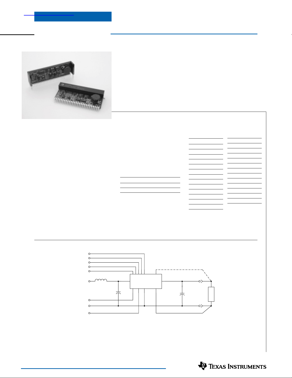
Standard Application
For technical support and more information, see inside back cover or visit www.ti.com
VID0
VID1
VID2
VID3
VID4
V
IN
SYNC OUT
GND
STBY*
PROGRAMMING PINS
L1
H
1
7-11
+
C
IN
4321 26
6
PT7615
27
REMOTE SENSE(+)
20-25
125 13-19
REMOTE SENSE(–)
V
OUT
+
C
OUT
GND
Cin= Required 1500µF electrolytic
C
= Required 330µF electrolytic
out
L1= Optional 1µH input choke
L
O
A
D
Page 2
PT7615—5V
20-A Low-Voltage Programmable
Integrated Switching Regulator
Programming Information
VID3 VID2 VID1 VID0 Vout Vout
1111 1.075V 1.475V
1110 1.100V 1.500V
1101 1.125V 1.525V
1100 1.150V 1.550V
1011 1.175V 1.575V
1010 1.200V 1.600V
1001 1.225V 1.625V
1000 1.250V 1.650V
0111 1.275V 1.675V
0110 1.300V 1.700V
0101 1.325V 1.725V
0100 1.350V 1.750V
0011 1.375V 1.775V
0010 1.400V 1.800V
0001 1.425V 1.825V
0000 1.450V 1.850V
Logic 0 = Pin 12 potential (Rem Sense Gnd)
Logic 1 = Open circuit (no pull-up resistors)
VID4 may not be changed while the unit is operating.
VID4=1 VID4=0
Specifications (Unless otherwise stated, T
=25°C, Vin =5V, Cin =1,500µF, C
a
20-A Programmable SIP Family
Product Voltage Description Method Range
PT7709 5V VID 5-Bit 1.3V– 3.5V
PT7708 3.3V VID 4-Bit 1.3V– 2.05V
PT7615 5V VID 5-Bit 1.075V–1.85V
PT7742 3.3V Booster — —
PT7743 5V Booster — —
out
Input Adjust Output
=330µF, and Io =Iomax)
PT7615
Characteristics Symbols Conditions Min Typ Max Units
Output Current Io Ta = +60°C, 200 LFM, pkg N 0.1
Ta = +25°C, natural convection 0.1
(1)
—20A
(1)
—20
Input Voltage Range Vin Over Io range 4.5 — 5.5 V
Set-Point Voltage Tolerance Vo tol — ±10 ±25
Temperature Variation Reg
temp
–40°C ≤Ta ≤ +85°C — ±1.5 — %V
(2)
mV
Line Regulation Regline Over Vin range — ±5 ±10 mV
Load Regulation Regload Over Io range — ±5 ±10 mV
Total Output Voltage Variation ∆V
Efficiency η I
tol Set-point, line, load
o
–40°C ≤Ta ≤ +85°C
o = 10A Vo = 1.8V — 87 —
I
o = 20A Vo = 1.8V — 82 —
—±2±3%V
o = 1.5V — 84 — %
V
Vo = 1.2V — 81 —
o = 1.5V — 79 — %
V
Vo = 1.2V — 75 —
Vo Ripple (pk-pk) Vr 20MHz bandwidth — 40 — mV
Transient Response ttr 1A/µs load step, 10A and 20A — 50 — µSec
Vos Vo over/undershoot — ±100 — mV
Short Circuit Threshold Isc (pk) — 32 — A
Switching Frequency ƒs Over Vin range 300 350 400 kHz
STBY* Input Requirements Referenced to GND
Input High Voltage V
Input Low Voltage V
Input Low Current I
IH
IL
IL
Pin 5 to GND — 0.3 — mA
2.0 —
-0.2 — 0.8
Open
(3)
V
Standby Input Current Iin standby Pin 5 to GND — 30 — mA
External Capacitance C
out
Operating Temperature Range Ta Over Vin Range –40 — +85
330
(4)
— 15,000 µF
(5)
°C
Storage Temperature Ts — -40 — +125 °C
Mechanical Shock Per Mil-STD-883D, Method 2002.3
Mechanical Vibration Per Mil-STD-883D, Method 2007.2, — 10 — G’s
1 msec, Half Sine, mounted to a fixture — 500 — G’s
20-2000 Hz, Soldered in a PC board
Weight — Vertical/Horizontal — 36 — grams
Flammability — Materials meet UL 94V-0
Notes:
(1) ISR-will operate down to no load with reduced specifications.
(2) If the remote sense is not used, pin 12 must be connected to pin 13 for optimum output voltage accuracy.
(3) The STBY* control (pin 5) has an internal pull-up. If it is left open-circuit, the module will operate when input power is applied. A low-leakage (<1µA)
MOSFET must be used to control this pin. The open-circuit voltage may be as high as Vin.
(4) For operation below 0°C, Cin and Cout must have stable characteristics. Use either low ESR tantalum or Oscon® capacitors.
(5) See safe Operating Area curves or consult factory for the appropriate derating.
External Capacitors:
which must be rated for a minimum of 1.4Arms of ripple current. For transient or dynamic load applications, additional capacitance may be required. For further
information refer to the application note regarding capacitor selection for this product.
Input Filter:
The PT7615 require a minimum output capacitance of 330µF for proper operation. The PT7615 also requires an input capacitance of 1500µF,
An input filter inductor is optional for most applications. The inductor must be sized to handle 10ADC with a typical value of 1µH.
o
o
pp
For technical support and more information, see inside back cover or visit www.ti.com
Page 3
PT7615—5V
)
)
)
)
)
20 Amp Low Voltage Programmable
Integrated Switching Regulator
T ypical Characteristics
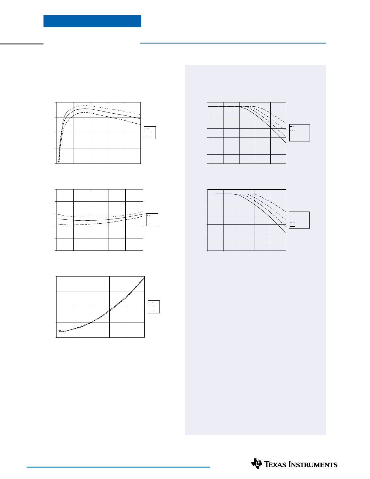
PT7615 Characteristic Data, Vin =5.0 (See Note A)
Efficiency vs Output Current
90.0
80.0
70.0
Efficiency - %
60.0
50.0
048121620
Ripple vs Output Current
50
40
30
20
Ripple - mV
10
0
048121620
Iout (A
Iout (A
V
OUT
1.8
1.5
1.2
V
OUT
1.8
1.5
1.2
PT7615 Safe Operating Area, Vin =5.0 (See Note B)
PT7615; Vo =1.2V
90
80
70
60
50
40
Ambient Temperature (°C)
30
20
0 4 8 12 16 20
PT7615; Vo =1.8V
90
80
70
60
50
40
Ambient Temperature (°C)
30
20
0 4 8 12 16 20
Iout (A
Iout (A
Airflow
200LFM
120LFM
60LFM
Nat conv
Airflow
200LFM
120LFM
60LFM
Nat conv
Power Dissipation vs Output Current
8
6
4
Pd - Watts
2
0
048121620
Note A:
All characteristic data in the above graphs has been developed from actual products tested at 25°C. This data is considered typical for the ISR.
Note B:
SOA curves represent operating conditions at which internal components are at or below manufacturer’s maximum rated operating temperatures.
Iout (A
V
OUT
1.8
1.5
1.2
For technical support and more information, see inside back cover or visit www.ti.com
Page 4

Application Notes
PT7708/09, PT7615, PT7742/PT7743
Capacitor Recommendations for 20-A
Programmable Switching Regulators
Input Capacitors
The recommended input capacitance is determined by the
1.4 ampere minimum ripple current rating and 1500µF
minimum capacitance. Capacitors listed below must be
rated for a minimum of two times (2×) the input voltage
with +5V operation. Ripple current and ≤100mΩ ESR
(equivalent series resistance) values are the major considerations along with temperature when selecting the proper
capacitor.
Output Capacitors
The minimum required output capacitance is 330µF with a
maximum ESR less than or equal to 100mΩ. Failure to
observe this requirement may lead to regulator instability
or oscillation. Electrolytic capacitors have poor ripple
performance at frequencies greater than 400kHz, but
excellent low frequency transient response. Above the
ripple frequency ceramic decoupling capacitors are necessary to improve the transient response and reduce any
microprocessor high frequency noise components apparent
during higher current excursions. Preferred low ESR type
capacitor part numbers are identified in the Table 1 below.
Table 1 Capacitors Characteristic Data
Tantalum Characteristics
Tantalum capacitors with a minimum 10-V rating are
recommended on the output bus, but only the AVX TPS
Series, Sprague 594/595 Series, or Kemet T495/T510
Series. These AVX, Sprague, and Kemet capacitors are
specified over other types due to their higher surge current,
excellent power dissipation and ripple current ratings.
As a caution, the TAJ Series by AVX is not recommended.
This series exhibits considerably higher ESR, reduced
power dissipation and lower ripple current capability.
The TAJ series is also less reliable compared to the TPS
series when determining power dissipation capability.
Capacitor Table
Table 1 identifies the characteristics of capacitors from a
number of vendors with acceptable ESR and ripple current
(rms) ratings. The suggested minimum quantities per
regulator for both the input and output buses are identified.
This is not an extensive capacitor list. Capacitors from
other vendors are available with comparible specifications.
The RMS ripple current rating and ESR (Equivalent Series
Resistance at 100kHz) are the critical parameters necessary
to insure both optimum regulator performance and long
capacitor life.
roticapaC
scitsiretcarahCroticapaCytitnauQ
/rodneV
seireS
gnikroW
egatloV
cinosanaP
)TMS(CF
)laidaR(CF
detinU
noC-imehC
seireSVFL
nocihciN
seireSLP
seireSMP
nocsO
)laidaR(SS
)TMS(VS
XVA
mulatanaT
seireS-SPT
eugarpS
mulatnaT
D495/D595
temeK
mulatnaT
594T/015T
seireS
BPT
Note:
(N/R) is not recommended for this application, due to extremely low Equivalent Series Resistance (ESR)
V61
V53
V01
V61
V52
V61
V61
V01
V01
V52
V01
V01
V01
V01
V01
V01
V01
V01
pacsoPoynaS
V0102240.0 Ω Am0003xL2.7
0022
033
065
0081
033
0022
074
086
0081
033
033
033
033
033
033
086
033
022
)Fµ(eulaVtnelaviuqE)RSE(
830.0 Ω
560.0 Ω
090.0 Ω
230.0 Ω
480.0 Ω
830.0 Ω
480.0 ÷Ω 240.0=2 Ω
090.0 Ω
440.0 Ω
590.0 Ω
520.0 ÷Ω 600.0=4 Ω
20.0 ÷Ω 500.0=4 Ω
1.0 ÷Ω 20.0=5 Ω
60.0 Ω
540.0 ÷Ω 110.0=4 Ω
90.0 Ω
530.0 Ω
70.0 ÷Ω 530.0=2 Ω
ecnatsiseRseireS
mumixaMC°501
elppiR
)smrI(tnerruC
Am0002
Am5021
Am557
Am0002
Am528
Am0361
2xAm528
Am077
Am0241
Am057
Am0089>
Am0089>
Am0053
Am6281
Am0054>
Am0661>
Am0002
Am0002>
lacisyhP
)mm(eziS
5.61x81
5.61x5.21
5.21x01
51x81
61x01
02x61
61x01
51x01
51x61
51x01
5.01x01
6.21x3.01
xL3.7
xW3.4
H1.4
xL3.7
xW7.5
H0.4
L3.7xW3.4
H0.4x
xW3.4
H1.3
tupnI
suB
1
1
1
1
4
4
5
5
5
2
5
6
62 M022BPT01
tuptuO
suB
1
1
1
1
1
1
1
1
1
1
R/N
)etoN(
1
1
1
1
1
2
rebmuNrodneV
N222C1CFVEE
QL133V1CFVEE
165A1CFUEE
S281C1CFUEE
LL61X01M133BV52VXL
LL02X61M222BV61VXL
LL61X01M174BV61VXL
6HHM186A1LPU
6HHM281A1LPU
6HPM133E1LPU
M033SS01
M033VS01
0010R010M733VSPT
0600R010M733VSPT
T2R0100X733D495
T2R0100X786D595
)tnuoMecafruS(
SA010M733X015
SA010M722X594T
)tnuoMecafruS(
)tnuoMecafruS(
For technical support and more information, see inside back cover or visit www.ti.com
Page 5

Application Notes
y
)
)
continued
PT7708/09, PT7615
Using the Standby Function on 20-A
Programmable Switching Regulators
For applications requiring On/Off control of the output
voltage, the 20-A programmable regulators incorporate
a standby function. This feature may be used for powerup/shutdown sequencing, or to change the output voltage
while input power is applied. See related note: “Pin-Coded
Output Voltage Adjustment of 20-A Programmable Regulators”
The standby function is provided by the STBY* control,
pin 5. If pin 5 is left open-circuit the regulator operates
normally, providing a regulated output whenever a valid
supply voltage is applied to V
(pins 7-11) with respect to
in
GND (pins 13-19). Connecting pin 5 to ground 1 will set
2
the regulator output to zero volts
. This places the regulator in standby mode, and reduces the input current to
typcially 30mA (60mA max). If a ground signal is applied
to pin 5 prior to power-up, the regulator output will be
held at zero volts during the period that input power is
applied.
The standby input must be controlled with an opencollector (or open-drain) discrete transistor (See Figure 1).
Table 1 gives the input requirements.
Table 1 Standby Control Input Requirements
Parameter Min Typ Max
Enable 2V Open Cct.
Disable –0.2V 0.8V
I
stby (low)
Vstby (o/c) V
in
(1, 2)
1
0.5mA
Figure 1
64321 26
5V
Inhibit
COM
VID4 - VID0
7-11
PT770x/PT761x
S
nch
STBY
Out
27
+
C
in
Q1
BSS138
GND
Rem Sns (+)
VoVin
Rem Sns (–)
125 13-19
20-25
C
Vo =3.3V
L
+
out
O
A
D
COM
Turn-On Time: Turning Q1 in Figure 1 off, removes the
low-voltage signal at pin 5 and enables the output.
Following a delay of approximately 10ms, the regulator
3
output voltage rises to full regulation within 30ms
.
Figure 2 shows the typical output voltage waveform of a
PT7709 following the turn-off of Q1 at time t =0 secs.
The output voltage is set to 3.3V by connecting VID0
(pin 1), VID2 (pin 3), and VID3 (pin 4) to the ‘Rem
*
Sns (–)’, (pin 12)
. The waveform was measured with a
+5V input source voltage, and 10-A resistive load.
Figure 2
Notes:
1. The Standby input must be controlled using an opencollector (or open-drain) discrete transistor.
Do Not use a
pull-up resistor. The control input has an open-circuit
voltage equal to V
. To set the regulator output to zero,
in
the control pin must be “pulled” to less than 0.8Vdc with a
0.5mA sink to ground.
2. When placed in the standby mode, the regulator output
discharges the output capacitance with a low impedance to
ground.
3. The turn-off time of Q1, or rise time of the standby input
is not critical with these regulators. Turning Q
off slowly,
1
over periods up to 100ms, will not affect regulator operation.
A slow turn-off time will merely increase both the initial
delay and rise-time of the output voltage.
For technical support and more information, see inside back cover or visit www.ti.com
Vo (2V / Div
Iin 10A / Div
0 5 10 15 20 25 30
t (milli - secs)
*
Consult the data sheet for details on other VID codes.
Page 6

Application Notes
PT7708/09, PT7615
Pin-Coded Output Voltage Adjustment of
20-A Programmable Regulators
The 20-A family of programmable ISRs incorporate a pincoded control to adjust the output voltage. This feature
uses the control pins VID0–VID4 (pins 1–6). When
the control pins are left open-circuit, the ISR output
regulates at its default output voltage. Each control pin
is internally connected to a precision resistor, which
when grounded applies a weighted change to the output
voltage. By selectively grounding VID0–VID4, the output
voltage of these ISRs can be programmed in incremental
steps over the module’s output voltage range. The program
codes and output voltage range offered by these ISRs are
compatible with the Voltage ID specifications defined by
Intel Corporation for VRMs (voltage regulator modules). The codes are used by both the Pentium® and
Athlon® microprocessors. Refer to Figure 1 for the
connection schematic, and the respective device Data Sheet
for the programming code information.
Notes:
1. The programming convention is as follows:
Logic 0: Connect to pin 12 (Remote Sense Ground).
Logic 1: Open circuit/open drain (See notes 2, & 4)
2. Do not connect pull-up resistors to the voltage
programming pins.
3. Use pin 12 (Remote Sense Ground) as the logic “0”
reference. While the regular ground (pins 13-19) can also
be used for programming, doing so will degrade the load
reglation of the product. If the remote sense ground is
not used, pin 12 must be connected to pin 13 for
optimum output voltage accuracy.
4. If active devices are used to ground the voltage control
pins, low-level open drain MOSFET devices should be
used over bipolar transistors. The inherent Vce(sat) in
bipolar devices introduces errors in the device’s internal
divider network. Discrete transistors such as the BSS138,
2N7002, or IRLML2402 are examples of appropriate
devices.
Active Voltage Programming:
Special precautions should be taken when making changes
to the voltage control progam code while the unit is
powered. It is highly recommended that the ISR be either
powered down or held in standby. Changes made to the
program code while V
is enabled induces high current
out
transients through the device. This is the result of the
electrolytic output capacitors being either charged or
discharged to the new output voltage set-point. The
transient current can be minimized by making only incremental changes to the binary code, i.e. one LSB at a
time. A minimum of 100µs settling time between each
program state is also recommended. Making nonincremental changes to VID3 or VID4 while the output
is enabled is discouraged. The transients induced can
overstress the device. If the program code cannot be
asserted priot to power-up, pull pin 5 (STBY) control to
GND during the period that the input voltage is applied
to Vin. Releasing pin 5 will then allow the device to perform a soft-start to the programmed voltage. For more
information on the use of the Standby function, consult
the related application note, “Using the Standby Function
on 20-A Programmable Switching Regulators”
Figure 1
64321 26
VID4 - VID0
+5V
1µH
(Optional)
7-11
+
C
in
PT770X/PT761X
Synch
STBY
Out
27
GND
STBY
COM
For technical support and more information, see inside back cover or visit www.ti.com
SNS(+)
SNS(-)
20-25
VoVin
125 13-19
+
C
out
L
O
A
D
Page 7

IMPORTANT NOTICE
Texas Instruments Incorporated and its subsidiaries (TI) reserve the right to make corrections, modifications,
enhancements, improvements, and other changes to its products and services at any time and to discontinue
any product or service without notice. Customers should obtain the latest relevant information before placing
orders and should verify that such information is current and complete. All products are sold subject to TI’s terms
and conditions of sale supplied at the time of order acknowledgment.
TI warrants performance of its hardware products to the specifications applicable at the time of sale in
accordance with TI’s standard warranty . Testing and other quality control techniques are used to the extent TI
deems necessary to support this warranty . Except where mandated by government requirements, testing of all
parameters of each product is not necessarily performed.
TI assumes no liability for applications assistance or customer product design. Customers are responsible for
their products and applications using TI components. T o minimize the risks associated with customer products
and applications, customers should provide adequate design and operating safeguards.
TI does not warrant or represent that any license, either express or implied, is granted under any TI patent right,
copyright, mask work right, or other TI intellectual property right relating to any combination, machine, or process
in which TI products or services are used. Information published by TI regarding third–party products or services
does not constitute a license from TI to use such products or services or a warranty or endorsement thereof.
Use of such information may require a license from a third party under the patents or other intellectual property
of the third party , or a license from TI under the patents or other intellectual property of TI.
Reproduction of information in TI data books or data sheets is permissible only if reproduction is without
alteration and is accompanied by all associated warranties, conditions, limitations, and notices. Reproduction
of this information with alteration is an unfair and deceptive business practice. TI is not responsible or liable for
such altered documentation.
Resale of TI products or services with statements different from or beyond the parameters stated by TI for that
product or service voids all express and any implied warranties for the associated TI product or service and
is an unfair and deceptive business practice. TI is not responsible or liable for any such statements.
Mailing Address:
Texas Instruments
Post Office Box 655303
Dallas, Texas 75265
Copyright 2001, Texas Instruments Incorporated
Page 8

Copyright © Each Manufacturing Company.
All Datasheets cannot be modified without permission.
This datasheet has been download from :
www.AllDataSheet.com
100% Free DataSheet Search Site.
Free Download.
No Register.
Fast Search System.
www.AllDataSheet.com
 Loading...