

查询PT5812供应商
PT6640 Series
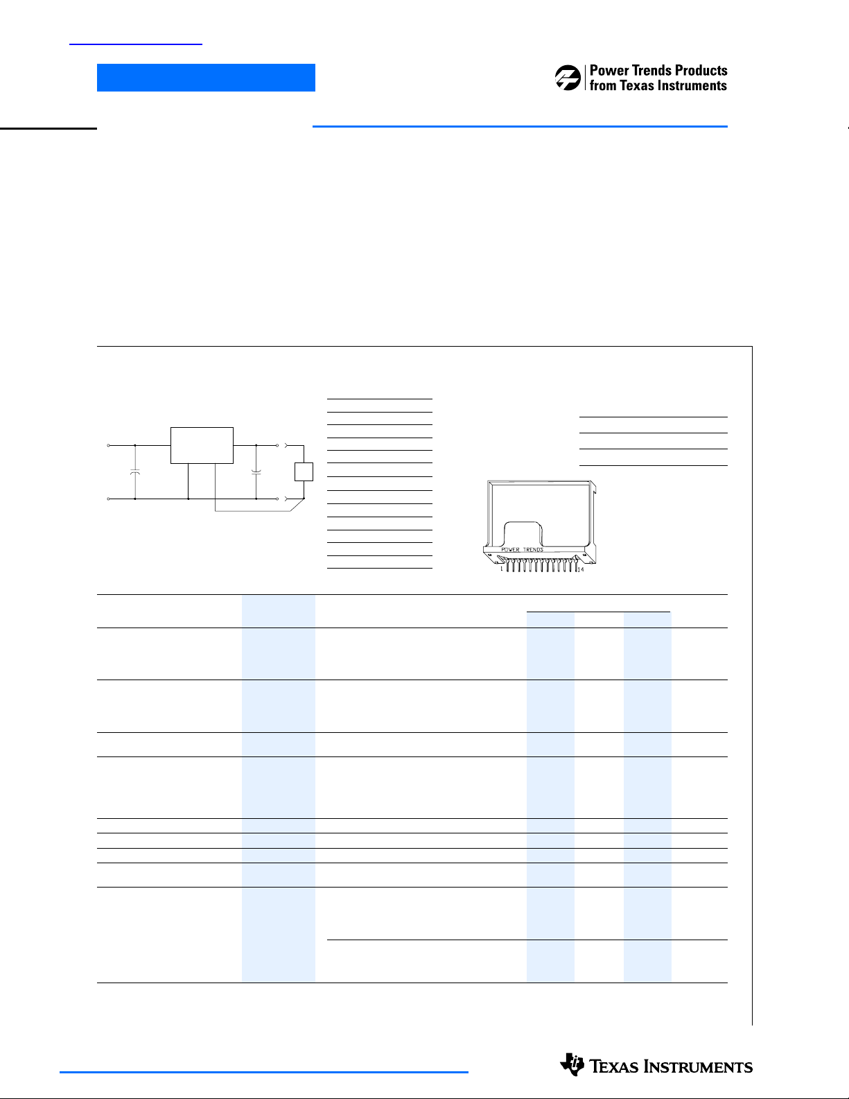
24W 12V Input Positive to Negative
Voltage Converter
Standard Application
V
COM
IN
4,5,6
+
C
1
C1 = Required 560µF electrolytic
C
= Required 330µF electrolytic
2
PT6640
11,12,13
1
7,8,9,10
C
2
REMOTE SENSE
SLTS037A
(Revised 6/30/2000)
• Wide Input Voltage Range:
+8V to +25V
• Negative Output:
–2.5V/4A to –15V/1.5A
• Adjustable Output Voltage
• 85% Efficiency
• Remote Sense Capability
Pin-Out Information
1 Remote Sense
2 Do Not Connect
3 Do Not Connect
4+V
-V
OUT
+
LOAD
COM
10 –V
11 GND
12 GND
13 GND
14 V
in
5+V
in
6+V
in
7 –V
out
8 –V
out
9 –V
out
out
Adjust
out
Ordering Information
PT6641 = –3.3 Volts
PT6642 = –5.0 Volts
PT6643 = –12.0 Volts
PT6644 = –9.0 Volts
PT6645 = –15.0 Volts
PT6646 = –2.5 Volts
PT6640
The PT6640 series is a positive
input to negative output line of
Integrated Switching Regulators
(ISRs). Designed for general purpose
applications, the PT6640 series delivers a negative output voltage at up
to 24W. The PT6640 is packaged in
a 14-Pin SIP (Single In-line Package)
and is available in a surface-mount
configuration.
Pkg Style 400
PT Series Suffix
Case/Pin Heat
Configuration Spreader
Vertical Through-Hole
Horizontal Through-Hole
Horizontal Surface Mount
Note: Back surface
of product is
conducting metal
(PT1234X)
P
D
E
Specifications
Characteristics
(Ta = 25°C unless noted) Symbols Conditions Min Typ Max Units
Output Current I
Input Voltage Range V
Output Voltage Tolerance ∆V
Output Voltage Adjust Range V
Line Regulation Reg
Load Regulation Reg
Vo Ripple/Noise V
Transient Response t
with C2 = 330µF V
o
in
o
oadj
line
load
n
tr
os
Efficiency η V
Ta = 60°C, 200 LFM, pkg P 0.1 — (See Note 2)
Ta = 25°C, natural convection V
0.1A ≤ Io ≤ I
Over V
Ta = -40°C to +65°C
max Vo = –2.5V/3.3V +8 — +27
o
range
in
Pin 14 to Vo or ground Vo = – 2.5V –1.8 — –4.3
+9V≤Vin≤+V
V
= +12V, 0.1≤ Io≤I
in
V
= +12V, Io = I
in
Io step between 0.5xIomax and Iomax — 200 — µSec
Vo over/undershoot — 100 — mV
= +12V, Io = 0.5x Iomax Vo = – 2.5V — 75 —
in
V
= +12V, Io = Iomax Vo = – 2.5V — 74 —
in
max, Io = Iomax — ±0.5 ±1.0 %V
in
max — ±0.5 ±1.0 %V
o
max — 3.0 — %V
o
Vo = –9.0/12.0/15.0V — 84 —
≤– 5.0V 0.1 — 4.0
o
V
= – 9.0V 0.1 — 2.5
o
V
= – 12.0V 0.1 — 2.0
o
Vo= – 15.0V 0.1 — 1.5
= – 5.0V +8 — +25
V
o
V
= – 9.0V +8 — +21 V
o
V
= – 12.0V +8 — +18
o
Vo = – 15.0V +8 — +15
= – 3.3V –2.2 — –4.7
V
o
V
= – 5.0V –3.0 — –6.5
o
= – 9.0V –6.0 — –10.2
V
o
V
= –12.0V –9.0 — –13.6
o
Vo = –15.0V –10.0 — –17.0
V
= – 3.3V — 79 —
o
= – 5.0V — 83 — %
V
o
V
= –9.0/12.0V — 85 —
o
Vo = –15.0V — 84 —
V
= – 3.3V — 77 —
o
V
= – 5.0V — 80 —
o
PT6640 SERIES
o-0.1 — Vo+0.1 V
V
Continued
A
V
o
o
o
%
For technical support and more information, see inside back cover or visit www.ti.com/powertrends
PT6640 Series
24W 12V Input Positive to Negative
Voltage Converter
Specifications
Characteristics
(Ta = 25°C unless noted) Symbols Conditions Min Typ Max Units
Switching Frequency ƒ
Absolute Maximum T
Operating Temperature Range
Storage Temperature T
(continued)
PT6640 SERIES
o
a
s
+9V ≤ V
Over Io range
Over V
— -40 — +125 °C
in
≤ V
in
range
in
max
500 550 600 kHz
-40 — +85
(2)
Mechanical Shock — Per Mil-STD-883D, Method 2002.3 — 500 — G’s
Mechanical Vibration — Per Mil-STD-883D, Method 2007.2,
20-2000 Hz, soldered in a PC board
— 7.5 — G’s
Weight — — — 14 — grams
Notes:
(1) The PT6640 Series requires a 330µF(output) and 560µF(input) electrolytic capacitors for proper operation in all applications.
(2) See Safe Operating Area curves or call the factory for guidance on thermal derating.
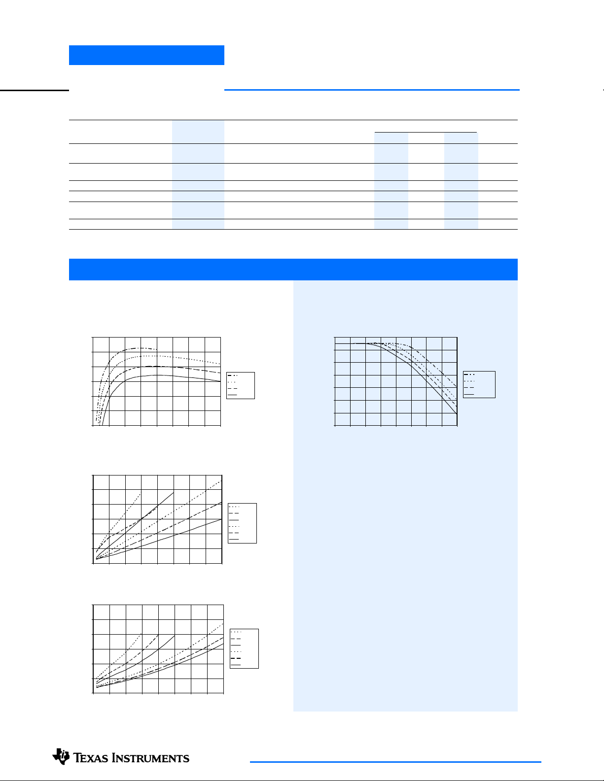
TYPICAL CHARACTERISTICS
Characteristic Curves @12.0V Vin (See Note A) Safe Operating Area Curves (See Note B)
Efficiency vs Output Current
90.0
85.0
80.0
75.0
Efficiency (%)
70.0
65.0
60.0
00.511.522.533.54
Output Current (A)
PT6643
PT6642
PT6641
PT6646
PT6642, @Vin =12V
90.0
80.0
70.0
60.0
50.0
40.0
Ambient Temperature ( C)
30.0
20.0
0.0 0.5 1.0 1.5 2.0 2.5 3.0 3.5 4.0
Output Current (A)
Airflow
200LFM
120LFM
60LFM
Nat conv
°C
Ripple vs Output Current
150
125
100
75
Ripple (mV)
50
25
0
00.511.522.533.54
Power Dissipation vs Output Current
6
5
4
3
PDiss (Watts)
2
1
0
00.511.522.533.54
Note A: Characteristic data has been developed from actual products tested at 25°C. This data is considered typical data for the DC-DC Converter.
Note B: SOA curves represent operating conditions at which internal components are at or below manufacturer’s maximum rated operating temperatures.
Output Current (A)
Output Current (A)
PT6645
PT6643
PT6644
PT6642
PT6641
PT6646
PT6645
PT6643
PT6644
PT6642
PT6641
PT6646
For technical support and more information, see inside back cover or visit www.ti.com/powertrends
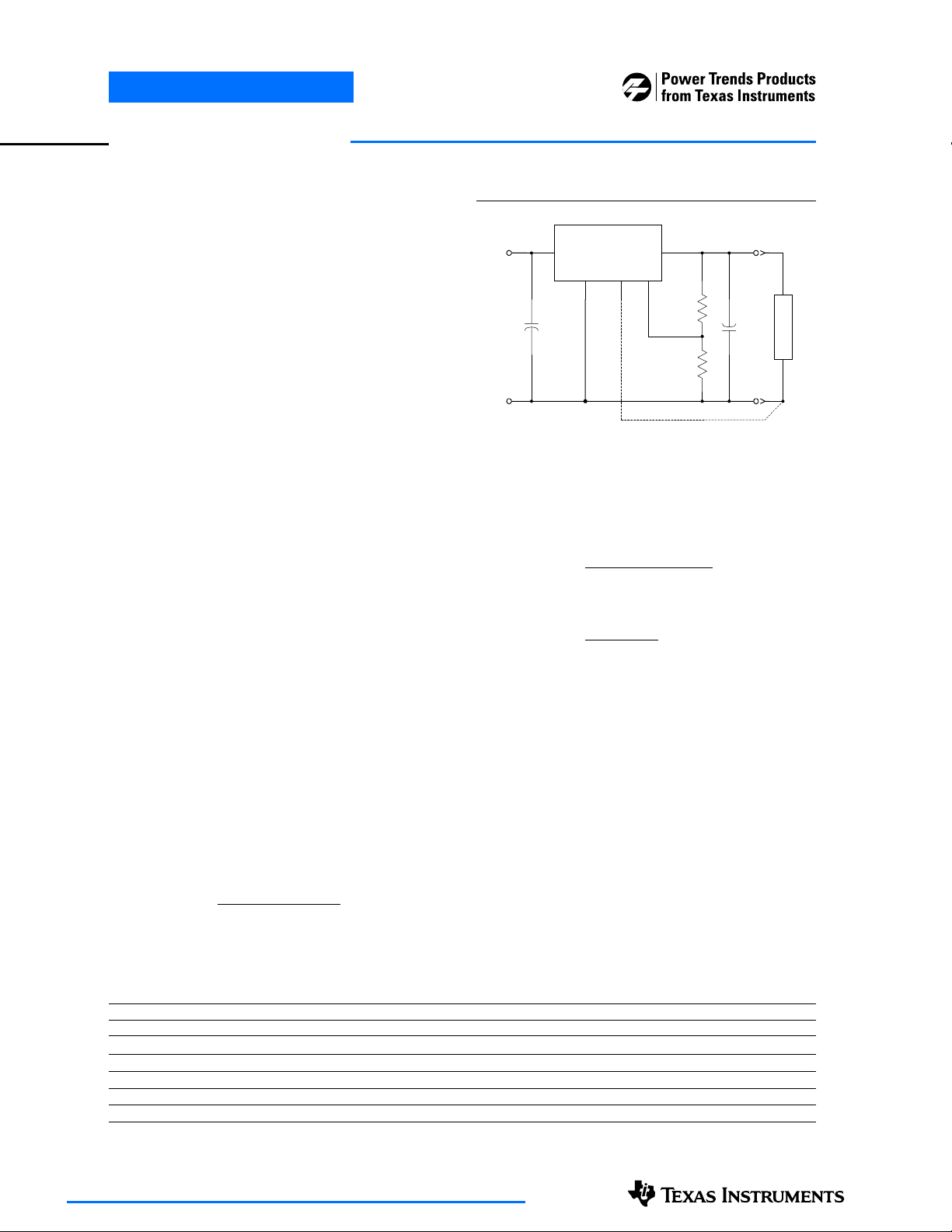
Application Notes
PT6640 Series
Adjusting the Output Voltage of the PT6640 24W
Positive to Negative ISR Series
The negative output voltage of the Power Trends
PT6640 series ISRs may be adjusted higher or lower than
the factory trimmed pre-set voltage with the addition of a
single external resistor. Table 1 gives the allowable adjustment range for each model in the series as V
and Va (max).
Adjust Up: An increase in the negative output
voltage is obtained by adding a resistor R2, between pin
adjust) and pins 7-10 (-V
14 (V
o
).
out
Adjust Down: Adding a resistor (R1), between pin 14
adjust) and pins 11-13 (GND), decreases the output
(V
o
voltage magnitude.
Refer to Figure 1 and Table 2 for both the placement and
value of the required resistor, either (R1) or R2 as appropriate.
Notes:
1. Use only a single 1% resistor in either the (R1) or R2
location. Place the resistor as close to the ISR as possible.
2. Never connect capacitors from V
, or the Remote Sense pin. Any capacitance added to
V
out
adjust pin will affect the stability of the ISR.
the V
3. If the Remote Sense feature is being used, connecting the
o
resistor (R1) between pin 14 (V
Sense) can benefit load regulation.
4. The maximum allowed input voltage (V
V
is adjusted. The difference between the input voltage
out
) and the output voltage (V
(V
in
10 × V
formulas to determine the maximum allowed input voltage
, whichever is less. Use one of the following
out
adjust to either GND,
o
adjust) and pin 1 (Remote
o
in
) must not exceed 30V or
out
for the PT6640.
V
greater than 2.73V,
out
(max) = 30 – V
V
in
For example, if V
V
(max) = 30 – -12 = 18Vdc
in
= -12V,
out
Vdc
out
(min)
a
) will change as
Figure 1
+V
in
C
in
560µF
4,5,6
+V in V out
PT6640
GND V
+
7,8,9,10
(adj)SNS(+)
o
1
1411,12,13
R2
| Up
|-V
(R1)
|-V
o
| Down
o
+
C
out
330µF
V
L
O
A
D
COMCOM
The values of (R1) [adjust down], and R2 [adjust up], can
also be calculated using the following formulas.
(R1) =
R2 =
Ro (Vo – 1.25)(Va – 1.25)
1.25 (V
Ro (Vo – 1.25)
- V
V
a
Where: Vo= Original V
= Adjusted V
V
a
= The resistance value in Table 1
R
o
= The series resistance from Table 1
R
s
– Va)
o
o
(magnitude)
out
(magnitude)
out
– R
– R
kΩ
s
s
kΩ
out
less than 2.73V,
V
out
(max) = 10 × V
V
in
Vdc
out
Table 1
PT6640 ADJUSTMENT AND FORMULA PARAMETERS
Series Pt # PT6646 PT6641 PT6642 PT6644 PT6643 PT6645
Vo (nom) –2.5V –3.3V –5.0V –9.0V –12.0V –15.0V
Va (min) –1.8V –2.2V –3.0V –6.0V –9.0V –10.0V
Va (max) –4.3V –4.7V –6.5V –10.2V –13.6V –17.0V
ΩΩ
Ro (k
Ω) 4.99 4.22 2.49 2.0 2.0 2.0
ΩΩ
ΩΩ
Rs (k
Ω) 2.49 4.99 4.99 12.7 12.7 12.7
ΩΩ
For technical support and more information, see inside back cover or visit www.ti.com/powertrends

Application Notes
continued
PT6640 Series
Table 2
PT6640 ADJUSTMENT RESISTOR VALUES
Series Pt # PT6646 PT6641 PT6642 Series Pt # PT6644 PT6643 PT6645
Current 4Adc 4Adc 4Adc Current 2.5Adc 2Adc 1.5Adc
Vo (nom) –2.5Vdc –3.3Vdc –5.0Vdc Vo (nom) –9.0Vdc –12.0Vdc –15.0Vdc
Va (req’d) Va (req’d)
–1.8 (1.4)kΩ –6.0 (6.9)kΩ
–1.9 (2.9)kΩ –6.2 (9.2)kΩ
–2.0 (5.0)kΩ –6.4 (11.9)kΩ
–2.1 (8.1)kΩ –6.6 (14.0)kΩ
–2.2 (13.3)kΩ (1.0)kΩ –6.8 (18.6)kΩ
–2.3 (23.7)kΩ (2.3)kΩ –7.0 (23.0)kΩ
–2.4 (54.9)kΩ (3.9)kΩ –7.2 (28.3)kΩ
–2.5 (5.8)kΩ –7.4 (35.0)kΩ
–2.6 59.9kΩ (8.4)kΩ –7.6 (43.5)kΩ
–2.7 28.7kΩ (11.7)kΩ –7.8 (55.0)kΩ
–2.8 18.3kΩ (16.5)kΩ –8.0 (71.0)kΩ
–2.9 13.1kΩ (23.6)kΩ –8.2 (95.0)kΩ
–3.0 10.0kΩ (35.4)kΩ (1.6)kΩ –8.4 (135.0)kΩ
–3.1 7.9kΩ (59.0)kΩ (2.3)kΩ –8.6 (215.0)kΩ
–3.2 6.4kΩ (130.0)kΩ (3.1)kΩ –8.8 (455.0)kΩ
–3.3 5.3kΩ (4.0)kΩ –9.0 (31.7)kΩ
–3.4 4.4kΩ 81.5kΩ (5.1)kΩ –9.2 64.8kΩ (36.1)kΩ
–3.5 3.8kΩ 38.3kΩ (6.2)kΩ –9.4 26.1kΩ (41.2)kΩ
–3.6 3.2kΩ 23.8kΩ (7.6)kΩ –9.6 13.1kΩ (47.1)kΩ
–3.7 2.7kΩ 16.6kΩ (9.1)kΩ –9.8 6.7kΩ (54.1)kΩ
–3.8 2.3kΩ 12.3kΩ (10.9)kΩ –10.0 2.8kΩ (62.6)kΩ (25.8)kΩ
–3.9 2.0kΩ 9.4kΩ (13.0)kΩ –10.2 0.2kΩ (72.8)kΩ (28.3)kΩ
–4.0 1.7kΩ 7.4kΩ (15.6)kΩ –10.4 (85.7)kΩ (31.1)kΩ
–4.1 1.4kΩ 5.8kΩ (18.7)kΩ –10.6 (102.0)kΩ (34.1)kΩ
–4.2 1.2kΩ 4.6kΩ (22.6)kΩ –10.8 (124.0)kΩ (37.3)kΩ
–4.3 1.0kΩ 3.7kΩ (27.6)kΩ –11.0 (155.0)kΩ (40.9)kΩ
–4.4 2.9kΩ (34.2)kΩ –11.2 (201.0)kΩ (44.9)kΩ
–4.5 2.2kΩ (43.6)kΩ –11.4 (278.0)kΩ (49.3)kΩ
–4.6 1.7kΩ (57.6)kΩ –11.6 (432.0)kΩ (54.3)kΩ
–4.7 1.2kΩ (80.9)kΩ –11.8 (895.0)kΩ (59.8)kΩ
–4.8 (128.0)kΩ –12.0 (66.1)kΩ
–4.9 (268.0)kΩ –12.2 94.8kΩ (73.3)kΩ
–5.0 –12.4 41.1kΩ (81.6)kΩ
–5.1 88.4kΩ –12.6 23.1kΩ (91.3)kΩ
–5.2 41.7kΩ –12.8 14.2kΩ (103.0)kΩ
–5.3 26.1kΩ –13.0 8.8kΩ (117.0)kΩ
–5.4 18.4kΩ –13.2 5.2kΩ (133.0)kΩ
–5.5 13.7kΩ –13.4 2.7kΩ (154.0)kΩ
–5.6 10.6kΩ –13.6 0.7kΩ (181.0)kΩ
–5.7 8.4kΩ –13.8 (217.0)kΩ
–5.8 6.7kΩ –14.0 (268.0)kΩ
–5.9 5.4kΩ –14.2 (343.0)kΩ
–6.0 4.4kΩ –14.5 (570.0)kΩ
–6.1 3.5kΩ –15.0
–6.2 2.8kΩ –15.5 42.3kΩ
–6.3 2.2kΩ –16.0 14.8kΩ
–6.4 1.7kΩ –16.5 5.6kΩ
–6.5 1.2kΩ –17.0 1.1kΩ
R1 = (Blue) R2 = Black
For technical support and more information, see inside back cover or visit www.ti.com/powertrends

I MPORTANT NOTI CE
T e xas Instrume nts and its subsidiarie s (TI) re se rve the right to make change s to the ir products or to discontinue
any product or se rvice without notice , and advise custome rs to obtain the late st ve rsion of re le vant information
to ve rify, be fore placing orde rs, that information be ing re lie d on is curre nt and comple te . All products are sold
subje ct to the te rms and conditions of sale supplie d at the time of orde r acknowle dgme nt, including those
pe rtaining to warranty, pate nt infringe me nt, and limitation of liability.
TI warrants pe rformance of its se miconductor products to the spe cifications applicable at the time of sale in
accordance with TI’s standard warranty. Te sting and othe r quality control te chnique s are utilize d to the e xte nt
TI de e ms ne ce ssary to support this warranty. Spe cific te sting of all parame te rs of e ach de vice is not ne ce ssarily
pe rforme d, e xce pt those mandate d by gove rnme nt re quire me nts.
Custome rs are re sponsible for the ir applications using TI compone nts.
In orde r to minimize risks associate d with the custome r’s applications, ade quate de sign and ope rating
safe guards must be provide d by the custome r to minimize inhe re nt or proce dural hazards.
TI assume s no liability for applications assistance or custome r product de sign. TI doe s not warrant or re pre se nt
that any lice nse , e ithe r e xpre ss or implie d, is grante d unde r any pate nt right, copyright, mask work right, or othe r
inte lle ctual prope rty right of TI cove ring or re lating to any combination, machine , or proce ss in which such
se miconductor products or se rvice s might be or are use d. TI’s publication of information re garding any third
party’s products or se rvice s doe s not constitute TI’s approval, warranty or e ndorse me nt the re of.
Copyright 2000, Te xas Instrume nts Incorporate d

PACKAGE OPTION ADDENDUM
www.ti.com
6-Feb-2006
PACKAGING INFORMATION
Orderable Device Status
PT6641D ACTIVE SIP MOD
PT6641E ACTIVE SIP MOD
PT6641P ACTIVE SIP MOD
PT6642D ACTIVE SIP MOD
PT6642E ACTIVE SIP MOD
PT6642G ACTIVE SIP MOD
PT6642P ACTIVE SIP MOD
PT6643D ACTIVE SIP MOD
PT6643E ACTIVE SIP MOD
PT6643L ACTIVE SIP MOD
PT6643M ACTIVE SIP MOD
PT6643P ACTIVE SIP MOD
PT6644D ACTIVE SIP MOD
PT6644E ACTIVE SIP MOD
PT6644P ACTIVE SIP MOD
PT6645D ACTIVE SIP MOD
PT6645E ACTIVE SIP MOD
PT6645F ACTIVE SIP MOD
PT6645G ACTIVE SIP MOD
PT6645P ACTIVE SIP MOD
PT6646E ACTIVE SIP MOD
PT6646P ACTIVE SIP MOD
(1)
The marketing status values are defined as follows:
ACTIVE: Product device recommended for new designs.
LIFEBUY: TI has announced that the device will be discontinued, and a lifetime-buy period is in effect.
NRND: Not recommended for new designs. Device is in production to support existing customers, but TI does not recommend using this part in
a new design.
PREVIEW: Device has been announced but is not in production. Samples may or may not be available.
(1)
Package
Type
ULE
ULE
ULE
ULE
ULE
ULE
ULE
ULE
ULE
ULE
ULE
ULE
ULE
ULE
ULE
ULE
ULE
ULE
ULE
ULE
ULE
ULE
Package
Drawing
EEA 14 12 TBD Call TI Level-1-215C-UNLIM
EEC 14 12 TBD Call TI Level-1-215C-UNLIM
EED 14 12 TBD Call TI Level-1-215C-UNLIM
EEA 14 12 Pb-Free
EEC 14 12 Pb-Free
EEG 14 12 Pb-Free
EED 14 12 Pb-Free
EEA 14 12 Pb-Free
EEC 14 12 Pb-Free
EEL 14 12 Pb-Free
EEM 14 12 Pb-Free
EED 14 12 Pb-Free
EEA 14 12 Pb-Free
EEC 14 12 Pb-Free
EED 14 12 Pb-Free
EEA 14 12 Pb-Free
EEC 14 12 Pb-Free
EEF 14 12 Pb-Free
EEG 14 12 Pb-Free
EED 14 12 Pb-Free
EEC 14 12 Pb-Free
EED 14 12 Pb-Free
Pins Package
Qty
Eco Plan
(RoHS)
(RoHS)
(RoHS)
(RoHS)
(RoHS)
(RoHS)
(RoHS)
(RoHS)
(RoHS)
(RoHS)
(RoHS)
(RoHS)
(RoHS)
(RoHS)
(RoHS)
(RoHS)
(RoHS)
(RoHS)
(RoHS)
(2)
Lead/Ball Finish MSL Peak Temp
Call TI N / A for Pkg Type
Call TI Level-1-215C-UNLIM
Call TI N / A for Pkg Type
Call TI N / A for Pkg Type
Call TI N / A for Pkg Type
Call TI Level-1-215C-UNLIM
Call TI Level-1-215C-UNLIM
Call TI N / A for Pkg Type
Call TI N / A for Pkg Type
Call TI N / A for Pkg Type
Call TI Level-1-215C-UNLIM
Call TI N / A for Pkg Type
Call TI N / A for Pkg Type
Call TI Level-1-215C-UNLIM
Call TI Level-1-215C-UNLIM
Call TI N / A for Pkg Type
Call TI N / A for Pkg Type
Call TI Level-1-215C-UNLIM
Call TI N / A for Pkg Type
(3)
Addendum-Page 1

PACKAGE OPTION ADDENDUM
www.ti.com
OBSOLETE: TI has discontinued the production of the device.
(2)
Eco Plan - The planned eco-friendly classification: Pb-Free (RoHS), Pb-Free (RoHS Exempt), or Green (RoHS & no Sb/Br) - please check
http://www.ti.com/productcontent for the latest availability information and additional product content details.
TBD: The Pb-Free/Green conversion plan has not been defined.
Pb-Free (RoHS): TI's terms "Lead-Free" or "Pb-Free" mean semiconductor products that are compatible with the current RoHS requirements
for all 6 substances, including the requirement that lead not exceed 0.1% by weight in homogeneous materials. Where designed to be soldered
at high temperatures, TI Pb-Free products are suitable for use in specified lead-free processes.
Pb-Free (RoHS Exempt): This component has a RoHS exemption for either 1) lead-based flip-chip solder bumps used between the die and
package, or 2) lead-based die adhesive used between the die and leadframe. The component is otherwise considered Pb-Free (RoHS
compatible) as defined above.
Green (RoHS & no Sb/Br): TI defines "Green" to mean Pb-Free (RoHS compatible), and free of Bromine (Br) and Antimony (Sb) based flame
retardants (Br or Sb do not exceed 0.1% by weight in homogeneous material)
(3)
MSL, Peak Temp. -- The Moisture Sensitivity Level rating according to the JEDEC industry standard classifications, and peak solder
temperature.
Important Information and Disclaimer:The information provided on this page represents TI's knowledge and belief as of the date that it is
provided. TI bases its knowledge and belief on information provided by third parties, and makes no representation or warranty as to the
accuracy of such information. Efforts are underway to better integrate information from third parties. TI has taken and continues to take
reasonable steps to provide representative and accurate information but may not have conducted destructive testing or chemical analysis on
incoming materials and chemicals. TI and TI suppliers consider certain information to be proprietary, and thus CAS numbers and other limited
information may not be available for release.
In no event shall TI's liability arising out of such information exceed the total purchase price of the TI part(s) at issue in this document sold by TI
to Customer on an annual basis.
6-Feb-2006
Addendum-Page 2

IMPORTANT NOTICE
Texas Instruments Incorporated and its subsidiaries (TI) reserve the right to make corrections, modifications,
enhancements, improvements, and other changes to its products and services at any time and to discontinue
any product or service without notice. Customers should obtain the latest relevant information before placing
orders and should verify that such information is current and complete. All products are sold subject to TI’s terms
and conditions of sale supplied at the time of order acknowledgment.
TI warrants performance of its hardware products to the specifications applicable at the time of sale in
accordance with TI’s standard warranty. Testing and other quality control techniques are used to the extent TI
deems necessary to support this warranty. Except where mandated by government requirements, testing of all
parameters of each product is not necessarily performed.
TI assumes no liability for applications assistance or customer product design. Customers are responsible for
their products and applications using TI components. To minimize the risks associated with customer products
and applications, customers should provide adequate design and operating safeguards.
TI does not warrant or represent that any license, either express or implied, is granted under any TI patent right,
copyright, mask work right, or other TI intellectual property right relating to any combination, machine, or process
in which TI products or services are used. Information published by TI regarding third-party products or services
does not constitute a license from TI to use such products or services or a warranty or endorsement thereof.
Use of such information may require a license from a third party under the patents or other intellectual property
of the third party, or a license from TI under the patents or other intellectual property of TI.
Reproduction of information in TI data books or data sheets is permissible only if reproduction is without
alteration and is accompanied by all associated warranties, conditions, limitations, and notices. Reproduction
of this information with alteration is an unfair and deceptive business practice. TI is not responsible or liable for
such altered documentation.
Resale of TI products or services with statements different from or beyond the parameters stated by TI for that
product or service voids all express and any implied warranties for the associated TI product or service and
is an unfair and deceptive business practice. TI is not responsible or liable for any such statements.
Following are URLs where you can obtain information on other Texas Instruments products and application
solutions:
Products Applications
Amplifiers amplifier.ti.com Audio www.ti.com/audio
Data Converters dataconverter.ti.com Automotive www.ti.com/automotive
DSP dsp.ti.com Broadband www.ti.com/broadband
Interface interface.ti.com Digital Control www.ti.com/digitalcontrol
Logic logic.ti.com Military www.ti.com/military
Power Mgmt power.ti.com Optical Networking www.ti.com/opticalnetwork
Microcontrollers microcontroller.ti.com Security www.ti.com/security
Telephony www.ti.com/telephony
Video & Imaging www.ti.com/video
Wireless www.ti.com/wireless
Mailing Address: Texas Instruments
Post Office Box 655303 Dallas, Texas 75265
Copyright 2006, Texas Instruments Incorporated
 Loading...