

查询PT4560供应商
PT4560 Series
30-W 48-V Input
Isolated DC/DC Converter
Description
The PT4560 series is a single-output
isolated DC/DC converter, housed in a
19-pin space-saving package. These modules are UL, CSA, and VDE approved
for telecom applications, and rated at
30 watts or 8 A. Standard output voltages
range from 1.8 V to 15 V, each adjustable
by up to ±10% of nominal.
Operating features include a remote
on/off control, an under-voltage-lockout
(UVLO), and a differential remote sense.
The PT4560 series also incorporates
many protection features. These include
output current limit, short-circuit protection, and over-temperature shutdown.
PT4560 requires a 330µF of output
capacitance for proper operation.
Features
• Input Voltage Range:
36V to 75V
• 1500 VDC Isolation
• On/Off Control
Adjust
• V
o
• Differential Remote Sense
• Current Limit
• Short-Circuit Protection
• Over-Temperature Shutdown
Ordering Information
PT4561H = 3.3V/8A (26.4W)
PT4562H = 5.0V/6A
PT4563H = 12.0V/2.5A
PT4564H = 15.0V/2A
PT4565H = 2.0V/8A (16W)
PT4566H = 2.5V/8A (20W)
PT4567H = 1.8V/8A (14.4W)
PT4568H = 5.2V/6A
PT4571H = 9.0V/3.3A
PT Series Suffix
Case/Pin Order Package
Configuration Suffix Code *
Vertical N (END)
Horizontal A (ENA)
SMD C (ENC)
* Previously known as package styles 1400 &
1410.
(Reference the applicable package code drawing for the dimensions and PC board layout)
(PT1234x )
(Revised 3/14/2002)
• Undervoltage Lockout
• Space-Saving Package
• Solderable Copper Case
• UL1950 Recognized
• CSA 22.2 950 Certified
• EN60950 Approved
• VDE Licensed
• 4.9 x10
6
Hrs MTBF
• Meets FCC Class A
Radiated Limits
Pin-Out Information
Pin Function
1 Do Not Use
2 Remote On/Off †
3 Do Not Use
4-V
in
5-V
in
6-V
in
7+V
in
8+V
in
9+V
in
10 -V
o
11 -V
o
12 -V
o
13 -Remote Sense
14 +V
o
15 +V
o
16 +V
o
17 +V
o
18 Vo Adjust †
19 +Remote Sense
†For more information,
see application notes.
SLTS097C
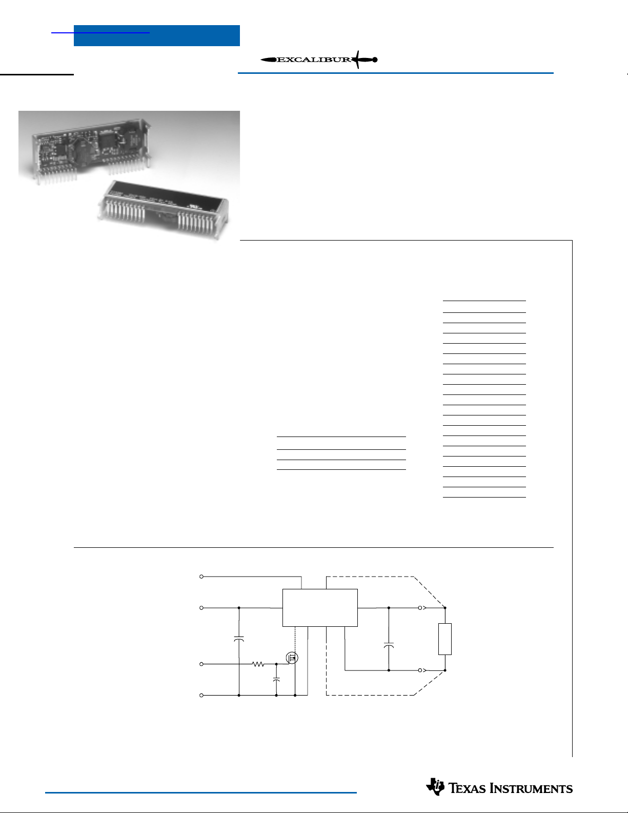
Standard Application
For technical support and more information, see inside back cover or visit www.ti.com
VO Adjust
+V
IN
Inhibit
–V
IN
+REMOTE SENSE
19
18
+V
7, 8, 9 14-17
+
C
IN
R
1
C
1
Q
1
PT4560
4-6 10-1213
2
+
C
OUT
–REMOTE SENSE
O
L
O
A
D
–V
O
Cin= Optional 100µF/100V electrolytic
C
= Required 330µF electrolytic (See Notes)
out
Q1= N-Channel MOSFET
R1/C1= Optional (see application notes)

PT4560 Series
30-W 48-V Input
Isolated DC/DC Converter
Specifications (Unless otherwise stated, T
=25°C, Vin =48V, C
a
=330µF, and Io =Iomax)
out
PT4560 SERIES
Characteristic Symbol Conditions Min Typ Max Units
Output Current I
Input Voltage Range V
o
in
Over Vin range Vo = 15 V 0.1
Over Io Range 36.0 48.0 75.0 V
Set Point Voltage Tolerance Vo tol V
Temperature Variation Reg
Line Regulation Reg
Load Regulation Reg
Total Output Voltage Variation ∆V
temp
line
load
tot Includes set-point, line, load, V
o
–40° ≤Ta ≤ +85°C — ±0.5 — %V
Over Vin range V
Over I
range Vo ≥5.0V — ±0.4 ±1.0 %V
o
= 12 V 0.1
V
o
V
= 9.0V 0.1
o
=5.0V 0.25
V
o
V
≤ 3.3V 0.25
o
≥5.0V — ±1 ±1.5 %V
o
V
≤3.3V — ±33 ±50 mV
o
≥5.0V — ±0.2 ±1.0 %V
o
V
≤3.3V — ±7 ±33 mV
o
V
≤3.3V — ±13 ±33 mV
o
≥5.0V — ±2 — %V
o
(1)
(1)
(1)
(1)
(1)
— 2.0
— 2.5
— 3.3
— 6.0
— 8.0
–40° ≤Ta ≤ +85°C Vo ≤3.3V — ±67 — mV
Efficiency η V
Vo Ripple (pk-pk) V
Transient Response t
Short Circuit Current I
Switching Frequency ƒ
∆V
r
tr
tr
sc
s
Under-Voltage Lockout UVLO V
Remote On/Off Input (pin 2) Referenced to –Vin (pins 4–6)
Input High Voltage V
Input Low Voltage V
Input Low Current I
IH
IL
IL –3 –6 –10 µA
20MHz bandwidth V
0.1A/µs load step, 50% to 100% Iomax — 100 200 µs
Vo over/undershoot V
Over Vin range V
increasing — 34 —
in
Vin decreasing — 33 —
= 1 5V — 85 —
o
= 1 2V — 87 —
V
o
=9.0V — 84 —
V
o
=5.0V — 84 —
V
o
=3.3V — 80 —
V
o
Vo =1.8V — 69 —
≥ 5.0V — 1.0 2.0 %V
o
V
≤ 3.3V — 50 75 mV
o
≥ 5.0V — ±3.0 ±5.0 %V
o
V
≤ 3.3V — ±100 ±150 mV
o
— 2xIomax — A
≥10V 400 500 600
o
V
<10V 600 750 900
o
2.5 — 15
–0.2 — +0.8
(2)
Standby Input Current Iin standby pins 2 & 4 connected — 8 16 mA
Internal Input Capacitance C
External Output Capacitance C
Isolation Voltage Input-output/input-case 1500 — — Vdc
Capacitance Input-output — 1200 — pF
Resistance Input-output 10 — — MΩ
Operating Temperature Range T
Maximum Case Temperature T
Storage Temperature Range T
Reliability MTBF Per Bellcore TR-332
Mechanical Shock — Per Mil-Std-883D, method 2002.3,
Mechanical Vibration — Per Mil-Std-883D, method 2007.2,
in
out
a
c
s
Between +Vo and –V
o
V
≥ 9.0V 260 330 600
o
V
≤ 5.0V 260 330 1,000
o
Over Vin range -40
50% stress, Ta =40°C, ground benign
1mS, half-sine, mounted to a fixture
20-2000Hz, soldered in board
— 0.66 — µF
(3)
(3)
(4)
— +85
(5)
— — 100 °C
-40 — +125 °C
4.9 — — 10
— 500 — G’s
—20—G’s
Weight — — — 40 — grams
Flammability — Materials meet UL 94V-0
Notes: (1) The DC/DC converter will operate at no load with reduced specifications.
(2) The Remote On/Off input has an internal pull-up. If it is left open circuit the PT4560 will operate when input power is applied. A low-leakage
(<100nA) MOSFET is recommended to control this input. The open-circuit voltage is less than 10V. See application notes for interface considerations.
(3) Output capacitor values are absolute. Allowances must be made for any additional de-coupling capacitors and the total external capacitor tolerance.
The value of external capacitance is limited due to regulator startup current requirements. Consult the factory for further details.
(4) For operation below 0°C, the required external output capacitor must have temperature stable characteristics. E.g. Tantalum or Oscon® types.
(5) See Safe Operating Area curves or contact the factory for the appropriate thermal derating.
A
%
kHz
V
V
µF
°C
6
o
o
o
o
o
o
pp
o
Hrs
For technical support and more information, see inside back cover or visit www.ti.com
PT4560 Series
30-W 48-V Input
Isolated DC/DC Converter
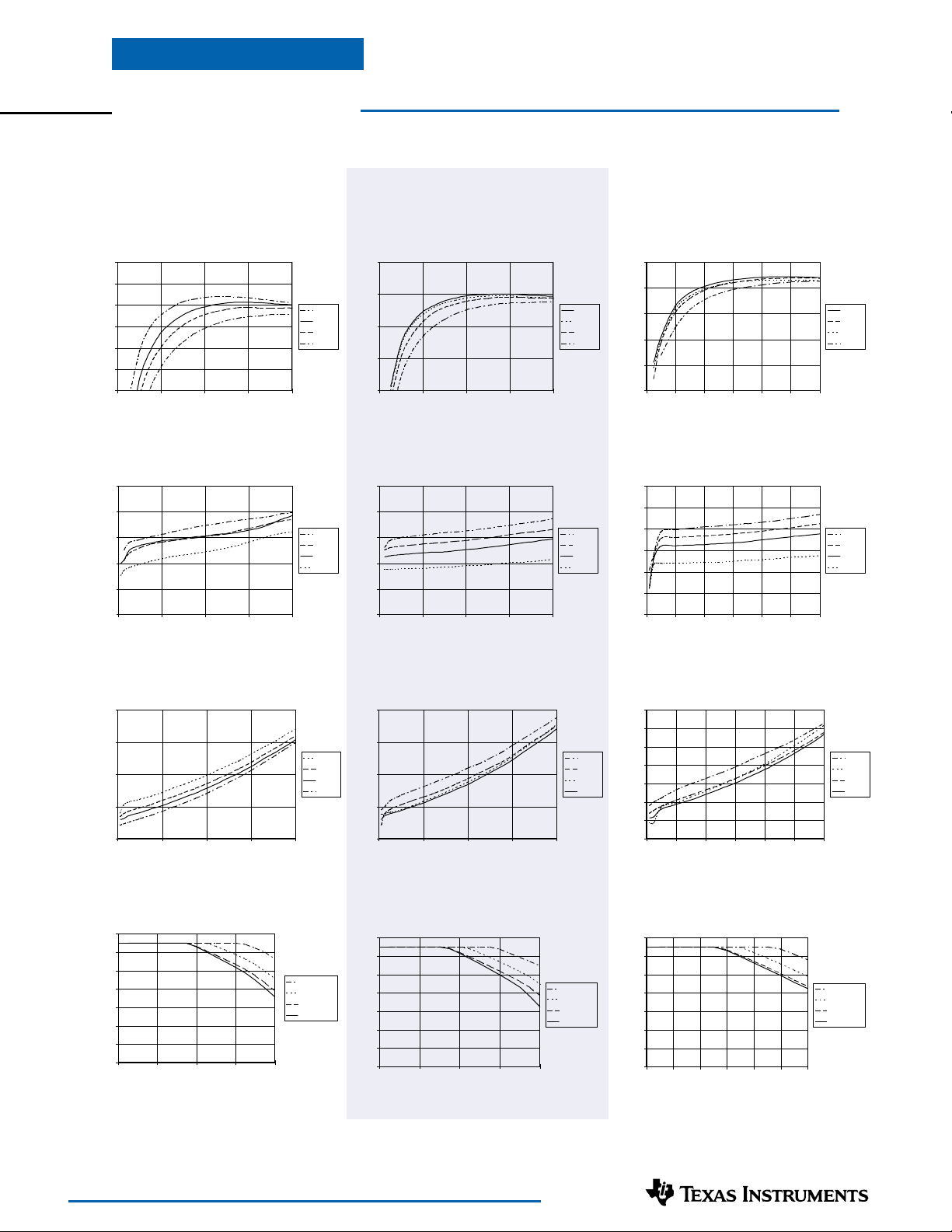
T ypical Characteristics
PT4567, 1.8 VDC (See Note A)
Efficiency vs Output Current
80
75
70
65
60
Efficiency - %
55
50
02468
Ripple vs Output Current
20
16
12
8
Ripple - mV
4
0
02468
Iout (A)
Iout (A)
V
IN
36.0V
48.0V
60.0V
75.0V
V
IN
75.0V
60.0V
48.0V
36.0V
PT4561, 3.3 VDC (See Note A)
Efficiency vs Output Current
90
80
70
Efficiency - %
60
50
02468
Ripple vs Output Current
50
40
30
20
Ripple - mV
10
0
02468
Iout (A)
Iout (A)
V
IN
48.0V
36.0V
60.0V
75.0V
V
IN
75.0V
60.0V
48.0V
36.0V
PT4562, 5.0 VDC (See Note A)
Efficiency vs Output Current
90
80
70
60
Efficiency - %
50
40
0123456
Ripple vs Output Current
60
50
40
30
Ripple - mV
20
10
0
0123456
Iout (A)
Iout (A)
V
IN
48.0V
60.0V
36.0V
75.0V
V
IN
75.0V
60.0V
48.0V
36.0V
Power Dissipation vs Output Current
8
6
4
Pd - Watts
2
0
02468
Safe Operating Area, Vin =48V (See Note B)
90
80
70
60
50
40
30
Ambient Temperature (°C)
20
0.0 2.0 4.0 6.0 8.0
Note A: All data listed in the above graphs has been developed from actual products tested at 25°C. This data is considered typical data for the DC-DC Converter.
Note B: SOA curves represent operating conditions at which internal components are at or below manufacturer’s maximum rated operating temperature.
Iout (A)
Iout (A)
V
Airflow
200LFM
120LFM
60LFM
Nat Conv
IN
75.0V
60.0V
48.0V
36.0V
Power Dissipation vs Output Current
8
6
4
Pd - Watts
2
0
02468
Safe Operating Area, Vin =48V (See Note B)
90
80
70
60
50
40
30
Ambient Temperature (°C)
20
02468
Iout (A)
Iout (A)
Airflow
200LFM
120LFM
60LFM
Nat conv
V
IN
75.0V
60.0V
36.0V
48.0V
Power Dissipation vs Output Current
7
6
5
4
3
Pd - Watts
2
1
0
0123456
Safe Operating Area, Vin =48V (See Note B)
90
80
70
60
50
40
30
Ambient Temperature (°C)
20
0123456
Iout (A)
Iout (A)
Airflow
200LFM
120LFM
60LFM
Nat conv
V
IN
75.0V
36.0V
60.0V
48.0V
For technical support and more information, see inside back cover or visit www.ti.com

PT4560 Series
30-W 48-V Input
Isolated DC/DC Converter
T ypical Characteristics
PT4571, 9.0 VDC (See Note A)
Efficiency vs Output Current
90
85
80
75
70
Efficiency - %
65
60
00.511.522.53
Ripple vs Output Current
150
120
90
60
Ripple - mV
30
0
00.511.522.53
Iout (A)
Iout (A)
V
V
IN
75.0V
60.0V
48.0V
36.0V
IN
36.0V
48.0V
60.0V
75.0V
PT4563, 12.0 VDC (See Note A)
Efficiency vs Output Current
90
85
80
75
70
65
Efficiency - %
60
55
50
00.511.522.5
Ripple vs Output Current
200
160
120
80
Ripple - mV
40
0
00.511.522.5
Iout (A)
Iout (A)
V
75.0V
60.0V
48.0V
36.0V
V
IN
IN
36.0V
48.0V
60.0V
75.0V
PT4564, 15 VDC (See Note A)
Efficiency vs Output Current
90
80
70
Efficiency - %
60
50
00.511.52
Ripple vs Output Current
400
300
200
Ripple - mV
100
0
00.511.52
Iout (A)
Iout (A)
V
IN
48.0V
60.0V
75.0V
36.0V
V
IN
75.0V
60.0V
48.0V
36.0V
Power Dissipation vs Output Current
7
6
5
4
3
Pd - Watts
2
1
0
0 0.5 1 1.5 2 2.5 3
Safe Operating Area, Vin =48V (See Note B)
90
80
70
60
50
40
30
Ambient Temperature (°C)
20
0.0 0.5 1.0 1.5 2.0 2.5 3.0
Note A: All data listed in the above graphs has been developed from actual products tested at 25°C. This data is considered typical data for the DC-DC Converter.
Note B: SOA curves represent operating conditions at which internal components are at or below manufacturer’s maximum rated operating temperature.
Iout (A)
Iout (A)
V
Airflow
200LFM
120LFM
60LFM
Nat Conv
IN
75.0V
60.0V
48.0V
36.0V
Power Dissipation vs Output Current
6
5
4
3
Pd - Watts
2
1
0
0 0.5 1 1.5 2 2.5
Safe Operating Area, Vin =48V (See Note B)
90
80
70
60
50
40
30
Ambient Temperature (°C)
20
00.511.522.5
Iout (A)
Iout (A)
V
75.0V
60.0V
48.0V
36.0V
Airflow
200LFM
120LFM
60LFM
Nat conv
IN
Power Dissipation vs Output Current
8
6
4
Pd - Watts
2
0
0 0.5 1 1.5 2
Safe Operating Area, V
90
80
70
60
50
40
30
Ambient Temperature (°C)
20
0.0 0.5 1.0 1.5 2.0
Iout (A)
Iout (A)
=48V (See Note B)
in
Airflow
200LFM
120LFM
60LFM
Nat Conv
V
IN
36.0V
75.0V
60.0V
48.0V
For technical support and more information, see inside back cover or visit www.ti.com

Application Notes
j)
)
)
PT3320/3340/4560/4580 Series
Adjusting the Output Voltage of Power Trends’
30W Isolated DC/DC Converter Series
The factory pre-set output voltage of Power Trends’ 30W
series of isolated DC/DC converters may be adjusted
within a nominal ±10% range. This is accomplished with
the addition of a single external resistor. For the input
voltage range specified in the data sheet, Table 1 gives the
allowable adjustment range for each model as Vo (min)
and Vo (max).
Adjust Up: An increase in the output voltage is obtained
by adding a resistor, R
between Vo adjust (pin 18), and
2
-Remote Sense (pin 13). See note 4.
Adjust Down: Add a resistor (R
), between Vo adjust (pin
1
18), and +Remote Sense (pin 19).
3. If the remote sense pins are not being used, the resistors
(R1) and R2 can be connected to +V
out
or -V
out
respectively.
4. The adjusted output voltage, V
effectively sets the voltage
a
across pins 13 and 19 (±Remote Sense). When using the
remote sense pins, V
(measured directly across pins 10–
out
12, and 14–17) can be significantly higher than V
exceed Vo (max). If Va is adjusted upward of Vo(max), the
the minimum input voltage is increased by the same
percentage as V
exceeds Vo(max).
out
The values of (R1) [adjust down], and R2 [adjust up], can
also be calculated using the following formulas.
K
(Va – Vr)
(R1) =
o
Vr (Vo – Va)
– R
s
Refer to Figure 1 and Tables 2 & 3 for both the placement and
value of the required resistor, (R
Notes:
1. Use only a single 1% resistor in either the (R1) or R
location. Place the resistor as close to the ISR as possible.
2. Never connect capacitors to V
added to the V
adjust control pin will affect the stability of
o
the ISR.
Table 1
DC/DC CONVERTER ADJUSTMENT RANGE AND FORMULA PARAMETERS
Series Pt #
AL Case:
24V Bus PT3341 PT3342 PT3343 PT3344
48V Bus PT3327 PT3325 PT3326 PT3321 PT3322 PT3323 PT3324
CU Case:
24V Bus PT4585 PT4581 PT4582 PT4583 PT4584
48V Bus PT4567 PT4565 PT4566 PT4561 PT4562 PT4571 PT4563 PT4564
Vo(nom) 1.8V 1.8V 2.0V 2.5V 3.3V 5.0V 9.0V 12.0V 15.0V
Vo(min) 1.62V 1.62V 1.8V 2.25V 2.95V 4.5V 7.0V 10.8V 13.5V
Vo(max) 2.5V 1.98V 2.2V 2.75V 3.65V 5.5V 10.0V 13.2V 16.5V
V
r
ΩΩ
Ko (V·k
Ω) 69.58 69.58 62.47 42.33 68.89 68.71 133.25 135.9 137.5
ΩΩ
ΩΩ
Rs (k
Ω) 80.6 80.6 150.0 121.0 150.0 121.0 110 90.9 80.6
ΩΩ
1.225V 1.225V 1.225V 1.225V 1.225V 1.225V 2.5V 2.5V 2.5V
) or R2.
1
adjust. Any capacitance
o
K
R
2
2
Where V
=
o
V
a
V
r
K
o
R
s
(V
o
– Vo)
a
– R
s
= Original output voltage
= Adjusted output voltage
= Reference voltage (Table 1)
= Multiplier constant (Table 1)
= Series resistance (Table 1)
, and may
a
kΩ
kΩ
Figure 1
2
Remote
On/Off
7, 8, 9
+V
in
Cin
µ
100
F
100V
(Optional)
-V
in
For technical support and more information, see inside back cover or visit www.ti.com
+Vin +Vout
30W Isolated
-Vin Vo(ad
-Vout
10 - 12
+
Sns(-
13
19
Sns(+
184, 5, 6
(R1)
Adj Down
14 - 17
R2
Adj
Up
Cout
330
+V
out
L
O
+
µ
F
A
D
-V
out

Application Notes
continued
PT3320/3340/4560/4580 Series
Table 2
DC/DC CONVERTER ADJUSTMENT RESISTOR VALUES
Series Pt #
AL Case
24V Bus PT3341
48V Bus PT3327 PT3325 PT3326 PT3321
CU Case
24V Bus PT4585 PT4581
48V Bus PT4567 PT4565 PT4566 PT4561
Current 8Adc 8Adc 8Adc 8Adc 8Adc
Vo(nom) 1.8V 1.8V 2.0V 2.5V 3.3V
Va(req’d)
1.65 (80.3)kΩ (80.3)kΩ
1.7 (189.0)kΩ (189.0)kΩ
1.75 (516.0)kΩ (516.0)kΩ
1.8
1.85 1.31MΩ 1.31MΩ (62.5)kΩ
1.9 615.0kΩ 615.0kΩ (194.0)kΩ
1.95 383.0kΩ 383.0kΩ (589.0)kΩ
2.0 267.0kΩ
2.05 198.0kΩ 1.1MΩ
2.1 151.0kΩ 475.0kΩ
2.15 118.0kΩ 266.0kΩ
2.2 93.3kΩ 162.0kΩ
2.25 74.0kΩ (20.7)kΩ
2.3 58.6kΩ (64.7.0)kΩ
2.35 45.9kΩ (138.0)kΩ
2.4 35.4kΩ (285.0)kΩ
2.45 26.4kΩ (726.0)kΩ
2.5 18.8kΩ
2.55 726.0kΩ
2.6 302.0kΩ
2.65 161.0kΩ
2.7 90.6kΩ
2.75 48.3kΩ
2.95 (127.0)kΩ
3.0 (183.0)kΩ
3.05 (261.0)kΩ
3.1 (377.0)kΩ
3.15 (572.0)kΩ
3.2 (961.0)kΩ
3.25 (2.13)MΩ
3.3
3.35 1.23MΩ
3.4 539.0kΩ
3.45 309.0kΩ
3.5 194.0kΩ
3.55 126.0kΩ
3.6 79.6kΩ
3.65 46.8kΩ
R1 = (Blue) R2 = Black
For technical support and more information, see inside back cover or visit www.ti.com

Application Notes
PT3320/3340/4560/4580 Series
Table 3
DC/DC CONVERTER ADJUSTMENT RESISTOR VALUES
Series Pt #
AL Case
24V Bus PT3342 PT3343 PT3344
48V Bus PT3322 PT3323 PT3324
CU Case
24V Bus PT4582 PT4583 PT4584
48V Bus PT4562 PT4571 PT4563 PT4564
Current 6Adc 3.3Adc 2.5Adc 2.0Adc
Vo(nom) 5.0V 9.0V 12.0V 15.0V
Va(req’d) Va(req’d)
4.5 (246.0)kΩ 7.0 (9.9)kΩ
4.55 (293.0)kΩ 7.2 (29.2)kΩ
4.6 (352.0)kΩ 7.4 (53.2)kΩ
4.65 (428.0)kΩ 7.6 (84.2)kΩ
4.7 (529.0)kΩ 7.8 (125.0)kΩ
4.75 (670.0)kΩ 8.0 (183.0)kΩ
4.8 (882.0)kΩ 8.2 (270.0)kΩ
4.85 (1.23)MΩ 8.4 (414.0)kΩ
4.9 (1.94)MΩ 8.6 (703.0)kΩ
4.95 8.8 (1.57)MΩ
5.0 9.0
5.05 9.2 556.0kΩ
5.1 566.0kΩ 9.4 223.0kΩ
5.15 337.0kΩ 9.6 112.0kΩ
5.2 223.0kΩ 9.8 56.6kΩ
5.25 154.0kΩ 10.0 23.3kΩ
5.3 108.0kΩ •
5.35 75.3kΩ 10.8 (285.0)kΩ
5.4 50.8kΩ 11.0 (371.0)kΩ
5.45 31.7kΩ 11.2 (500.0)kΩ
5.5 16.4kΩ 11.4 (715.0)kΩ
11.6 (1.15)MΩ
11.8
12.0
12.2 588.0kΩ
12.4 249.0kΩ
12.6 136.0kΩ
12.8 78.9kΩ
13.0 45.0kΩ
13.2 22.3kΩ
•
13.5 (323.0)kΩ
13.6 (355.0)kΩ
13.8 (437.0)kΩ
14.0 (522.0)kΩ
14.2 (724.0)kΩ
14.4 (1010.0)kΩ
14.6 (1.58)MΩ
14.8
15.0
15.2 607.0kΩ
15.4 263.0kΩ
15.6 149.0kΩ
15.8 91.3kΩ
16.0 56.9kΩ
16.5 11.1kΩ
R1 = (Blue) R2 = Black
For technical support and more information, see inside back cover or visit www.ti.com
Application Notes
PT3320/3340/4560/4580 Series
Using Remote On/Off on Power Trends’
30W Isolated DC-DC Converter Series
Power Trends’ 30W isolated series of DC/DC converters
incorporate a Remote On/Off function. This function may
be used in applications for battery conservation, powerup/shutdown sequencing, or to co-ordinate the power-up
of the regulator for active in-rush current control. (See
TI application reports, SLTA021, and SLUA250).
The Remote On/Off function is provided by pin 2. If
pin 2 is left open-circuit, the converter provides a regulated output whenever a valid source voltage
between +V
(pins 7-9), and –Vin (pins 4-6). Applying
in
1
is applied
a low voltage 2, with respect to –Vin (pin 2), disables the
regulator output 3. Table 1 details the control requirements
for this input. Figure 1 shows how a discrete MOSFET
(Q1) may be referenced to the negative input voltage rail
to control the Remote On/Off pin.
Table 1 Remote On/Off Control Requirements
Parameter min max
Enable (VIH) 2.5V
Disable (VIL) –0.3V 0.8V
5
15V (or open circuit)
2
4
Notes:
1. These converters incorporate an “Under Voltage Lockout”
(UVLO) function. This function automatically holds the
converter output in the “Off” state until there is sufficient
input voltage for the converter to produce a regulated
output. Table 2 gives the applicable UVLO thresholds.
Table 2 UVLO Thresholds
Series UVLO Threshold Vin Range
PT3320/4560 34 ± 2.0V 36 – 75V
PT3340/4580 16.5 ± 1.5V 18 – 60V
2. The Remote On/Off control pin uses –Vin (pins 4-6) as its
ground reference. All voltages specified are with respect to
.
–V
in
3. When the converter output is disabled the current drawn
from the input supply is typically reduced to 8mA (16mA
maximum).
4. The internal circuitry comprises of a high impedance (3µA
-10µA) current source. The open-circuit voltage is less
than 10V.
5. The Remote On/Off pin is ideally controlled using devices
with an open-collector (or open-drain) output. A small
low-leakage MOSFET (<100nA) is recommended. A
pull-up resistor is not required, but may be necessary to
ensure that the Remote On/Off pin exceeds V
(see Table 1).
Do not use a pull-up resistor to the +V
IH
(min)
in
input, or drive the pin above VIH(max).
6. Keep the on/off transition to less than 1ms. This prevents
erratic operation of the ISR, whereby the output voltage
may drift un-regulated between 0V and the rated output
voltage during power-up.
7. In Figure 1, Q
components R
is a low-threshold MOSFET. The
1
and C1 are added to improve noise
1
susceptibility.
Figure 1
+V
in
-V
in
OFF/ ON
2
Remote
On/Off
7, 8, 9
+Vin +Vout
30W Isolated
-Vin Vo(adj)
-Vout
+
C
in
C
0.01µF
R
, 10k
1
Q1
BSS138
1
R1 & C1 -See Note 7
10 - 12
Sns(-)
19
Sns(+)
14 - 17
184, 5, 6
13
+V
+
C
out
–V
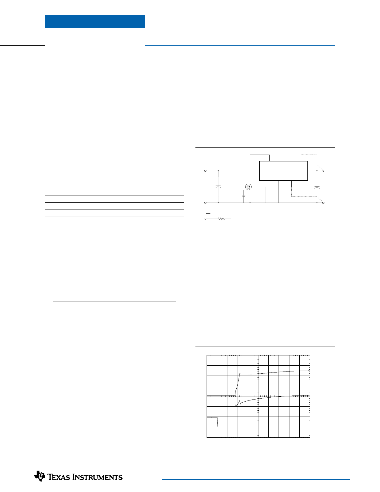
Turn-On Time: When the Remote On/Off input is left
open-circuit, the output of the converter is automatically
1
enabled when a valid input voltage
is applied to the
input power pins. The converter typically rises to full
regulation within 30ms of the application of power (or
after the release of the Remote On/Off pin with input
power applied). The actual turn-on time will vary with
the input voltage, output load, and the total amount of
capacitance connected to the output. Using the circuit of
Figure 1, Figure 2 shows the typical output voltage and
input current waveforms for a PT3322/PT4562 after Q
is turned off. The turn off of Q1 correlates with the fall
of the Q
Vgs waveform. The waveforms were measured
1
with a 48Vdc input voltage, and 5-A resistive load.
Figure 2
Vo (2V/Div)
Iin (0.5A/Div)
Q1Vgs (10V/Div)
o
o
1
HORIZ SCALE: 2ms/Div
For technical support and more information, see inside back cover or visit www.ti.com

Application Notes
PT3320/3340/4560/4580 Series
VDE Approved Installation Instructions (Installationsanleitung)
Nennspannnug (Rated Voltage): PT4560 36 to 72 Vdc, Transient to 75Vdc
PT4580 18 to 60 Vdc, PT4599 19 to 31 Vdc
Nennaufnahme (Rated Input): PT4560 1.5 Adc
PT4580, PT4599 3.0 Adc
Nennleistung (Rated Power): 30 Watts Maximum
Ausgangsspannung (Sec. Voltage): PT4560 Series PT4580 Series
PT4561, 3.3 Vdc, 8.0 Adc PT4581, 3.3 Vdc, 8.0 Adc
PT4562, 5.0 Vdc, 6.0 Adc PT4582, 5.0 Vdc, 6.0 Adc
Ausgangsstrom (Sec. Current): PT4563, 12.0 Vdc, 2.5 Adc PT4583,12.0 Vdc, 2.5 Adc
oder (or) PT4564, 15.0 Vdc, 2.0 Adc PT4584,15.0 Vdc, 2.0 Adc
Ausgangsleistung (Sec. Power): PT4565, 2.0 Vdc, 8.0 Adc PT4585, 1.8 Vdc, 8.0 Adc
PT4566, 2.5 Vdc, 8.0 Adc PT4599, 5.0 Vdc, 6.0 Adc
PT4567, 1.8 Vdc, 8.0 Adc
PT4568, 5.2 Vdc, 6.0 Adc
PT4569, 6.0 Vdc, 5.0 Adc
PT4570, 8.0 Vdc, 3.75 Adc
PT4571, 9.0 Vdc, 3.3 Adc
Angabe der Umgebungstemperatur
(Information on ambient temperature): +85°C Ambient or 100°C Case Maximum
Besondere Hinweise (Special Instructions):
Es ist vorzusehen, daß die Spannungsversorgung in einer Endanwendung über eine isolierte
Sekundaerschaltung bereit gestellt wird. Die Eingangspannung der Spannungsversorgungsmodule muss
eine verstaerkte Isolierung von der Wechselstromquelle aufweisen.
Die Spannungsversorgung muss gemaess den Gehaeuse-, Montage-, Kriech- und Luftstrecken-,
Markierungs- und Trennanforderungen der Endanwendung installiert werden. Bei Einsatz eines TNV-3Einganges muss die SELV-Schaltung ordnungsgemaess geerdet werden.
(The power supply is intended to be supplied by isolated secondary circuitry in an end use application.
The input power to these power supplies shall have reinforced insulation from the AC mains.
The power supply shall be installed in compliance with the enclosure, mounting, creepage, clearance,
casualty, markings, and segregation requirements of the end-use application. When the input is TNV-3,
the SELV circuitry must be reliably grounded.)
Offenbach,
VDE Prüf- und Zertifizierungsinstitut
Abteilung /
(Jürgen Bärwinkel)
Department TD
Ort /
Place
: Datum /
(Stempel und Unterschrift des Herstellers / Stamp
and signature of the manufacturer)
Date
:
For technical support and more information, see inside back cover or visit www.ti.com

IMPORTANT NOTICE
Texas Instruments Incorporated and its subsidiaries (TI) reserve the right to make corrections, modifications,
enhancements, improvements, and other changes to its products and services at any time and to discontinue
any product or service without notice. Customers should obtain the latest relevant information before placing
orders and should verify that such information is current and complete. All products are sold subject to TI’s terms
and conditions of sale supplied at the time of order acknowledgment.
TI warrants performance of its hardware products to the specifications applicable at the time of sale in
accordance with TI’s standard warranty . Testing and other quality control techniques are used to the extent TI
deems necessary to support this warranty . Except where mandated by government requirements, testing of all
parameters of each product is not necessarily performed.
TI assumes no liability for applications assistance or customer product design. Customers are responsible for
their products and applications using TI components. T o minimize the risks associated with customer products
and applications, customers should provide adequate design and operating safeguards.
TI does not warrant or represent that any license, either express or implied, is granted under any TI patent right,
copyright, mask work right, or other TI intellectual property right relating to any combination, machine, or process
in which TI products or services are used. Information published by TI regarding third–party products or services
does not constitute a license from TI to use such products or services or a warranty or endorsement thereof.
Use of such information may require a license from a third party under the patents or other intellectual property
of the third party , or a license from TI under the patents or other intellectual property of TI.
Reproduction of information in TI data books or data sheets is permissible only if reproduction is without
alteration and is accompanied by all associated warranties, conditions, limitations, and notices. Reproduction
of this information with alteration is an unfair and deceptive business practice. TI is not responsible or liable for
such altered documentation.
Resale of TI products or services with statements different from or beyond the parameters stated by TI for that
product or service voids all express and any implied warranties for the associated TI product or service and
is an unfair and deceptive business practice. TI is not responsible or liable for any such statements.
Mailing Address:
Texas Instruments
Post Office Box 655303
Dallas, Texas 75265
Copyright 2002, Texas Instruments Incorporated
 Loading...