

Page 1

User's Guide
SLAU658–March 2016
PGA411-Q1 EVM User's Guide
The PGA411-Q1 EVM allows users to evaluate the functionality of the PGA411-Q1 device. This user’s
guide describes both the hardware platform containing a sample PGA411-Q1 device, and the graphical
user interface (GUI) software used to configure the functionality and diagnostics on the PGA411-Q1
resolver-to-digital interface IC. In addition to evaluating the PGA411-Q1 device, the other objective of this
board is to display in the GUI the position (angle) or velocity readings from a resolver sensor.
This document also includes the EVM schematics, bill of materials, and PCB layout.
NOTE: Texas Instruments recommends using the PGA411-Q1 EVM user's guide (this document)
after reading and following the steps listed in the PGA411-Q1 Evaluation Module Quick Start
Guide. To download this guide, go to the product folder: www.ti.com/product/PGA411-Q1.
Contents
1 Introduction ................................................................................................................... 3
2 Setup and Operation ........................................................................................................ 3
2.1 Required Equipment for Device Evaluation ..................................................................... 3
2.2 Initial EVM Setup ................................................................................................... 3
2.3 GUI Software ........................................................................................................ 7
3 EVM Evaluation Examples................................................................................................ 16
3.1 EVM Checks for Proper Operation.............................................................................. 16
4 Schematics, Bill of Materials, and Layout............................................................................... 20
4.1 Schematics......................................................................................................... 21
4.2 Bill of Materials .................................................................................................... 23
4.3 Layout and Component Placement............................................................................. 27
1 PGA411-Q1 EVM Block Diagram.......................................................................................... 3
2 PGA411-Q1 EVM............................................................................................................ 4
3 PGA411-Q1 GUI Block Diagram........................................................................................... 5
4 PGA411-Q1 Device Startup Failed........................................................................................ 5
5 GUI PGA41x-Q1 EVM Main Screen ...................................................................................... 8
6 Device-State Status and Selection ........................................................................................ 8
7 Pin Configuration Screen ................................................................................................... 9
8 Memory Map................................................................................................................ 11
9 Bit Selection................................................................................................................. 11
10 Hex Selection (REG)....................................................................................................... 11
11 Search Box and Register Descriptions.................................................................................. 12
12 Data Monitor ................................................................................................................ 13
13 DEMO Screen .............................................................................................................. 14
14 Fault Status ................................................................................................................. 15
15 FAULTRES Change in Block Diagram .................................................................................. 16
16 FAULTRES Change in Pin Configuration Tab ......................................................................... 17
MSP430, E2E are trademarks of Texas Instruments.
Windows is a registered trademark of Microsoft Corporation.
All other trademarks are the property of their respective owners.
SLAU658–March 2016
Submit Documentation Feedback
List of Figures
Copyright © 2016, Texas Instruments Incorporated
PGA411-Q1 EVM User's Guide
1
Page 2

www.ti.com
17 Test Points for Exciter Outputs and Common Mode Voltage ........................................................ 18
18 OE1-OE2 Differential Output from the Exciter.......................................................................... 19
19 DEV_OVUV Register Bits Relevant to Exciter Amplifier Gain........................................................ 19
20 Exciter Amplifier Gain Change Using Memory Map ................................................................... 20
21 OE1-OE2 Differential Output from the Exciter With Updated Gain .................................................. 20
22 EVM Schematic............................................................................................................. 21
23 Schematic—Digital Interface.............................................................................................. 22
24 Top-Side Layout............................................................................................................ 27
25 Bottom-Side Layout ........................................................................................................ 27
List of Tables
1 Description of EVM Switches .............................................................................................. 6
2 Description of EVM Jumpers............................................................................................... 6
3 BOM.......................................................................................................................... 23
2
PGA411-Q1 EVM User's Guide
Copyright © 2016, Texas Instruments Incorporated
Submit Documentation Feedback
SLAU658–March 2016
Page 3

PGA411-Q1
USB
SINE
SPI <4>
PGA411-Q1 EVM
J7
5-V
V
IO
J6
EXCITER
J4
20-MHz XTAL
5 V
FAULT
FAULTRES
Data<N>
PGA411-Q1
GUI
From
Resolver
RESET
To
Resolver
COSINE
MSP430
www.ti.com
1 Introduction
The PGA411-Q1 evaluation module (EVM) is a board designed for the evaluation of the PGA411-Q1
resolver-to-digital interface IC from Texas Instruments. The PGA411-Q1 EVM incorporates all required
circuitry and components with the following features:
• PGA411-Q1 resolver-to-digital interface with power supply & amp
• Texas Instruments' MSP430™ microcontroller used for controlling the PGA411-Q1 device through the
I/O pins and a SPI port in addition to receiving digital data in different formats
• Voltage LDO regulator, TI's TLV716P, to provide configurable VIOvoltages (3.3 V or 1.8 V)
• Voltage LDO regulator, TI's TPS735, for the 3.3-V MSP430
• Circuitry for interfacing general resolver sensors
• 20-MHz XTAL as PGA411-Q1 single reference clock
• Multiple test points for main analog and digital signals
• UART, JTAG, and USB connectors
Figure 1 shows the PGA411-Q1 EVM architecture, where the key components and blocks previously listed
can be identified.
Introduction
2 Setup and Operation
2.1 Required Equipment for Device Evaluation
The following elements are required for proper operation and to receive consistent results with this user's
guide:
• A single power supply that is capable of 5-V operation and a minimum current of 0.5 A
• A computer with Windows®XP or Windows 7 and .net Framework 4.0 or later
• The PGA411-Q1 GUI
• A resolver sensor connected to the correct ports. Refer to the resolver data sheet for more information.
2.2 Initial EVM Setup
2.2.1 Installing Graphical User Interface Software
Before the PGA411-Q1 device can be evaluated the GUI software must be available on a host computer.
Run the GUI installer and place the executable file in a convenient location (Desktop or c:\Texas
Instruments EVM\) and double click to run the application.
To download the PGA411-Q1 GUI go to www.ti.com/product/PGA411-Q1.
SLAU658–March 2016
Submit Documentation Feedback
Figure 1. PGA411-Q1 EVM Block Diagram
Copyright © 2016, Texas Instruments Incorporated
PGA411-Q1 EVM User's Guide
3
Page 4
NRST
(S3)
FAULT_RES
(S2)
MCU_RST (S4)
USB
(J15)
5-V
DC
J2
(1-2)
J3
(3-4)
J10
J5
(3-5, 4-6)
J7
Resolver Sensor
Connections
J6
J4
J11
1
2
S1
PGA411-Q1
MSP430
LED USB_RDY
(D12)
Setup and Operation
2.2.2 Set-Up Instructions
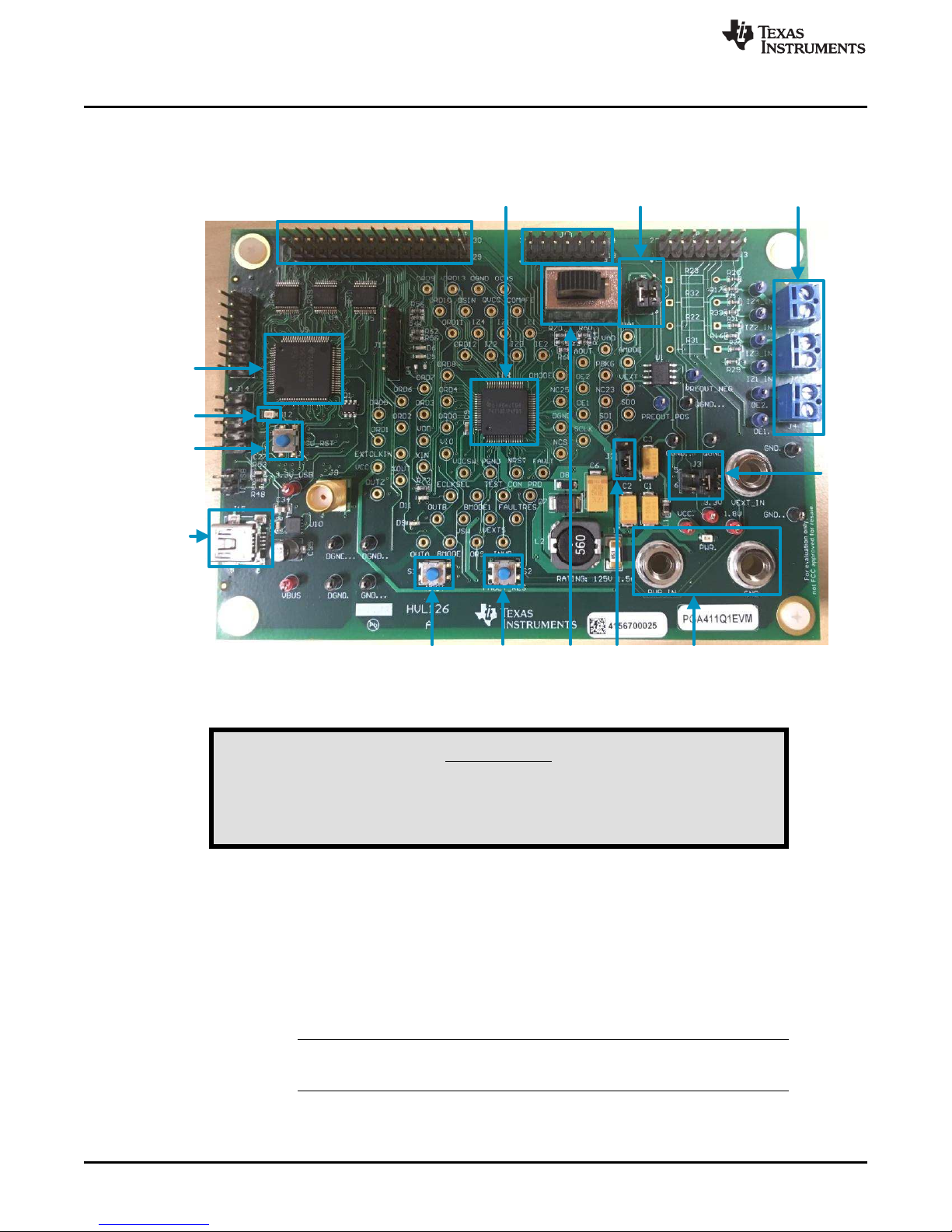
For set-up instructions, refer to Figure 2.
www.ti.com
Figure 2. PGA411-Q1 EVM
This EVM contains components that are sensitive to Electrostatic
Discharge (ESD). Use proper laboratory techniques and equipment
WARNING
to minimize the chance of an ESD or EOS event.
Step 1. Set up EVM jumpers as follows:
• Confirm the J3 jumper settings (3-4) for 3.3-V VIO. This step is required for proper
operation with the MSP430 device.
• Confirm the J5 jumper settings (3-5 and 4-6) to connect the exciter outputs (OEx pins) to
the IEx input pins. The tracking loop inside the PGA411-Q1 device must sense the
exciter outputs.
• Confirm that the J2 jumper is present to connect the internal boost supply to the supply
input of the integrated exciter amplifier (VEXT).
NOTE: Using the integrated boost supply for the exciter amplifier is strongly
recommended.
Step 2. Apply the 5-V supply to the banana connectors for VCCand GND.
4
PGA411-Q1 EVM User's Guide
Copyright © 2016, Texas Instruments Incorporated
Submit Documentation Feedback
SLAU658–March 2016
Page 5
Reset
www.ti.com
Setup and Operation
Step 3. Connect the USB cable to the EVM and to the PC.
NOTE: Power, as described in Step 2, must be applied before connecting the USB.
Step 4. Verify that the LED USB_RDY (D12) is on, ensuring a good connection. If it is blinking or off,
unplug and replug the USB cable, and press the MCU reset, MCU_RST (S4).
Step 5. Launch the PGA411-Q1 GUI.
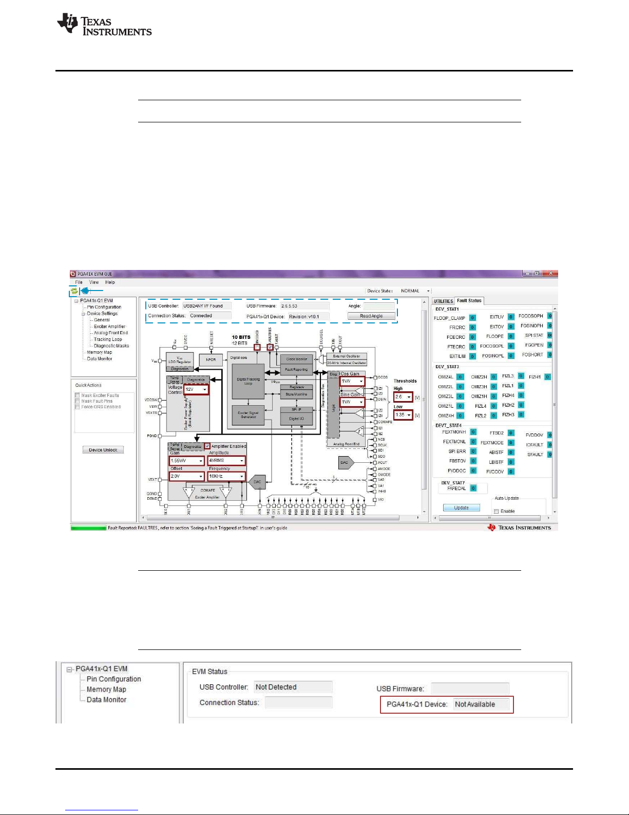
Step 6. Wait a few seconds after the GUI welcome screen appears. The first view should be of a
block diagram which is a high level representation of the PGA411-Q1 resolver-to-digital
interface and contains interactive features. The red boxes indicate controls that can be used
to configure internal blocks inside the PGA411-Q1 device.
If the connection is successful, the Connection Status field displays Connected and a revision number
is displayed in the PGA411-Q1 Device field as shown in Figure 3. If the connection process failed,
press the S4 switch on the EVM and then press the Reset button in the upper left corner of the GUI
(see Figure 3) to restart the connection.
NOTE: Follow the start-up procedure carefully and ensure that board connections are correct. The
power must be applied before the USB cable is plugged in. The USB_RDY LED close to the
MSP430 controller should remain on continuously after connecting the USB cable and
should not blink. If the device does not power up properly, the EVM status field in the GUI
will display: PGA41x-Q1 Device: Not Available as shown in Figure 4. If this occurs, turn off
the 5-V power supply, unplug the USB cable, and go back to Step 2.
Figure 4. PGA411-Q1 Device Startup Failed
SLAU658–March 2016
Submit Documentation Feedback
Figure 3. PGA411-Q1 GUI Block Diagram
Copyright © 2016, Texas Instruments Incorporated
PGA411-Q1 EVM User's Guide
5
Page 6
Setup and Operation
2.2.2.1 EVM Switches and Jumpers Settings
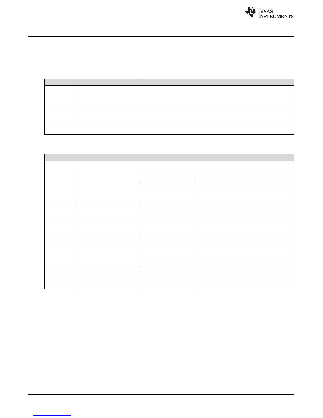
Refer to Figure 2 for the locations of the switches and jumpers on the PGA411-Q1 EVM.
Table 1 lists the descriptions of the EVM switches. Table 2 lists the descriptions of the EVM jumpers.
Table 1. Description of EVM Switches
Switch (SW) Description
0: This position is the default and selects the prepopulated IZx resistive divider
S1 Voltage divider
S2 Fault reset
S3 Device reset This switch pulls the NRST pin low. This action resets the PGA411-Q1 device.
S4 MSP430 BSL This switch resets the MSP430 microcontroller. The firmware is reloaded.
(30 kΩ / 30 kΩ).
1: This position selects the user-populated IZx resistive divider (30 kΩ / external
resistor value).
This switch pulls the FAULTRES pin low when pressed. When this switch is
pressed and then released, all faults from the PGA411 device are cleared.
Table 2. Description of EVM Jumpers
Jumper No. Function State Description
J2 VEXT Jumper
J3 VIO SELECT
J4 OEx Terminal
J5 OEx to IEx
J6 COS IZx terminal
J7 SIN IZx terminal
J10 Analog Connector — Header for analog signals
J11 Digital Connector — Header for digital signals
J15 USB Connector — Connector for USB cable
Open Disconnect VEXT from boost output
Closed (Default) Connect VEXT to boost output
1-2 Do not use
3-4 (Default) VIO = 3.3 V
5-6
Pin 1 Exciter output 1 to resolver (OE1)
Pin 2 Exciter output 2 to resolver (OE2)
3-5 (Default) Connect OE1 to IE1 through voltage divider
4-6 (Default) Connect OE2 to IE2 through voltage divider
All other combinations Do not use
Pin 1 Input to IZ1 external filter
Pin 2 Input to IZ3 external filter
Pin 1 Input to IZ2 external filter
Pin 2 Input to IZ4 external filter
VIO = VCC (5 V), Do not use with current EVM
version. This mode is to interface PGA411-Q1
device with external microcontrollers.
www.ti.com
6
PGA411-Q1 EVM User's Guide
Copyright © 2016, Texas Instruments Incorporated
Submit Documentation Feedback
SLAU658–March 2016
Page 7

www.ti.com
2.3 GUI Software
2.3.1 PGA41x-Q1 GUI Main Screen
Figure 5 shows the default starting screen of the PGA41x-Q1 GUI. If the EVM is connected properly, the
screen should display the values that follow for the EVM Status fields, as described in Step 5 in
Section 2.2.2:
• USB Controller: USB2ANY I/F Found
• USB Firmware: 2.6.5.53 (this value is designed for Revision B of the EVM)
• Connection Status: Connected
• PGA41x-Q1 Device: Revision: v10.1
The default GUI view is the block diagram of the PGA411-Q1 resolver-to-digital interface IC and contains
interactive features. All boxes in red, as shown in Figure 5, are controls that can be configured. These
boxes indicate the default values of the PGA411-Q1 device after power on. The configurable elements in
this block diagram include:
• Internal boost voltage control
– Boost output voltage from 10 to 17 V
• Exciter amplifier
– Exciter frequency (10 to 20 kHz)
– Exciter amplitude (4 V
– Exciter amplifier gain (1.15 to 1.9 V/V )
– Common-mode offset (0.5 to 2 V)
Use a scope probe on the test points next to exciter connection, J4, to view changes to these
blocks instantaneously. The optimum values depend on the characteristics of the resolver sensor
that is used.
• Analog front end (AFE)
– COS gain and SIN gain from 0.75 to 3.5 V/V.
– Diagnostic values for detection thresholds on the AFE amplifiers. These values include both the
high and low thresholds.
The optimum AFE settings depend on the signal levels from the resolver outputs (sine and cosine).
Observe these signals on the test points next to the J6 and J7 jumpers when configuring the AFE.
RMS
or 7 V
RMS
Setup and Operation
(1)
)
NOTE: Both gains must match to achieve better accuracy on the angle estimation.
• Read Angle button
When pressed, the angle (in degrees) is displayed, if the resolver sensor is rotated and read again, the
value should update.
• BMODE0 which is the control bit for 10-bit and 12-bit modes
Higher precision is achieved by changing the resolution from 10 bits to 12 bits by checking the
BMODE0 box. The new angle reading should have more digits of precision.
• Control bit for the FAULTRES pin
To ignore faults, ensure that the FAULTRES pin is set to low. To set this pin low, uncheck the box.
NOTE: Toggling the FAULTRES pin with a fault condition still present causes the PGA411-Q1
device to go into normal operation, which may cause damage to the PGA411-Q1 device.
This is most likely to occur with high current short circuits on the exciter amplifier.
Ignoring the faults is only recommended for initial evaluation.
(1)
This version is the latest at the time this user guide was generated.
SLAU658–March 2016
Submit Documentation Feedback
Copyright © 2016, Texas Instruments Incorporated
PGA411-Q1 EVM User's Guide
7
Page 8
Setup and Operation
2.3.2 Device State
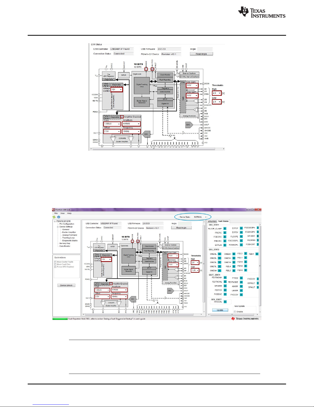
The Device State menu (see Figure 6) supports two device states: NORMAL and DIAGNOSTICS. This
menu displays the current device state. Click on the down arrow for the dropdown menu to select a new
state. This menu always displays the current device state, therefore serving as a confirmation that the
device transitioned to the new state correctly.
www.ti.com
Figure 5. GUI PGA41x-Q1 EVM Main Screen
Figure 6. Device-State Status and Selection
NOTE: The data sheet includes a detailed description on why and how to change between these
states. Some of the controls in the PGA411-Q1 GUI interactive block diagram change states,
from NORMAL to DIAGNOSTIC in a hidden manner to make the configuration changes (for
example, changing the exciter sine-wave amplitude from 4 V
for more details.
8
PGA411-Q1 EVM User's Guide
RMS
Copyright © 2016, Texas Instruments Incorporated
to 7 V
). See Section 2.3.4
RMS
Submit Documentation Feedback
SLAU658–March 2016
Page 9
www.ti.com
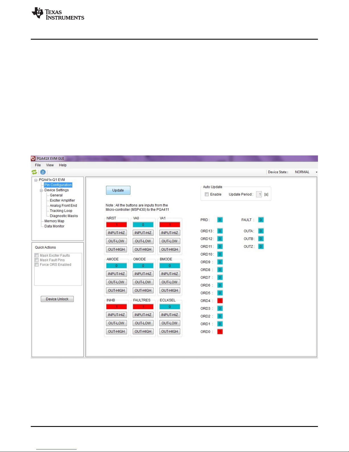
2.3.3 Pin Configuration and Fault Register Status
The Pin Configuration window (see Figure 7) displays the current status of the digital input and output
pins. The input pins of the PGA411-Q1 device are shown in Figure 7 on the left-side (below the Update
button) in the GUI, where the low or high values will be driven by the MSP430. Select the status of the
nine digital-input pins by clicking on the appropriate button (INPUT-HiZ, OUT-LOW, or OUT-HIGH). The
MSP430 device then switches the connected I/O pin to the selected value.
The output pins of the PGA411-Q1 device are displayed to the right of the group of input pins. This section
displays the current status of the output pins with logic low equal to 0 and logic high equal to 1. For
example if the FAULT pin changes to HIGH the GUI displays a 1 in the field which is then highlighted in
red.
The Fault Status tab on the right-side of the Pin Configuration window displays the current status of the
device registers which report any fault in the system. The following sections provide more details on the
fault status registers.
The display updates each time the Update button is pressed. To automatically update this page, check the
Enable box under the Auto Update section and select an update period in 1-s increments.
Setup and Operation
SLAU658–March 2016
Submit Documentation Feedback
Figure 7. Pin Configuration Screen
Copyright © 2016, Texas Instruments Incorporated
PGA411-Q1 EVM User's Guide
9
Page 10

Setup and Operation
2.3.4 Memory Map
The memory map is used to read and write to all of the device registers. The Memory Map window (see
Figure 8) includes the register name, hex value for all 16 bits, and individual bit values.
A change to a register value occurs in one of two ways. The first way is bit by bit. To change a register
value in this way, click in the text field of the bit number that will change. If this text field displays a 0, click
the text field to toggle the value to 1 (see Figure 9). To update more bits, repeat the procedure. The
second way to update a bit is with the hex value. Click on the hex value under the REG column (see
Figure 10) and type the new HEX value.
In each case, after updating the register values the row should become highlighted in yellow, which
indicates that the change has not yet been programmed to the PGA411-Q1 device.
To program the new register values into the device, click on the Write Selected button to updated only the
highlighted registers. Click on the Write All buttons to modify all registers at one time.
NOTE: The device must be in diagnostics mode to write to the majority of registers. Refer to the
PGA411-Q1 data sheet for the entire list of registers.
The primary buttons at the bottom of this window are defined as follows:
Read Selected —After selecting the register by clicking on the register name while holding the CTRL key
for multiple selection, use this button to read all of the selected registers.
Write Selected —After selecting the register by clicking on the register name while holding the CTRL key
for multiple selection, use this button to write to all of the selected registers.
www.ti.com
Read All —Use this button to read all of the registers and to update the register values in the table.
Write All —Use this button to write the current values listed in the table to all of the registers, including
those that were not modified.
ZERO GRID —Use this button to set all registers to zero.
DESELECT GRID —Use this button to remove all selections from the grid.
SAVE GRID —Use this button to save the contents of the grid to a text file. This option is useful for
reusing register settings that were predefined.
LOAD GRID —Use this button to load the grid with the contents of a text file.
10
PGA411-Q1 EVM User's Guide
Copyright © 2016, Texas Instruments Incorporated
Submit Documentation Feedback
SLAU658–March 2016
Page 11

www.ti.com
Setup and Operation
Figure 8. Memory Map
Figure 9. Bit Selection Figure 10. Hex Selection (REG)
SLAU658–March 2016
Submit Documentation Feedback
Copyright © 2016, Texas Instruments Incorporated
PGA411-Q1 EVM User's Guide
11
Page 12

Setup and Operation
2.3.4.1 Search Box and Register Descriptions on UTILITIES Tab
The bottom of the GUI includes a useful tool to search the contents of each register. For example, to find
the register that sets the exciter amplifier mode to 7 V
, type 7V in the Search Registers text field and
RMS
click on the Search button. Next, a list of all registers that include any description containing the keyword
7V displays below the search box.
Click on the corresponding register value inside the memory map to view the register description on the
UTILITIES tab on the right-hand side of the GUI. If DEV_PHASE_REG is selected, the UTILITIES tab
displays that bits 11-10 set the exciter mode (EXTMODE). The value for 7 V
In the same UTILITIES tab, the bottom-section of the tab includes a numeric base converter with hex,
decimal, and binary modes.
is 01. Refer to Figure 11.
RMS
www.ti.com
Figure 11. Search Box and Register Descriptions
12
PGA411-Q1 EVM User's Guide
Copyright © 2016, Texas Instruments Incorporated
Submit Documentation Feedback
SLAU658–March 2016
Page 13

www.ti.com
2.3.5 Data Monitor
The Data Monitor window (see Figure 12) plots the output angle or velocity information and provides
access to a Demo mode that shows the angle and velocity in an instrument cluster display. The fields and
buttons on this window are described as follows:
Data Capture Source — This field selects between SPI register read, USB, or UART burst reading.
NOTE: The UART mode requires additional hardware setup which is not included in the
Data Monitor — Use this field to select either the angle or velocity to plot.
Resolution — Use this field to select the resolution to export the data as.
Record Length — Use this field to select the number of data samples to plot on the graph.
Loop — If checked, when the graph fills up, selecting this checkbox clears the current graph and begin a
new graph.
RUN — This button starts reading the angle or velocity data.
Clear Plot — This button clears the plot.
Export Data — This button exports the data to a .txt file in comma separated value (CSV) format.
Setup and Operation
EVM package. For evaluation purposes, the UART mode is not required.
NOTE: The GUI was designed to support three modes of reading data from the PGA411-Q1
device. The collected samples could have some non-linearity when using the GUI to
read the angle registers. If a delay occurs in the waveform on the Data Monitor
window when reading the angle value, the delay is because of SPI. The EVM can
support faster data capture by omitting the USB-to-SPI circuit (using MSP430) and
connecting the controller directly to the digital pins available on the board. For
evaluation purposes, TI recommends using SPI.
SLAU658–March 2016
Submit Documentation Feedback
Figure 12. Data Monitor
Copyright © 2016, Texas Instruments Incorporated
PGA411-Q1 EVM User's Guide
13
Page 14

Setup and Operation
Demo — Use this button to access the high resolution instrument cluster Display for instantaneous angle
and velocity display. Click on the ESC button on the keyboard to exit this mode. Refer to Figure 13.
www.ti.com
Figure 13. DEMO Screen
NOTE: The velocity resolution is limited to 500 rpm.
To properly read the velocity, calibrate the system by clicking the Calibrate button. For
detailed information, refer to Troubleshooting Guide for PGA411-Q1 (SLAA687).
If the fault sign appears in the demo mode (in the form of a warning sign), refer to
Section 2.3.6 to clear the faults.
NOTE: Unlocking the EEPROM device functionality found under the general tab is not currently
available in the current version of the PGA411-Q1 EVM GUI. This functionality will be added
in a future version.
14
PGA411-Q1 EVM User's Guide
Copyright © 2016, Texas Instruments Incorporated
Submit Documentation Feedback
SLAU658–March 2016
Page 15
www.ti.com
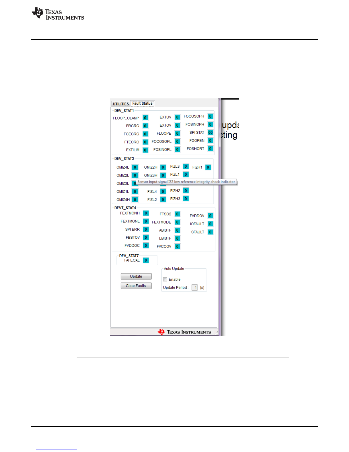
2.3.6 Fault Status
The Fault Status tab (see Figure 14) displays the status of the PGA411-Q1 fault bits. Click the Update
button to refresh the display the current fault status. This tab can be configured to automatically update by
selecting the Enable checkbox in the Auto Update section and setting the update period in 1-s increments.
The PGA411-Q1 device detects a fault in the system when any bit or group of bits displays a 1 and the
color of the text field changes to red. Placing the mouse cursor on top of the status bit displays a text box
with information on the fault, as shown in Figure 14.
Setup and Operation
NOTE: Make sure the FAULTRES pin is HIGH to view the faults (see Section 2.3.1).
If the auto update option is enabled, only the SFAULT may appear because faults are
cleared when read. The SFAULT gives the state of the fault pin.
SLAU658–March 2016
Submit Documentation Feedback
Figure 14. Fault Status
Copyright © 2016, Texas Instruments Incorporated
PGA411-Q1 EVM User's Guide
15
Page 16
EVM Evaluation Examples
3 EVM Evaluation Examples
3.1 EVM Checks for Proper Operation
3.1.1 Fault Triggered at Startup
The resolver setup may trigger faults because of specific requirements on voltage or current. To
understand the primary cause, ignore the faults and continue with the initial evaluation.
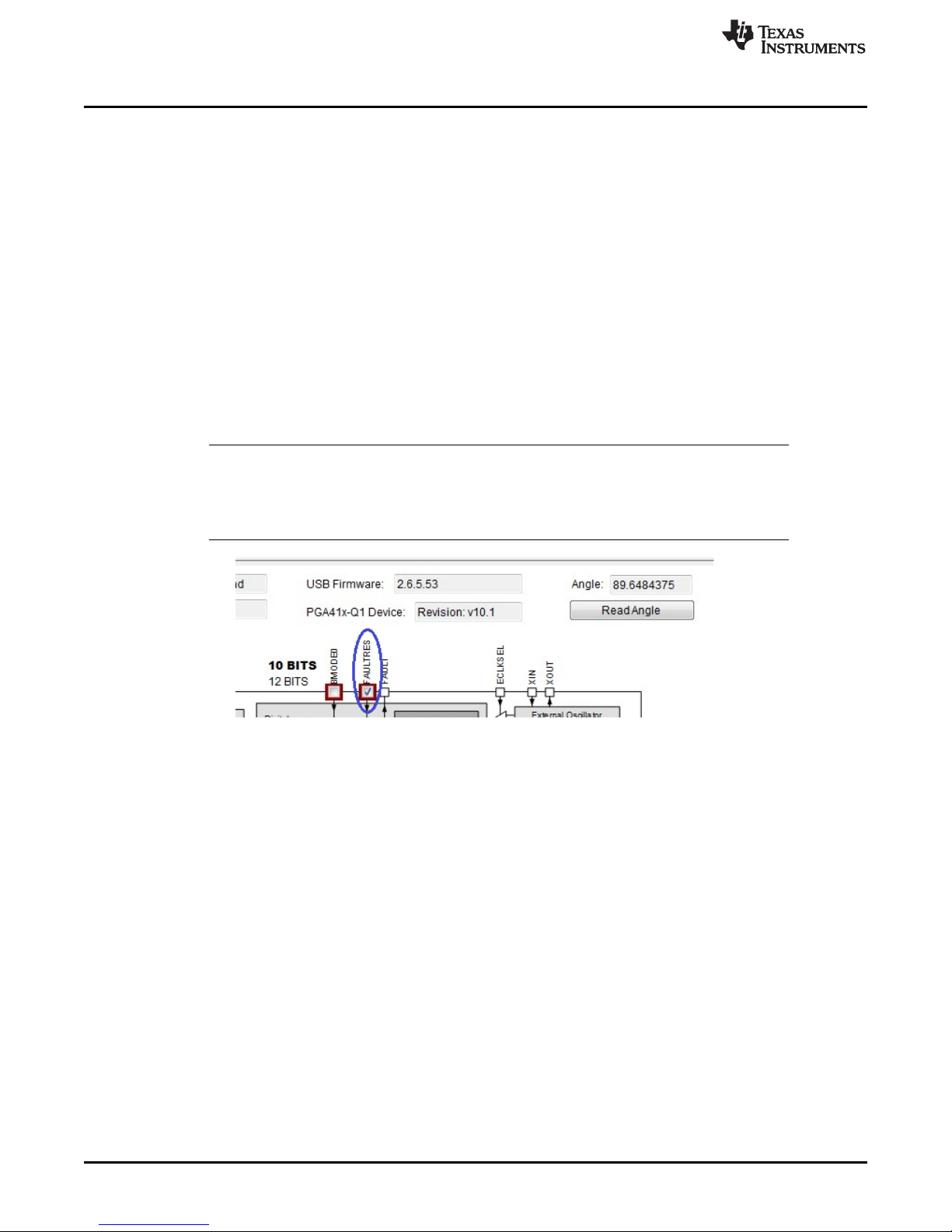
If a fault appears when the GUI is first executed after properly connecting the device EVM as
recommended in Section 2.2.2, the PGA411-Q1 device can be set to ignore the faults. Setting the device
to ignore these faults can occur in two different ways:
• Using the PGA411-Q1 block diagram
Set the FAULTRES pin to low by unchecking the box in the block diagram as shown in Figure 15.
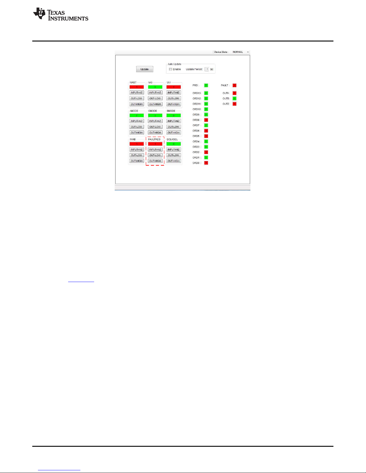
• Using the Pin Configuration tab
Set the FAULTRES bit low by clicking the OUT-LOW button as shown in Figure 16. This setting allows
for further evaluation of the resolver EVM.
NOTE: Toggling the FAULTRES pin with a fault condition still present causes the PGA411-Q1
device to go into normal operation, which may cause damage to the PGA411-Q1 device.
This is most likely to occur with high current short circuits on the exciter amplifier.
Ignoring the faults is only recommended for initial evaluation.
www.ti.com
Figure 15. FAULTRES Change in Block Diagram
16
PGA411-Q1 EVM User's Guide
Copyright © 2016, Texas Instruments Incorporated
Submit Documentation Feedback
SLAU658–March 2016
Page 17
www.ti.com
EVM Evaluation Examples
Figure 16. FAULTRES Change in Pin Configuration Tab
3.1.2 Changing Exciter Signal Pre-Amplifier Gain
Changing the exciter amplifier gain can occur using the PGA411-Q1 block diagram as explained in
Section 2.3.1; however, this section focuses on same procedure using the Memory Map tab which is more
descriptive of how a controller interfaces with the PGA411-Q1 device for this type of operation.
In the preamplifier block, the amplification level of the exciter signal can be adjusted while the common
mode voltage is defined by the voltage at the COMAFE pin (typically 2.5 V). The preamplifier gain is
selectable though the EXTOUT_GL[15:12] bits in the DEV_OVUV1 register and affects both the
preamplifier ORS output and power amplifier output. For more information, refer to the PGA411-Q1 data
sheet, SLASE76.
Step 1. In the GUI, select the Memory Map tab. This section is the primary form of control for the
device registers. For the bit definitions, see the PGA411-Q1 data sheet. The Information box
on the right-side of the window also displays the bit definitions.
Step 2. Change the state of the device to DIAGNOSTICS mode. Refer to Figure 19 and
Section 2.3.2.
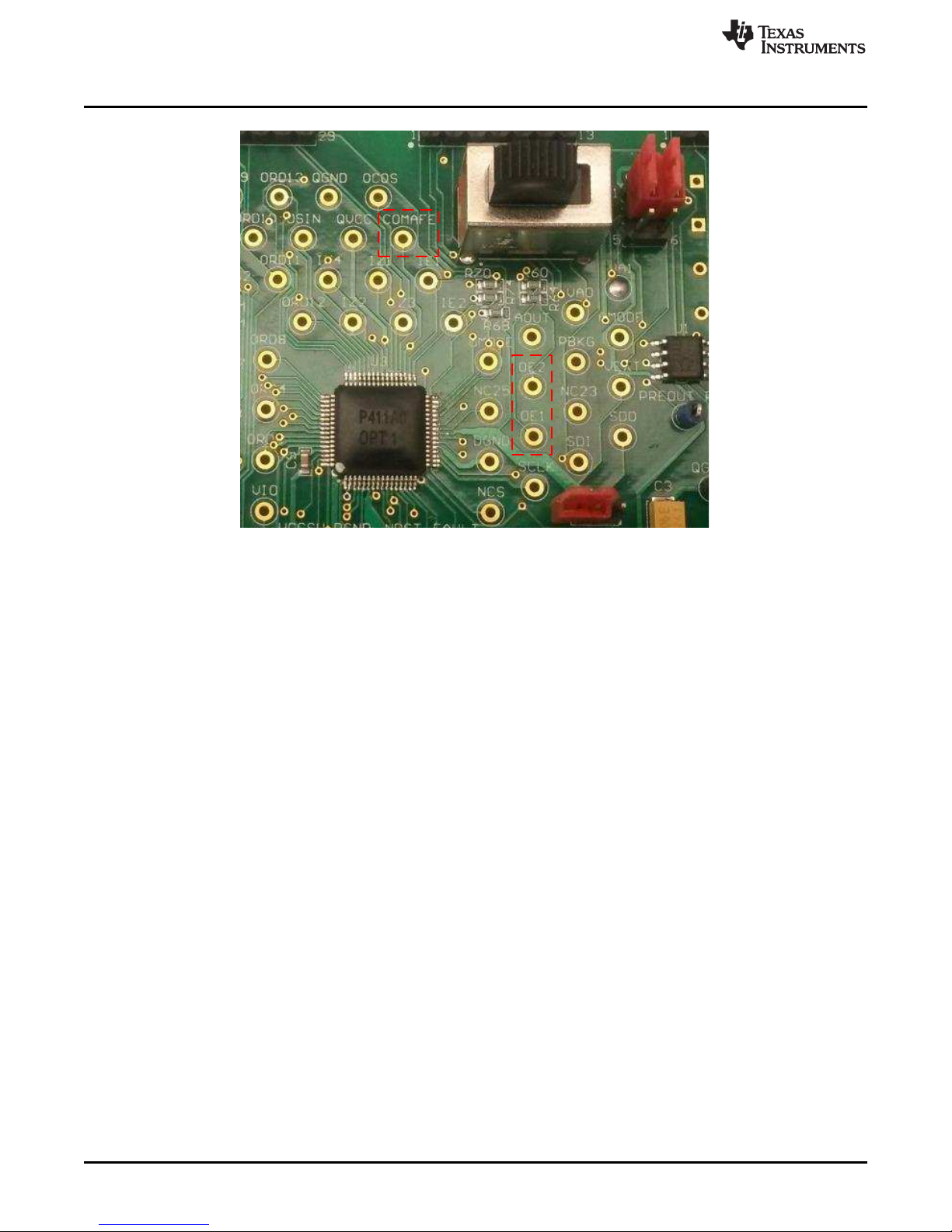
Step 3. Probe pins COMAFE to check the 2.5-V pin voltage and use a differential probe on the OE1
and OE2 pins. Figure 17 shows these test-point locations on the board.
OE1 —OE1 is the positive output of the exciter amplifier.
OE2 —OE2 is the negative output of the exciter amplifier.
SLAU658–March 2016
Submit Documentation Feedback
Copyright © 2016, Texas Instruments Incorporated
PGA411-Q1 EVM User's Guide
17
Page 18
EVM Evaluation Examples
Figure 17. Test Points for Exciter Outputs and Common Mode Voltage
www.ti.com
18
PGA411-Q1 EVM User's Guide
Copyright © 2016, Texas Instruments Incorporated
Submit Documentation Feedback
SLAU658–March 2016
Page 19
www.ti.com
EVM Evaluation Examples
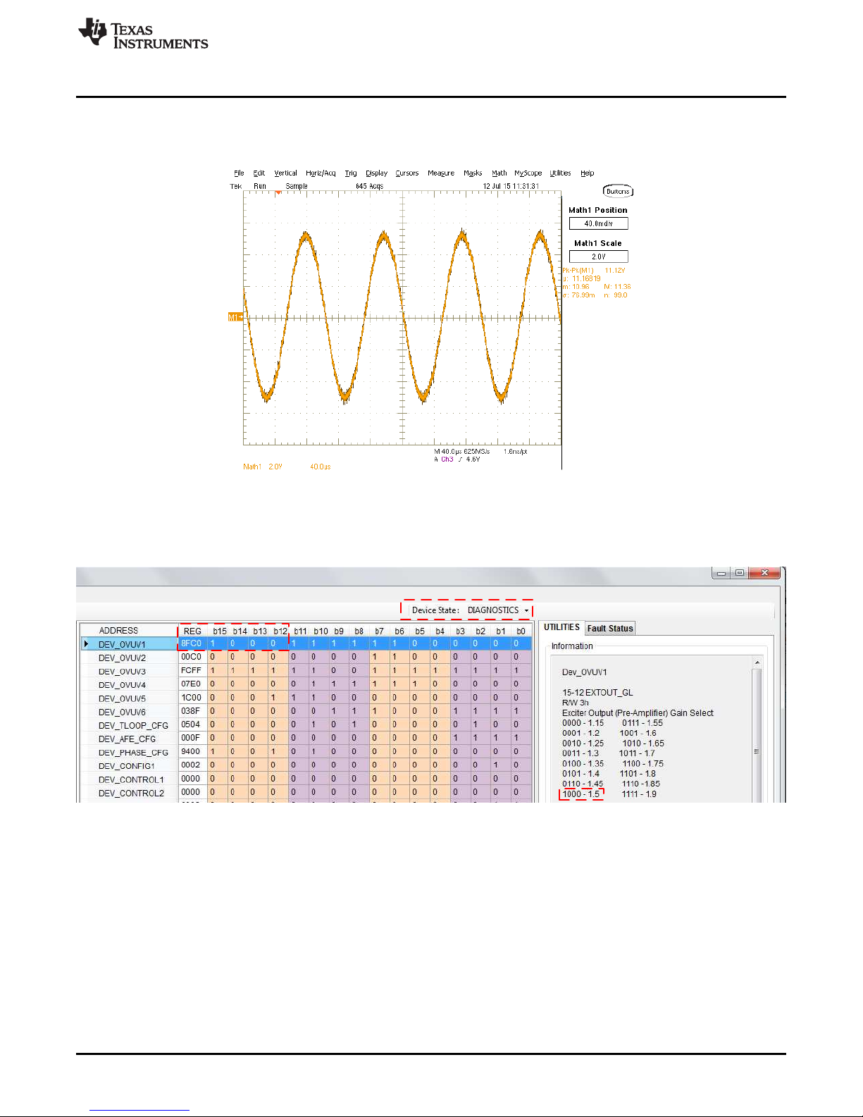
Step 4. Connect the scope probe to OE1 and compare this waveform to the one shown in Figure 18.
In this waveform, the peak-to-peak voltage of the differential voltage output of the exciter is
11.12 VPP.
Figure 18. OE1-OE2 Differential Output from the Exciter
Step 5. Click on the DEV_OVUV1 address inside the register map as shown in Figure 19. Text
should appear in the Information box on the UTILITIES tab. This box displays information
regarding the bits in the DEV_OVUV1 address.
Figure 19. DEV_OVUV Register
Bits Relevant to Exciter Amplifier Gain
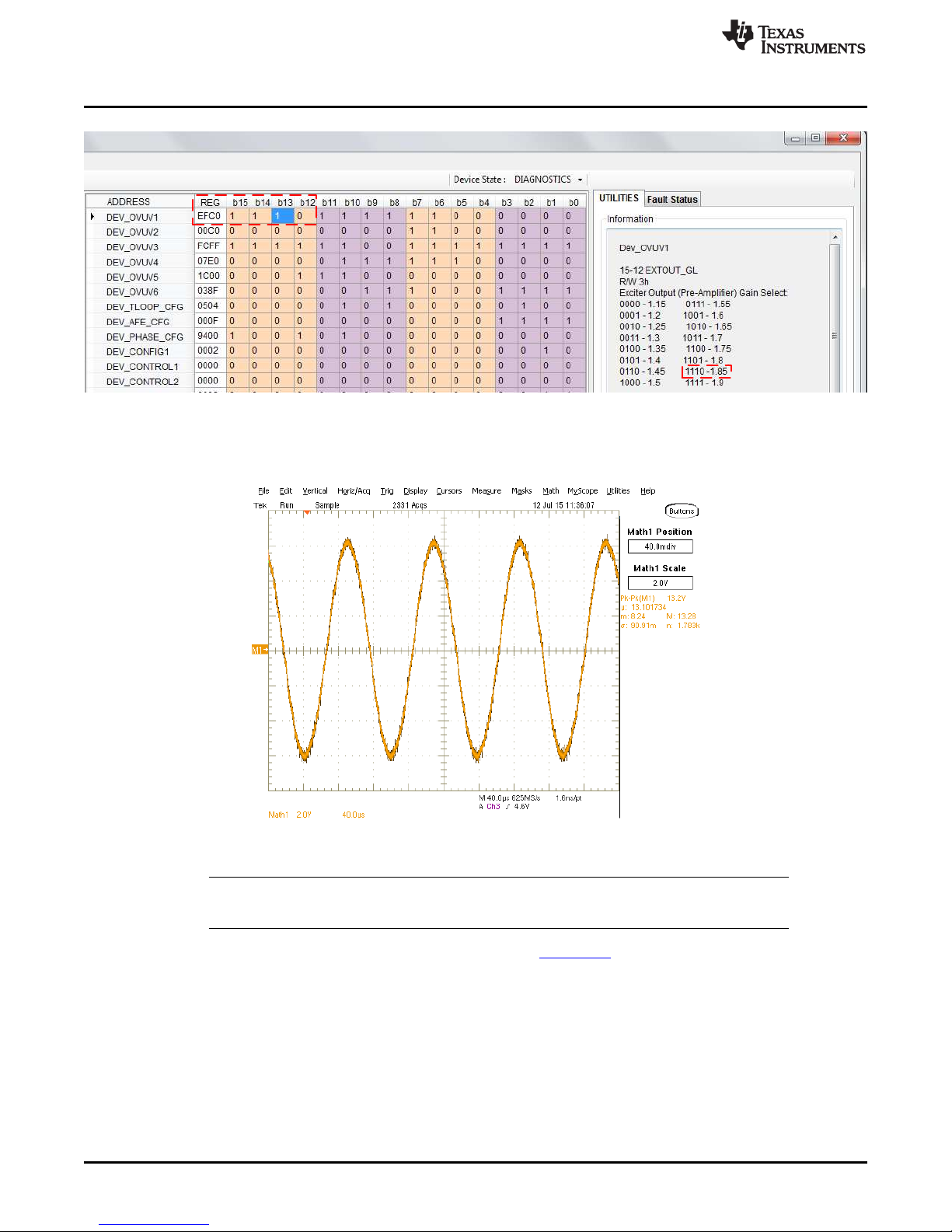
Step 6. Click the b14 and b13 bits to change the value inside the cell. To change the exciter
preamplifier gain from 1.5 V/V to 1.85 V/V, update the value of bits b15 through b12 to 1110
and write this register to the PGA411-Q1 device using the Write Selected button as explained
in Section 2.3.4.1. New bit values appear as shown in Figure 20.
SLAU658–March 2016
Submit Documentation Feedback
Copyright © 2016, Texas Instruments Incorporated
PGA411-Q1 EVM User's Guide
19
Page 20
Schematics, Bill of Materials, and Layout
Figure 20. Exciter Amplifier Gain Change Using Memory Map
Step 7. As shown in Figure 21, the amplitude of the waveform increased to approximately 13 V which
corresponds with the new programmed gain of the exciter amplifier.
www.ti.com
Figure 21. OE1-OE2 Differential Output from the Exciter With Updated Gain
NOTE: This example provides a step-by-step guide on how to change key parameters on the
PGA411-Q1 device using the memory map functionality.
For support questions, go to TI's E2E™ online community, e2e.ti.com.
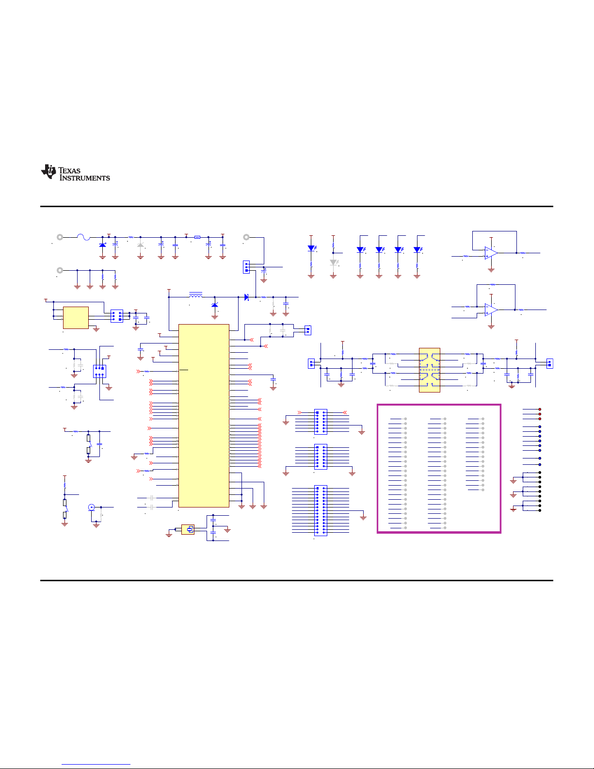
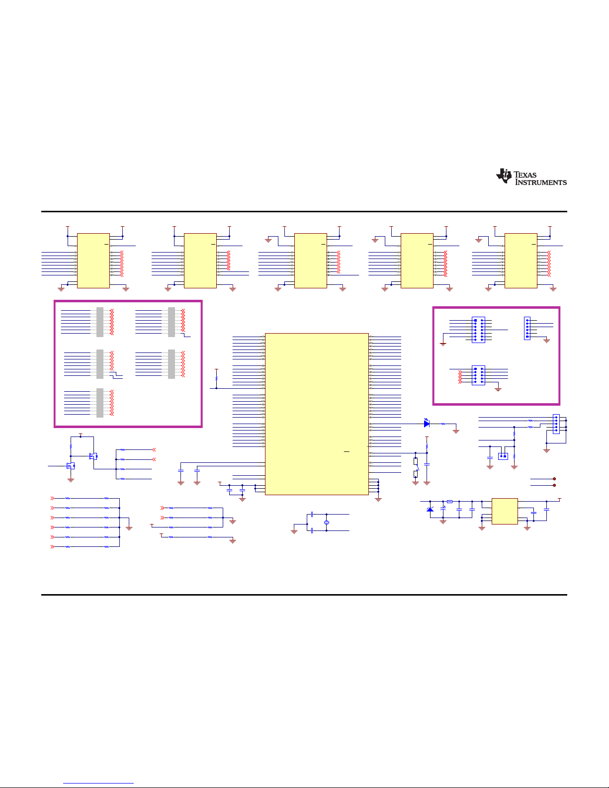
4 Schematics, Bill of Materials, and Layout
This section provides a detailed description of the schematic, bill of materials (BOM), and layout.
20
PGA411-Q1 EVM User's Guide
Copyright © 2016, Texas Instruments Incorporated
Submit Documentation Feedback
SLAU658–March 2016
Page 21
ORD9
48
FAULTRES
14
ORD12
45
NCS
17
IZ4
42
SDO
20
QVCC
39
NC
23
OE2
26
OMODE
29
VA1
32
COMAFE
35
PRD
15
FAULT
16
ORD11
46
ORD10
47
OSIN
43
ORD13
44
DGND
21
OE1
22
QGND
40
IZ2
41
IZ3
37
IZ1
38
NC
25
AMODE
28
VA0
31
AOUT
30
IE1
34
OCOS
36
PBKG
27
IE2
33
TEST
11
PGND
8
BMODE0
5
OUTB
2
INHB
13
SCLK
18
SDI
19
VEXT
24
RESET
12
ORS
9
VSW
6
BMODE1
7
ECLKSEL
3
OUTA
1
VEXTS
10
VCCSW
4
ORD8
49
ORD7
50
ORD6
51
ORD5
52
ORD4
53
ORD3
54
ORD2
55
ORD1
56
ORD0
57
OUTZ
64
EXTCLKIN
59
XOUT
63
VIO
61
XIN
62
VCC
60
VDD
58
PAD
65
U3
PGA411PAP
56uH
L2
20V
D8
PGND
J4 OEx
QGND
OE1
4.99k
R34
DNP
QGND
40.2k
R33
OE2
PGND
ORD0
ORD1
ORD2
ORD3
ORD4
ORD5
ORD6
ORD7
ORD8
ORD9
ORD10
ORD11
ORD12
ORD13
PRD
OUTZ
OUTB
OUTA
NCS
SCLK
SDI
SDO
EXTCLKIN
FAULT
AMODE
OMODE
INHB
ECLKSEL
VA0
VA1
VCC
VIO
VIO
OE2
OE1
1
34
2
G
G
Y1
GND
GND
XOUT
XIN
XIN
XOUT
15pF
C24
15pF
C25
C22
DNP
DNP
C23
DNP
DNP
VCC
GND
VEXT
J17
PWR_IN
PGND
J19
GND
GND PGND QGNDDGND
0R90
R10
GND GND QGND QGND
1000 ohm
L1
QVCC
QVCC
QGND DGND
C14
DNP
DNP
C20
DNP
DNP
1.2k
R4
FAULT
OCOS
COMAFE
OSIN
AOUT
ORS
0.1µF
C11
4.99k
R24
DNP
40.2k
R15
C10
DNP
DNP
R14
DNP
DNP
VOUT1
1
VOUT2
2
GND
3
EN2
4
VIN
5
EN1
6
U2
TLV7163318PDPQR
GND
12
34
56
J3
VCCSW
VIO
1µF
C8
DGND
0.1µF
C9
3.3V
1.8V
1
2
3
4
S3
VIO
GND
10k
R37
0.01µF
C21
NRST
TEST_CON
FAULTRES
Green
1
2
D3
VCC
GND
1.2k
R3
0
R36
DGND
10.0k
R11
10.0k
R12
ORS
COMAFE
10.0k
R2
ORS
QGND
QGND
QVCC
QVCC
0
R13
0
R1
PREOUT_NEG
PREOUT_POS
2
1
5
3
4
6 7
8
9
10
11
12
S1
30.0k
R26
J6
470pF
C12
QVCC
1000pF
C17
1000pF
C18
470pF
C13
20.0k
R30
30.0k
R28
30.0k
R19
30.0k
R21
30.0k
R18
30.0k
R20
30.0k
R27
30.0k
R25
IZ3
IZ1 IZ2
IZ4
QGND
QVCC
1000pF
C16
1000pF
C15
20.0k
R29
J7
R22
DNP
DNP
R31
DNP
DNP
R32
DNP
DNP
R23
DNP
DNP
0.01µF
C19
QGND
J9
R35
DNP
DNP
DGND
EXTCLKIN
QGND
QVCC
IE1
IE2
IE1
IE2
Yellow
1
2
D5
DGND
1.2k
R5
AMODE
Yellow
1
2
D6
DGND
1.2k
R6
OMODE
Yellow
1
2
D9
DGND
1.2k
R7
BMODE
Yellow
1
2
D11
DGND
1.2k
R8
ECLKSEL
1 2
3 4
5 6
7 8
9 10
11 12
13 14
J8
PEC07DAAN
DGND
COMAFE
IZ3_IN
IZ1_IN
IZ4_IN
IZ2_IN
IZ1_IN
IZ3_IN
IZ2_IN
IZ4_IN
PREOUT_POS
PREOUT_NEG
IE1
IE2
To Emulate Board
1 2
3 4
5 6
7 8
9 10
11 12
13 14
15
17
19
21
23
25
27
29
16
18
20
22
24
26
28
30
J11
15x2 Header
ORD0
ORD1
ORD2
ORD3
ORD4
ORD5
ORD6
ORD7
ORD8
ORD9
ORD10
ORD11
PRD
VA0
VA1
OUTA
OUTB
OUTZ
NCS
SCLK
SDI
SDO
INHB
FAULTRES
FAULT
ECLKSEL
AMODE
OMODE
BMODE
DGND
1 2
3 4
5 6
7 8
9 10
11 12
13 14
J10
PEC07DAAN
OE1
OE2
AOUT
OCOS
OSIN
COMAFE
QGND
TP49DNP
TP50DNP
TP51DNP
TP52DNP
TP53DNP
TP54DNP
TP55DNP
TP56DNP
ORD8
ORD7
ORD6
ORD5
ORD4
ORD3
ORD2
ORD1
TP57DNP
TP58DNP
TP59DNP
TP60DNP
TP61DNP
TP62DNP
TP63DNP
TP64DNP
ORD0
EXTCLKIN
VCC
VIO
XIN
XOUT
OUTZ
TP25DNP
TP26DNP
TP27DNP
TP28DNP
TP29DNP
TP30DNP
TP31DNP
TP32DNP
OE2
PGND
AMODE
OMODE
AOUT
VA0
VA1
TP33DNP
TP34DNP
TP35DNP
TP36DNP
TP37DNP
TP38DNP
TP39DNP
TP40DNP
IE2
IE1
COMAFE
OCOS
IZ3
IZ1
QVCC
QGND
TP41DNP
TP42DNP
TP43DNP
TP44DNP
TP45DNP
TP46DNP
TP47DNP
TP48DNP
IZ2
IZ4
OSIN
ORD13
ORD12
ORD11
ORD10
ORD9
TP1DNP
TP2DNP
TP3DNP
TP4DNP
TP5DNP
TP6DNP
TP7DNP
TP8DNP
OUTA
OUTB
ECLKSEL
VCCSW
BMODE
PGND
TP9DNP
TP10DNP
TP11DNP
TP12DNP
TP13DNP
TP14DNP
TP15DNP
TP16DNP
ORS
VEXTS
TEST_CON
NRST
INHB
FAULTRES
PRD
FAULT
TP17DNP
TP18DNP
TP19DNP
TP20DNP
TP21DNP
TP22DNP
TP23DNP
TP24DNP
NCS
SCLK
SDI
SDO
DGND
OE1
VEXT
PIN TestPoints. *** DNP- Placeholders for VIAs Only ***
PIN 1
PIN 24
PIN 25
PIN 48
PIN 49
PIN 64
TP65
VCC
QGND
GND
TEST_CON
NRST
VCC
3.3V
1.8V
VEXT
VCC
TP66
3.3V
TP67
1.8V
TP68
TP69
TP70
TP71
IZ3_IN
IZ1_IN
IZ2_IN
IZ4_IN
TP74
PREOUT_POS
TP75
PREOUT_NEG
TP76
GND.
TP77
GND..
TP78
GND...
TP79
QGND.
TP80
QGND..
TP81
QGND...
TP82
DGND.
TP83
DGND..
TP84
DGND...
GND
QGND
DGND
12345
6
J5
IZ1
IZ3
OE1
OE2
BMODE
AMODE
BMODE
OMODE
FAULT
EXTCLKIN
SDO
SDI
SCLK
NCS
IE2
IE1
VA1
VA0
NRST
OE1
OE2
IZ1
IZ3
OUTA
OUTB
OUTZ
PRD
ORD0
ORD1
ORD2
ORD3
ORD4
ORD5
ORD6
ORD7
ORD8
ORD9
ORD10
ORD11
ORD12
ORD13
INHB
FAULTRES
ECLKSEL
VDD
VSW
NC25
NC23
NC23
NC25
VDD
BMODE1 BMODE1
VSW
GPIO1/I2C(SCL)GPIO0/I2C(SDA)
*DNP Position 1-2
VEXTS
TP72
OE1
TP73
OE2
0
R76
R77
DNP
DNP
0.1µF
C7
PGNDPGND
VEXTS
IZ4
IZ4
IZ2
IZ2
VIO
10k
R38
DGND
1
2
D4
Red
DNP
5
6
7
B
V+
V-
8
4
U1B
OPA2313IDR
2
3
1
A
V+
V-
8
4
U1A
OPA2313IDR
1.0k
R79
FAULTRES_1
DGND
1
2
3
4
S2
1.0k
R78
NRST_1
D1
GND
0.1µF
C5
10µF
C3
0.1µF
C4
10µF
C1
10µF
C2
VEXT
D7
1
2
3
J2
PGND
10µF
C6
J18
VEXT_IN
VCCSW
0
R80
D2
DNP
DNP
GND
VCCSW
4.75V - 5.25V
F1
49.9k
R16
49.9k
R17
QGND
www.ti.com
Schematics, Bill of Materials, and Layout
21
SLAU658–March 2016
Submit Documentation Feedback
Copyright © 2016, Texas Instruments Incorporated
PGA411-Q1 EVM User's Guide
4.1 Schematics
Figure 22. EVM Schematic
Page 22
DGND
OUT
1
N/C
2
NR/FB
3
GND
4
EN
5
N/C
6
N/C
7
IN
8
PAD
9
U10
TPS73533DRB
DGND
VBUS
5.6V
D10
SMBJ5339B-TP
22µF
C35
50 ohm
L3
1µF
C32
DGND
0.01µF
C36
2.2µF
C34
2
3
4
1
5
J15
1734035-2
P6.4/CB4/A4
1
P6.5/CB5/A5
2
P6.6/CB6/A6
3
P6.7/CB7/A7
4
P7.0/CB8/A12
5
P7.1/CB9/A13
6
P7.2/CB10/A14
7
P7.3/CB11/A15
8
P5.0/A8/VREF+/VEREF+
9
P5.1/A9/VREF-/VEREF-
10
AVCC1
11
P5.4/XIN
12
P5.5/XOUT
13
AVSS1
14
P8.0
15
P8.1
16
P8.2
17
DVCC1
18
DVSS1
19
VCORE
20
P1.0/TA0CLK/ACLK
21
P1.1/TA0.0
22
P1.2/TA0.1
23
P1.3/TA0.2
24
P1.4/TA0.3
25
P1.5/TA0.4
26
P1.6/TA1CLK/CBOUT
27
P1.7/TA1.0
28
P2.0/TA1.1
29
P2.1/TA1.2
30
P2.2/TA2CLK/SMCLK
31
P2.3/TA2.0
32
P2.4/TA2.1
33
P2.5/TA2.2
34
P2.6/RTCCLK/DMAE0
35
P2.7/UCB0STE/UCA0CLK
36
P3.0/UCB0SIMO/UCB0SDA
37
P3.1/UCB0SOMI/UCB0SCL
38
P3.2/UCB0CLK/UCA0STE
39
P3.3/UCA0TXD/UCA0SIMO
40
P3.4/UCA0RXD/UCA0SOMI
41
P3.5/TB0.5
42
P3.6/TB0.6
43
P3.7/TB0OUTH/SVMOUT
44
P4.0/PM_UCB1STE/PM_UCA1CLK
45
P4.1/PM_UCB1SIMO/PM_UCB1SDA
46
P4.2/PM_UCB1SOMI/PM_UCB1SCL
47
P4.3/PM_UCB1CLK/PM_UCA1STE
48
DVSS2
49
DVCC2
50
P4.4/PM_UCA1TXD/PM_UCA1SIMO
51
P4.5/PM_UCA1RXD/PM_UCA1SOMI
52
P4.6/PM_NONE
53
P4.7/PM_NONE
54
P5.6/TB0.0
55
P5.7/TB0.1
56
P7.4/TB0.2
57
P7.5/TB0.3
58
P7.6/TB0.4
59
P7.7/TB0CLK/MCLK
60
VSSU
61
PU.0/DP
62
PUR
63
PU.1/DM
64
VBUS
65
VUSB
66
V18
67
AVSS2
68
P5.2/XT2IN
69
P5.3/XT2OUT
70
TEST/SBWTCK
71
PJ.0/TDO
72
PJ.1/TDI/TCLK
73
PJ.2/TMS
74
PJ.3/TCK
75
RST/NMI/SBWTDIO
76
P6.0/CB0/A0
77
P6.1/CB1/A1
78
P6.2/CB2/A2
79
P6.3/CB3/A3
80
U9
MSP430F5529IPN
NCS_MCU
SDABRD
SCLBRD
I2CPU
SCLK_MCU
GPIO0/I2C(SDA)
GPIO1/I2C(SCL)
SDI_MCU
SDO_MCU
EXT5V_EN
EXT5V_FAULT
EXT3.3V_EN
EXT3.3V_FAULT
DP
DM
PUR
VBUS
VUSB
33k
R50
DGND
VBUS
33
R46
DM
DGND
DP
PUR
DGND
220pF
C28
OUTA_MCU
ECLKSEL_MCU
FAULTRES_MCU
VA0_MCU
VA1_MCU
BMODE_MCU
1
2
24MHz
Y2
30pF
C37
30pF
C38
XT2IN
XT2OUT
XT2IN
XT2OUT
UART_TX
UART_RX
0.1µF
C30
0.1µF
C31
0.47µF
C29
0.1µF
C33
1.5k
R48
1.2M
R53
DGND
33
R47
VUSB
DGND
220pF
C27
DGNDDGND
TDO
TDI
TMS
TCK
TEST
DGND
3.3V_MCU
3.3V_MCU
3.3V_MCU
MCU_RST
DGND
ORD_0_MCU
ORD_1_MCU
ORD_2_MCU
OUTB_MCU
ORD_5_MCU
OUTZ_MCU
ORD_3_MCU
ORD_4_MCU
ORD_7_MCU
ORD_8_MCU
ORD_6_MCU
ORD_9_MCU
ORD_11_MCU
ORD_10_MCU
ORD_13_MCU
ORD_12_MCU
NRST_MCU
FAULT_MCU
AMODE_MCU
OMODE_MCU
INHB_MCU
EXTCLKIN_MCU
PRD_MCU
IZ1_ATT
IZ2_ATT
IZ3_ATT
IZ4_ATT
IE1_ATT
IE2_ATT
OE1_ATT
OE2_ATT
VEXT_ATT
VIO_ATT
Green
1 2
D12
1.2k
R45
DGND
NRST_1
ECLKSEL
FAULTRES_1
BMODE
OMODE
AMODE
NCS
NRST_MCU
ECLKSEL_MCU
FAULTRES_MCU
BMODE_MCU
AMODE_MCU
OMODE_MCU
NCS_MCU
VIO3.3V_MCU
DGND DGND
SCLK
VA0
VA1
INHB
SCLK_MCU
VA0_MCU
VA1_MCU
INHB_MCU
VCCA
1
DIR
2
A1
3
A2
4
A3
5
A4
6
A5
7
A6
8
A7
9
A8
10
GND
11
GND12GND
13
B8
14
B7
15
B6
16
B5
17
B4
18
B3
19
B2
20
B1
21
OE
22
VCCB
23
VCCB
24
U5
SN74LVC8T245DGVR
VIO3.3V_MCU
DGND DGND
3.3V_MCU VIO
PRD
EXTCLKIN
ORD_5_MCU
ORD_3_MCU
ORD_4_MCU
PRD_MCU
EXTCLKIN_MCU
DGND DGND
3.3V_MCU VIO3.3V_MCU VIO
FAULT
OUTA
OUTB
FAULT_MCU
OUTA_MCU
OUTB_MCU
ORD_11_MCU
ORD_10_MCU
ORD_13_MCU
ORD_12_MCU
OUTZ
ORD_0_MCU
ORD_1_MCU
ORD_2_MCU
ORD_7_MCU
ORD_8_MCU
ORD_6_MCU
ORD_9_MCU
OUTZ_MCU
DGND DGND DGND DGND
DGND
5
4
1
2
3
6
J13
PEC06SAAN
DGND
UART_TX
UART_RX
1 2
3 4
5 6
7 8
9 10
11 12
13 14
J12
PEC07DAAN
TDO
TDI
TMS
TCK TEST
MCU_RST
DO NOT POPULATE
VBUS
GPIO0/I2C(SDA)
GPIO1/I2C(SCL)
I2CPU
3.3V_MCU
LSHIFT_NEN
LSHIFT_NEN LSHIFT_NEN LSHIFT_NEN LSHIFT_NEN LSHIFT_NENDGND
VCCA
1
DIR
2
A1
3
A2
4
A3
5
A4
6
A5
7
A6
8
A7
9
A8
10
GND
11
GND12GND
13
B8
14
B7
15
B6
16
B5
17
B4
18
B3
19
B2
20
B1
21
OE
22
VCCB
23
VCCB
24
U4
SN74LVC8T245DGVR
VCCA
1
DIR
2
A1
3
A2
4
A3
5
A4
6
A5
7
A6
8
A7
9
A8
10
GND
11
GND12GND
13
B8
14
B7
15
B6
16
B5
17
B4
18
B3
19
B2
20
B1
21
OE
22
VCCB
23
VCCB
24
U6
SN74LVC8T245DGVR
VCCA
1
DIR
2
A1
3
A2
4
A3
5
A4
6
A5
7
A6
8
A7
9
A8
10
GND
11
GND12GND
13
B8
14
B7
15
B6
16
B5
17
B4
18
B3
19
B2
20
B1
21
OE
22
VCCB
23
VCCB
24
U7
SN74LVC8T245DGVR
VCCA
1
DIR
2
A1
3
A2
4
A3
5
A4
6
A5
7
A6
8
A7
9
A8
10
GND
11
GND12GND
13
B8
14
B7
15
B6
16
B5
17
B4
18
B3
19
B2
20
B1
21
OE
22
VCCB
23
VCCB
24
U8
SN74LVC8T245DGVR
DGND DGND
1
2
3
4
5
6
78910
11
12
13
14
15
16
33
R39
EXB-2HV330JV
DNP
NRST_MCU
ECLKSEL_MCU
FAULTRES_MCU
BMODE_MCU
AMODE_MCU
OMODE_MCU
NCS_MCU
NRST_1
ECLKSEL
FAULTRES_1
BMODE
OMODE
AMODE
NCS
1
2
3
4
5
6
78910
11
12
13
14
15
16
33
R41
EXB-2HV330JV
DNP
SCLK_MCU
VA0_MCU
VA1_MCU
INHB_MCU
SCLK
VA0
VA1
INHB
1
2
3
4
5
6
78910
11
12
13
14
15
16
33
R40
EXB-2HV330JV
DNP
ORD_5_MCU
ORD_3_MCU
ORD_4_MCU
PRD_MCU
EXTCLKIN_MCU
PRD
EXTCLKIN
1
2
3
4
5
6
78910
11
12
13
14
15
16
33
R42
EXB-2HV330JV
DNP
FAULT_MCU
OUTA_MCU
OUTB_MCU
ORD_11_MCU
ORD_10_MCU
ORD_13_MCU
ORD_12_MCU
FAULT
OUTA
OUTB
ORD_0_MCU
ORD_1_MCU
ORD_2_MCU
ORD_7_MCU
ORD_8_MCU
ORD_6_MCU
ORD_9_MCU
OUTZ_MCU
1
2
3
4
5
6
78910
11
12
13
14
15
16
33
R43
EXB-2HV330JV
DNP
OUTZ
DO NOT POPULATE
PLACE UNDER RESPECTIVE SN74LVC8T245DGVR
EXT5V_EN
EXT5V_FAULTEXT3.3V_EN
EXT3.3V_FAULT
PORT74
PORT76 PORT75
PORT77
1
6
5
Q1A
FDC6333C
4
3
2
Q1B
FDC6333C
100k
R49
DGND
SDABRD
SCLBRD
IZ1_ATT
IZ2_ATT
IZ3_ATT
IZ4_ATT
IE1_ATT
IE2_ATT
OE1_ATT
OE2_ATT
VEXT_ATT
VIO_ATT
200k
R56
200k
R58
200k
R62
200k
R66
200k
R70
200k
R74
200k
R72
300k
R57
300k
R59
300k
R63
300k
R67
300k
R71
300k
R75
300k
R73
4.7k
R54
4.7k
R55
4.7k
R51
4.7k
R52
GPIO0/I2C(SDA)
QGND
IZ1
IZ3
IZ2
IZ4
IE1
IE2
QGND
PGND
200k
R60
200k
R64
200k
R68
40.2k
R69
40.2k
R65
40.2k
R61
OE1
OE2
VIO
VEXT
EXT5V_EN
PORT74
PORT76
EXT3.3V_EN
EXT5V_FAULT
EXT3.3V_FAULT
PORT75
PORT77
A7_1
A8_1
B7_1
B8_1 A8_2 B8_2
A7_1
A8_1 B7_1
B8_1
A8_2
B8_2
SCLBRD
PORT75
PORT77
PORT74
P82_MCU
1 2
3 4
5 6
7 8
9 10
J14
PEC05DAAN
DGND
PORT76
GPIO1/I2C(SCL)
SDABRD
3.3V_MCU
P82_MCU
TP86
3.3V_MCU
SDO
SDO_MCU
SDI
SDI_MCU
ORD0
ORD1
ORD2
ORD6
ORD7
ORD8
ORD9
ORD10
ORD11
ORD12
ORD13
ORD3
ORD4
ORD5
3.3V_MCU
4.7k
R44
SDI_MCU
SDI
SDO_MCU
SDO
ORD3
ORD4
ORD5
ORD10
ORD11
ORD12
ORD13
ORD0
ORD1
ORD2
ORD6
ORD7
ORD8
ORD9
1
2
3
4
S4
1
2
J1
DGND
2200pF
C26
TP85
VBUS
Schematics, Bill of Materials, and Layout
www.ti.com
22
SLAU658–March 2016
Submit Documentation Feedback
Copyright © 2016, Texas Instruments Incorporated
PGA411-Q1 EVM User's Guide
Figure 23. Schematic—Digital Interface
Page 23
www.ti.com
Schematics, Bill of Materials, and Layout
23
SLAU658–March 2016
Submit Documentation Feedback
Copyright © 2016, Texas Instruments Incorporated
PGA411-Q1 EVM User's Guide
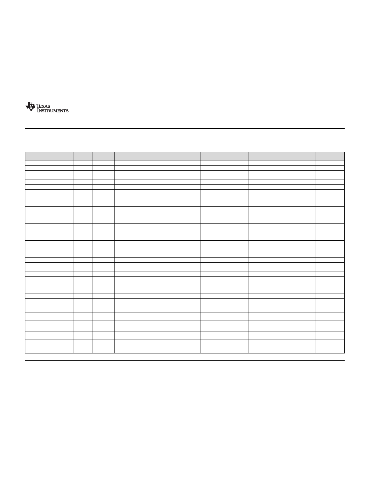
4.2 Bill of Materials
Table 3. BOM
Designator Quantity Value Description Package Reference Part Number Manufacturer
Alternate Part
Number
Alternate
Manufacturer
!PCB1 1 Printed Circuit Board HVL126 Any - C1, C2, C3 3 10µF CAP, TA, 10 µF, 25 V, ±10%, 0.3 Ω, SMD 6032-28 TPSC106K025R0300 AVX
C4, C5, C7, C9, C11 5 0.1µF
CAP, CERM, 0.1 µF, 50 V, ±10%, X7R,
0603
0603 C0603C104K5RACTU Kemet
C6 1 10µF CAP, TA, 10 µF, 50 V, ±10%, 0.3 Ω, SMD 7343-43 T495X106K050ATE300 Kemet
C8 1 1µF CAP, CERM, 1 µF, 25 V, ±10%, X5R, 0805 0805 08053D105KAT2A AVX
C12, C13 2 470pF
CAP, CERM, 470 pF, 50 V, ±5%,
C0G/NP0, 0603
0603 06035A471JAT2A AVX
C15, C16, C17, C18 4 1000pF
CAP, CERM, 1000 pF, 50 V, ±10%,
C0G/NP0, 0603
0603 06035A102KAT2A AVX
C19, C21 2 0.01µF
CAP, CERM, 0.01 µF, 25 V, ±5%,
C0G/NP0, 0603
0603 C0603H103J3GACTU Kemet
C24, C25 2 15pF
CAP, CERM, 15 pF, 50 V, ±5%, C0G/NP0,
0603
0603 C0603C150J5GACTU Kemet
C26 1 2200pF
CAP, CERM, 2200 pF, 25 V, ±10%, X7R,
0603
0603 GRM188R71E222KA01D MuRata
C27, C28 2 220pF
CAP, CERM, 220 pF, 50 V, ±5%,
C0G/NP0, 0603
0603 GRM1885C1H221JA01D MuRata
C29 1 0.47µF
CAP, CERM, 0.47 µF, 16 V, ±10%, X7R,
0603
0603 C0603C474K4RACTU Kemet
C30, C31, C33 3 0.1µF
CAP, CERM, 0.1 µF, 16 V, ±10%, X7R,
0603
0603 C0603C104K4RACTU Kemet
C32 1 1µF CAP, CERM, 1 µF, 16 V, ±10%, X7R, 0805 0805 C2012X7R1C105K TDK
C34 1 2.2µF
CAP, CERM, 2.2 µF, 10 V, ±10%, X7R,
0805
0805 C0805C225K8RACTU Kemet
C35 1 22µF CAP, AL, 22 µF, 10 V, ±20%, 1.35 Ω, SMD SMTRadial B EEE-FK1A220R Panasonic
C36 1 0.01µF
CAP, CERM, 0.01 µF, 16 V, ±10%, X7R,
0603
0603 GRM188R71C103KA01D MuRata
C37, C38 2 30pF
CAP, CERM, 30 pF, 50 V, ±5%, C0G/NP0,
0603
0603 GRM1885C1H300JA01D MuRata
D1 1 30V Diode, Schottky, 30 V, 1 A, SMA SMA B130L-13-F Diodes Inc.
D3, D12 2 Green LED, Green, SMD
LED,
2.3x1.4x1.5mm
LP M67K-D2G1-25-Z OSRAM
D4 1 Super Red LED, Super Red, SMD 2.2x1.3x1.4mm VLMS20J2L1-GS08 Vishay-Semiconductor
D5, D6, D9, D11 4 Yellow LED, Yellow, SMD
LED,
1.3x0.65x0.8mm
LY L29K-J1K2-26-Z OSRAM
D7 1 60V Diode, Schottky, 60V, 2A, SMB SMB MBRS260T3G ON Semiconductor
D8 1 20V Diode, Zener, 20V, 500 mW, SOD-123 SOD-123 MMSZ4707-V Vishay-Semiconductor
D10 1 5.6V Diode, Zener, 5.6 V, 5 W, SMB SMB SMBJ5339B-TP
Micro Commercial
Components
F1 1 Fuse, 1.5 A, 125 V, SMD SloBlo452 045201.5 Littelfuse
H1, H2, H3, H4 4
Machine Screw, Round, #4-40 x 1/4, Nylon,
Philips panhead
Screw NY PMS 440 0025 PH B&F Fastener Supply - -
Page 24
Schematics, Bill of Materials, and Layout
www.ti.com
24
SLAU658–March 2016
Submit Documentation Feedback
Copyright © 2016, Texas Instruments Incorporated
PGA411-Q1 EVM User's Guide
Table 3. BOM (continued)
Designator Quantity Value Description Package Reference Part Number Manufacturer
Alternate Part
Number
Alternate
Manufacturer
H5, H6, H7, H8 4 Standoff, Hex, 0.5"L #4-40 Nylon Standoff 1902C Keystone - J1 1 Header, 100mil, 2x1, Tin, TH
Header, 2x1,
100mil, TH
5-146278-2 TE Connectivity
J2 1 Header, 100mil, 3x1, Tin, TH
Header, 3x1,
100mil, TH
5-146278-3 TE Connectivity
J3, J5 2 Header, 100mil, 3x2, Tin, TH
Header, 100mil,
3x2, TH
5-146254-3 TE Connectivity
J4, J6, J7 3
Terminal Block, 6A, 3.5mm Pitch, 2-Pos,
TH
7.0x8.2x6.5mm ED555/2DS On-Shore Technology
J8, J10, J12 3 Header, 100mil, 7x2, Tin, TH
Header, 7x2,
100mil, Tin
PEC07DAAN Sullins Connector Solutions
J9 1 Connector, SMA Jack, Vertical, Gold, SMD SMA 142-0711-201 Emerson Network Power
J11 1 Header, 100mil, 15x2, Gold, TH 15x 2 Header MTSW-115-22-G-D-315 Samtec
J13 1 Header, 100mil, 6x1, Tin, TH
TH, 6-Leads, Body
608x100mil, Pitch
100mil
PEC06SAAN Sullins Connector Solutions
J14 1 Header, 100mil, 5x2, Tin, TH
Header, 5x2,
100mil, Tin
PEC05DAAN Sullins Connector Solutions
J15 1
Connector, Receptacle, Mini-USB Type B,
R/A, Top Mount SMT
USB Mini Type B 1734035-2 TE Connectivity
J17, J18, J19 3
Standard Banana Jack, Uninsulated,
5.5mm
Keystone_575-4 575-4 Keystone
L1 1 1000 Ω
Ferrite Bead, 1000 Ω at 100 MHz, 0.3 A,
0805
0805 BK2125HS102-T Taiyo Yuden
L2 1 56µH
Inductor, Shielded Drum Core, Ferrite,
56µH, 2A, 0.101 Ω, SMD
10x5x10mm 7447714560 Wurth Elektronik eiSos
L3 1 50 Ω Ferrite Bead, 50 Ω at 100MHz, 6A, 1206 1206 HI1206T500R-10 Laird-Signal Integrity Products
LBL1 1
Thermal Transfer Printable Labels, 0.650"
W x 0.200" H - 10,000 per roll
PCB Label 0.650"H
x 0.200"W
THT-14-423-10 Brady - -
Q1 1 30V MOSFET, N/P-CH, 30 V, 2.5 A, SSOT-6 SSOT-6 FDC6333C Fairchild Semiconductor None
R1, R13, R36, R76 4 0 RES, 0, 5%, 0.1 W, 0603 0603 RC0603JR-070RL Yageo America
R2, R11, R12 3 10.0k RES,10.0 k, 0.1%, 0.1 W, 0603 0603 RT0603BRD0710KL Yageo America
R3, R4, R5, R6, R7, R8, R45 7 1.2k RES, 1.2 k, 5%, 0.1 W, 0603 0603 RC0603JR-071K2L Yageo America
R9, R10 2 0 RES, 0, 5%, 0.333 W, 0805 0805 CRCW08050000Z0EAHP Vishay-Dale
R15, R33, R61, R65, R69 5 40.2k RES, 40.2 k, 0.1%, 0.1 W, 0603 0603 RT0603BRD0740K2L Yageo America
R16, R17 2 49.9k RES, 49.9 k, 1%, 0.1 W, 0603 0603 RC0603FR-0749K9L Yageo America
R18, R19, R20, R21, R25, R26,
R27, R28
8 30.0k RES, 30.0 k, 1%, 0.1 W, 0603 0603 RC0603FR-0730KL Yageo America
R29, R30 2 20.0k RES, 20.0 k, 0.1%, 0.1 W, 0603 0603 RT0603BRD0720KL Yageo America
R37, R38 2 10k RES, 10 k, 5%, 0.1 W, 0603 0603 RC0603JR-0710KL Yageo America
R44, R51, R52, R54, R55 5 4.7k RES, 4.7 k, 5%, 0.063 W, 0402 0402 CRCW04024K70JNED Vishay-Dale
R46, R47 2 33 RES, 33, 5%, 0.063 W, 0402 0402 CRCW040233R0JNED Vishay-Dale
R48 1 1.5k RES, 1.5 k, 5%, 0.063 W, 0402 0402 CRCW04021K50JNED Vishay-Dale
R49 1 100k RES, 100 k, 5%, 0.063 W, 0402 0402 CRCW0402100KJNED Vishay-Dale
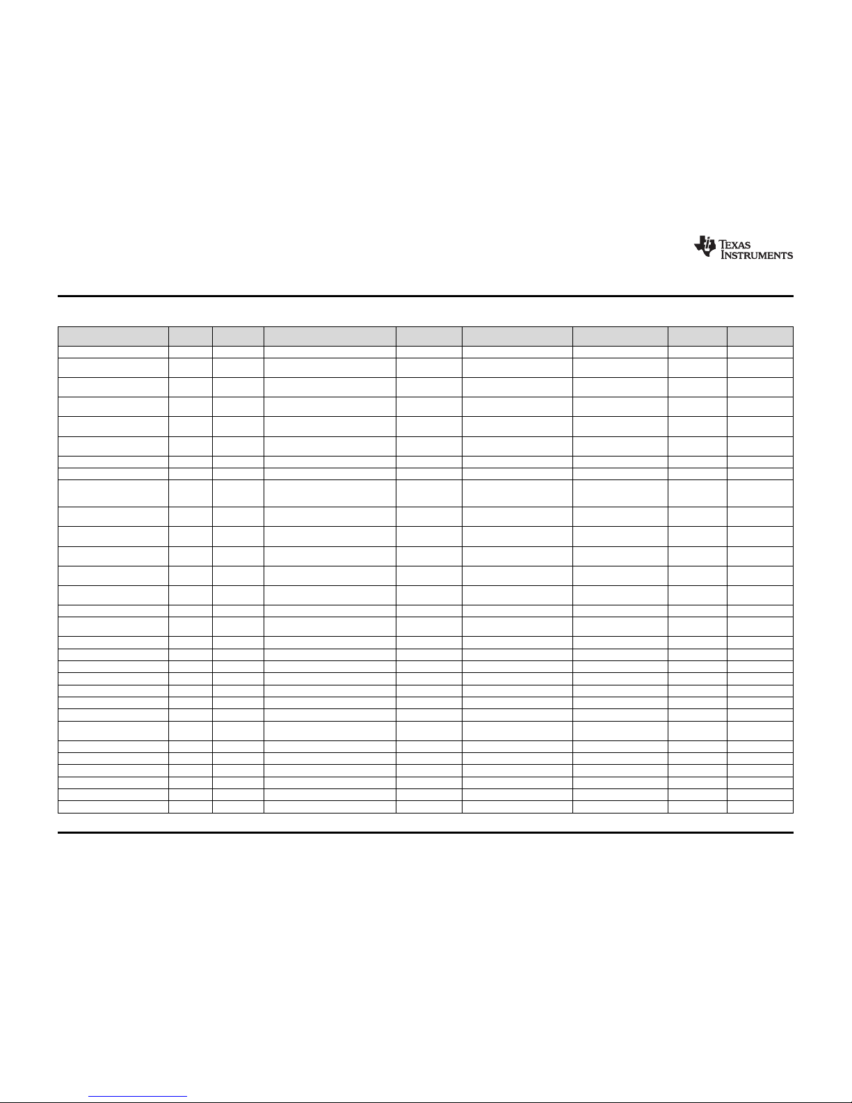
Page 25
www.ti.com
Schematics, Bill of Materials, and Layout
25
SLAU658–March 2016
Submit Documentation Feedback
Copyright © 2016, Texas Instruments Incorporated
PGA411-Q1 EVM User's Guide
Table 3. BOM (continued)
Designator Quantity Value Description Package Reference Part Number Manufacturer
Alternate Part
Number
Alternate
Manufacturer
R50 1 33k RES, 33 k, 5%, 0.063 W, 0402 0402 CRCW040233K0JNED Vishay-Dale
R53 1 1.2Meg RES, 1.2 M, 5%, 0.1 W, 0603 0603 CRCW06031M20JNEA Vishay-Dale
R56, R58, R60, R62, R64, R66,
R68, R70, R72, R74
10 200k RES, 200 k, 0.1%, 0.1 W, 0603 0603 RT0603BRD07200KL Yageo America
R57, R59, R63, R67, R71, R73,
R75
7 300k RES, 300 k, 0.1%, 0.1 W, 0603 0603 RG1608P-304-B-T5 Susumu Co Ltd
R78, R79 2 1.0k RES, 1.0 k, 5%, 0.1 W, 0603 0603 RC0603JR-071KL Yageo America
R80 1 0 RES, 0, 5%, 0.25 W, 1206 1206 RC1206JR-070RL Yageo America
S1 1 Switch, Slide, 4PDT,TH
Switch, 4P2T,
15x18x9.4 mm
1825264-1 TE Connectivity
S2, S3, S4 3 Switch, Tactile, SPST-NO, 0.1A, 16V, SMT 4.93x4.19x6.2 mm 7914G-1-000E Bourns
SH-J2, SH-J3, SH-J5, SH-J5 4 1x2 Shunt, 100mil, Gold plated, Black Shunt 969102-0000-DA 3M SNT-100-BK-G Samtec
TP65, TP66, TP67, TP85, TP86 5 Red Test Point, Miniature, Red, TH
Red Miniature
Testpoint
5000 Keystone
TP68, TP69, TP70, TP71, TP72,
TP73, TP74, TP75
8 Blue Test Point, Miniature, Blue, TH
Blue Miniature
Testpoint
5117 Keystone
TP76, TP77, TP78, TP79, TP80,
TP81, TP82, TP83, TP84
9 Black Test Point, Miniature, Black, TH
Black Miniature
Testpoint
5001 Keystone
U1 1
1-MHz, Micro-Power, Low-Noise, RRIO,1.8V CMOS OPERATIONAL AMPLIFIER
Precision Value Line Series, D0008A
D0008A OPA2313IDR Texas Instruments OPA2313ID Texas Instruments
U2 1
Dual 150mA, Low Iq LDO regulator,
DPQ0006A
DPQ0006A TLV7163318PDPQR Texas Instruments
TLV7163318PDP
QT
Texas Instruments
U3 1 PGA411PAP, PAP0064M PAP0064M PGA411PAP Texas Instruments None
U4, U5, U6, U7, U8 5
8-BIT DUAL-SUPPLY BUS TRANSCEIVER
with CONFIGURABLE VOLTAGE
TRANSLATION AND 3-STATE OUTPUT,
DGV0024A
DGV0024A SN74LVC8T245DGVR Texas Instruments TexasInstruments
U9 1 Mixed Signal MicroController, PN0080A PN0080A MSP430F5529IPN Texas Instruments None
U10 1
500mA, Low Quiescent Current, Ultra-Low
Noise, High PSRR Low-Dropout Linear
Regulator, DRB0008A
DRB0008A TPS73533DRB Texas Instruments None
Y1 1 Crystal, 20.000MHz, 8pF, SMD 3.2x0.75x2.5mm NX3225GA-20MHZ-STD-CRA-1 NDK
Y2 1 Crystal, 24.000MHz, 20pF, SMD
Crystal,
11.4x4.3x3.8mm
ECS-240-20-5PX-TR ECS Inc.
C10 0 0.01µF
CAP, CERM, 0.01 µF, 50 V, ±5%, X7R,
0805
0805 08055C103JAT2A AVX
C14, C20, C22, C23 0 51pF
CAP, CERM, 51 pF, 50 V, ±5%, C0G/NP0,
0603
0603 GRM1885C1H510JA01D MuRata
D2 0 5.1V Diode, Zener, 5.1 V, 500 mW, SOD-123 SOD-123 MMSZ5231B-7-F Diodes Inc.
FID1, FID2, FID3, FID4, FID5, FID6 0
Fiducial mark. There is nothing to buy or
mount.
N/A N/A N/A
R14 0 0 RES, 0, 5%, 0.333 W, 0805 0805 CRCW08050000Z0EAHP Vishay-Dale
R22, R23, R31, R32 0 100 RES, 100, 1%, 0.25 W, TH 1/4W Resistor CMF50100R00FHEB Vishay-Dale
R24, R34 0 4.99k RES, 4.99 k, 0.1%, 0.1 W, 0603 0603 RT0603BRD074K99L Yageo America
R35 0 50 RES,50, 1%, 0.1 W, 0603 0603 CRCW060350R0FKEA Vishay-Dale
Page 26

Schematics, Bill of Materials, and Layout
www.ti.com
26
SLAU658–March 2016
Submit Documentation Feedback
Copyright © 2016, Texas Instruments Incorporated
PGA411-Q1 EVM User's Guide
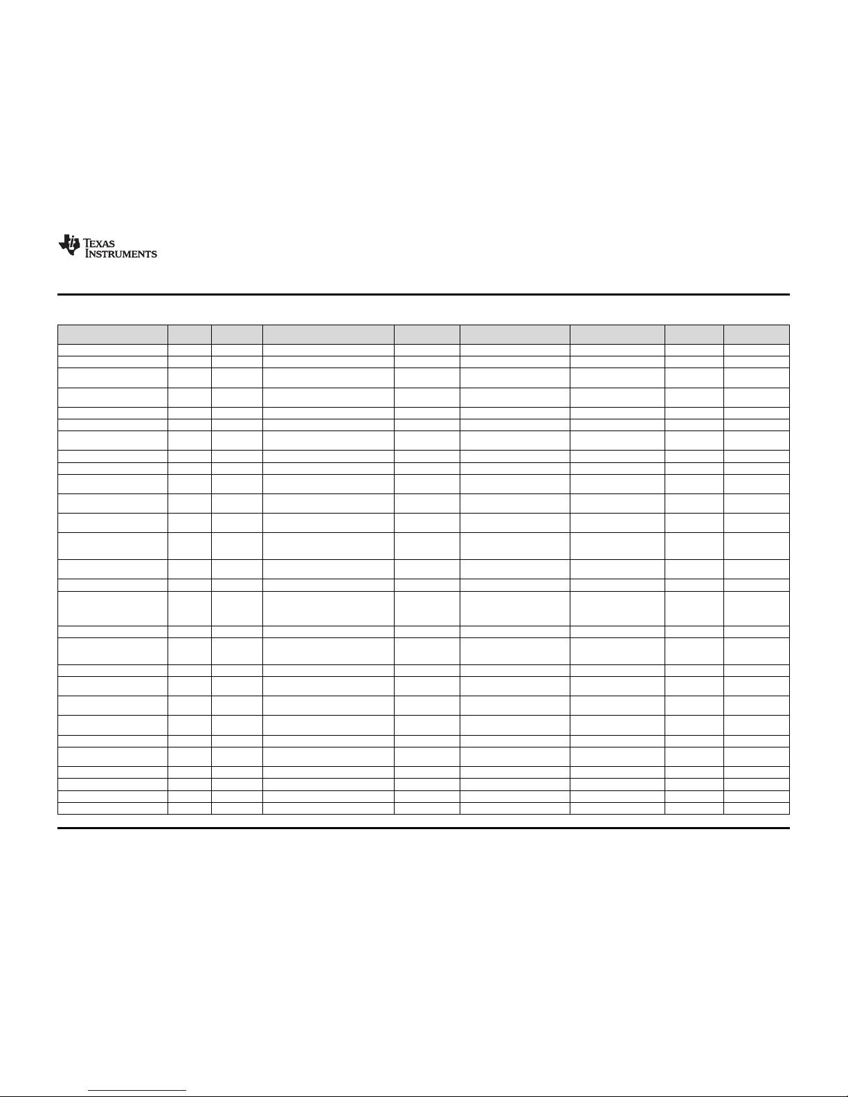
Table 3. BOM (continued)
Designator Quantity Value Description Package Reference Part Number Manufacturer
Alternate Part
Number
Alternate
Manufacturer
R39, R40, R41, R42, R43 0 33
RES, 33, 5%, 0.0625 W, Resistor Array 8x1
Resistor Array - 8x1 EXB-2HV330JV Panasonic
R77 0 0 RES, 0, 5%, 0.1 W, 0603 0603 RC0603JR-070RL Yageo America
TP1, TP2, TP3, TP4, TP5, TP6,
TP7, TP8, TP9, TP10, TP11, TP12,
TP13, TP14, TP15, TP16, TP17,
TP18, TP19, TP20, TP21, TP22,
TP23, TP24, TP25, TP26, TP27,
TP28, TP29, TP30, TP31, TP32,
TP33, TP34, TP35, TP36, TP37,
TP38, TP39, TP40, TP41, TP42,
TP43, TP44, TP45, TP46, TP47,
TP48, TP49, TP50, TP51, TP52,
TP53, TP54, TP55, TP56, TP57,
TP58, TP59, TP60, TP61, TP62,
TP63, TP64
0 Black Test Point, Miniature, Black, TH
Black Miniature
Testpoint
5001 Keystone
Page 27
www.ti.com
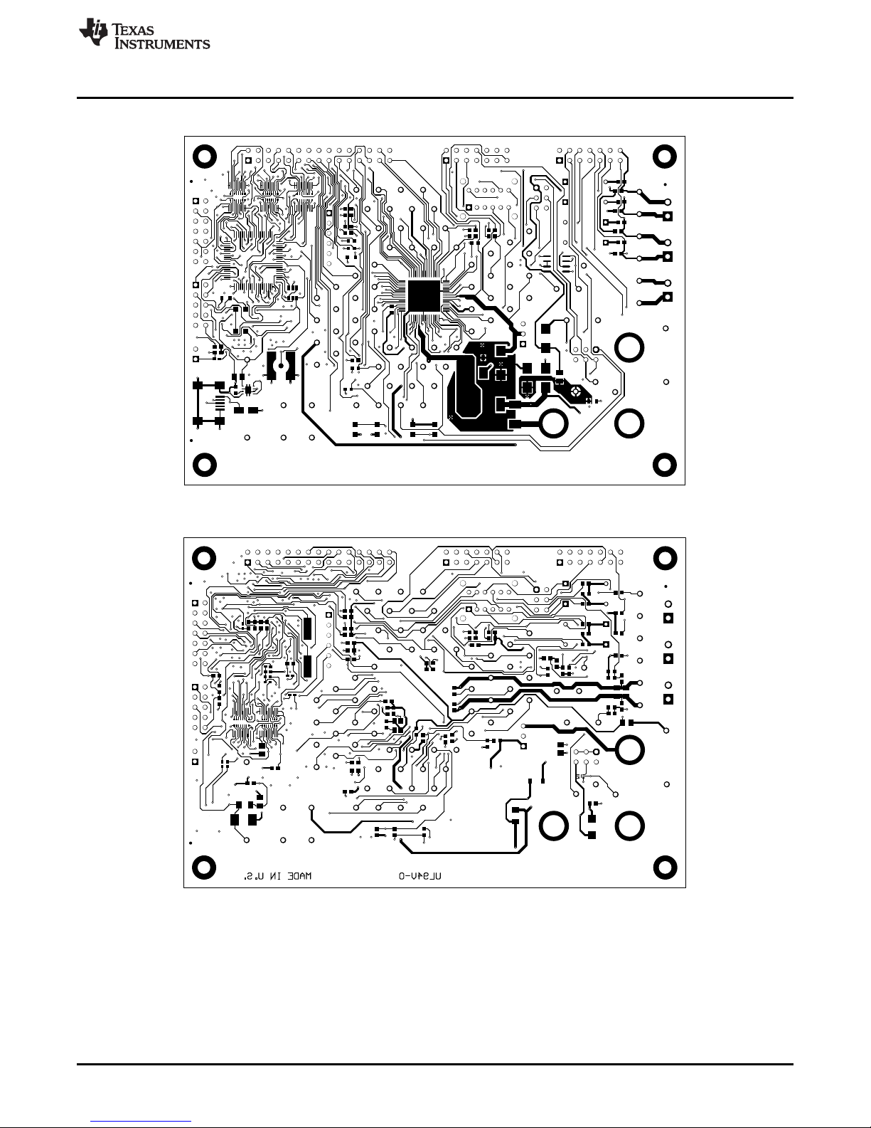
4.3 Layout and Component Placement
Schematics, Bill of Materials, and Layout
Figure 24. Top-Side Layout
Figure 25. Bottom-Side Layout
SLAU658–March 2016
Submit Documentation Feedback
Copyright © 2016, Texas Instruments Incorporated
PGA411-Q1 EVM User's Guide
27
Page 28

IMPORTANT NOTICE
Texas Instruments Incorporated and its subsidiaries (TI) reserve the right to make corrections, enhancements, improvements and other
changes to its semiconductor products and services per JESD46, latest issue, and to discontinue any product or service per JESD48, latest
issue. Buyers should obtain the latest relevant information before placing orders and should verify that such information is current and
complete. All semiconductor products (also referred to herein as “components”) are sold subject to TI’s terms and conditions of sale
supplied at the time of order acknowledgment.
TI warrants performance of its components to the specifications applicable at the time of sale, in accordance with the warranty in TI’s terms
and conditions of sale of semiconductor products. Testing and other quality control techniques are used to the extent TI deems necessary
to support this warranty. Except where mandated by applicable law, testing of all parameters of each component is not necessarily
performed.
TI assumes no liability for applications assistance or the design of Buyers’ products. Buyers are responsible for their products and
applications using TI components. To minimize the risks associated with Buyers’ products and applications, Buyers should provide
adequate design and operating safeguards.
TI does not warrant or represent that any license, either express or implied, is granted under any patent right, copyright, mask work right, or
other intellectual property right relating to any combination, machine, or process in which TI components or services are used. Information
published by TI regarding third-party products or services does not constitute a license to use such products or services or a warranty or
endorsement thereof. Use of such information may require a license from a third party under the patents or other intellectual property of the
third party, or a license from TI under the patents or other intellectual property of TI.
Reproduction of significant portions of TI information in TI data books or data sheets is permissible only if reproduction is without alteration
and is accompanied by all associated warranties, conditions, limitations, and notices. TI is not responsible or liable for such altered
documentation. Information of third parties may be subject to additional restrictions.
Resale of TI components or services with statements different from or beyond the parameters stated by TI for that component or service
voids all express and any implied warranties for the associated TI component or service and is an unfair and deceptive business practice.
TI is not responsible or liable for any such statements.
Buyer acknowledges and agrees that it is solely responsible for compliance with all legal, regulatory and safety-related requirements
concerning its products, and any use of TI components in its applications, notwithstanding any applications-related information or support
that may be provided by TI. Buyer represents and agrees that it has all the necessary expertise to create and implement safeguards which
anticipate dangerous consequences of failures, monitor failures and their consequences, lessen the likelihood of failures that might cause
harm and take appropriate remedial actions. Buyer will fully indemnify TI and its representatives against any damages arising out of the use
of any TI components in safety-critical applications.
In some cases, TI components may be promoted specifically to facilitate safety-related applications. With such components, TI’s goal is to
help enable customers to design and create their own end-product solutions that meet applicable functional safety standards and
requirements. Nonetheless, such components are subject to these terms.
No TI components are authorized for use in FDA Class III (or similar life-critical medical equipment) unless authorized officers of the parties
have executed a special agreement specifically governing such use.
Only those TI components which TI has specifically designated as military grade or “enhanced plastic” are designed and intended for use in
military/aerospace applications or environments. Buyer acknowledges and agrees that any military or aerospace use of TI components
which have not been so designated is solely at the Buyer's risk, and that Buyer is solely responsible for compliance with all legal and
regulatory requirements in connection with such use.
TI has specifically designated certain components as meeting ISO/TS16949 requirements, mainly for automotive use. In any case of use of
non-designated products, TI will not be responsible for any failure to meet ISO/TS16949.
Products Applications
Audio www.ti.com/audio Automotive and Transportation www.ti.com/automotive
Amplifiers amplifier.ti.com Communications and Telecom www.ti.com/communications
Data Converters dataconverter.ti.com Computers and Peripherals www.ti.com/computers
DLP® Products www.dlp.com Consumer Electronics www.ti.com/consumer-apps
DSP dsp.ti.com Energy and Lighting www.ti.com/energy
Clocks and Timers www.ti.com/clocks Industrial www.ti.com/industrial
Interface interface.ti.com Medical www.ti.com/medical
Logic logic.ti.com Security www.ti.com/security
Power Mgmt power.ti.com Space, Avionics and Defense www.ti.com/space-avionics-defense
Microcontrollers microcontroller.ti.com Video and Imaging www.ti.com/video
RFID www.ti-rfid.com
OMAP Applications Processors www.ti.com/omap TI E2E Community e2e.ti.com
Wireless Connectivity www.ti.com/wirelessconnectivity
Mailing Address: Texas Instruments, Post Office Box 655303, Dallas, Texas 75265
Copyright © 2016, Texas Instruments Incorporated
Page 29

Mouser Electronics
Authorized Distributor
Click to View Pricing, Inventory, Delivery & Lifecycle Information:
Texas Instruments:
PGA411Q1EVM
 Loading...