

Page 1

User's Guide
SBOU084–February 2010
PGA309EVM-USB
This user’s guide describes the characteristics, operation, and use of the PGA309EVM-USB evaluation
module (EVM). This EVM is designed to evaluate the performance of the PGA309, a voltage output,
programmable sensor conditioner. This document covers all pertinent areas involved to properly use this
EVM board, allowing for user evaluation suitable to a variety of applications. This document also includes
the physical printed circuit board (PCB) layout and circuit descriptions. A schematic of the
PGA309EVM-USB is available as a separate download from the TI web site.
Contents
1 Introduction and Overview ................................................................................................. 2
2 System Setup ................................................................................................................ 5
3 PGA309EVM-USB Hardware Setup .................................................................................... 16
4 PGA309EVM-USB Software Overview ................................................................................. 25
List of Figures
1 Hardware Included with the INA282-286EVM........................................................................... 3
2 PGA309EVM-USB Hardware Setup...................................................................................... 5
3 PGA309_Test_Board Block Diagram .................................................................................... 5
4 PGA309_Test_Board Schematic: Input Circuitry ....................................................................... 7
5 PGA309_Test_Board Schematic: Power, Reference, and Digital Connections.................................... 8
6 PGA309_Test_Board Schematic: Output Circuitry..................................................................... 9
7 PGA309_Test_Board Schematic: Sensor Emulator Circuitry........................................................ 10
8 PGA309_Test_Board Connections to USB-DAQ-Platform and EEPROM......................................... 11
9 Theory of Operation For USB-DAQ-Platform.......................................................................... 16
10 PGA309EVM-USB Typical Hardware Connections................................................................... 17
11 Connecting the Two EVM PCBs ........................................................................................ 18
12 Connecting Power to the EVM........................................................................................... 19
13 Connecting the USB Cable............................................................................................... 20
14 Default Jumper Settings (PGA309_Test_Board)...................................................................... 21
15 Default Jumper Settings (USB-DAQ-Platform) ........................................................................ 22
16 PGA309EVM-USB Software: Registers Tab........................................................................... 26
17 PGA309EVM-USB Software: EEPROM Tab .......................................................................... 27
18 PGA309EVM-USB Software: Block Diagram.......................................................................... 28
19 PGA309EVM-USB Software: Auto Calibrate Tab—Sensor Definition.............................................. 29
20 PGA309EVM-USB Software: Sensor Emulator Control Panel Tool................................................ 30
21 PGA309EVM-USB Software: Auto Calibrate Tab—PGA Setup..................................................... 31
22 PGA309EVM-USB Software: Auto Calibrate Tab—Two-Point Calibration and Linearization................... 32
23 PGA309EVM-USB Software: Auto Calibrate Tab—Temperature Error Compensation.......................... 33
24 PGA309EVM-USB Software: Auto Calibrate Tab—Post Cal Error Check......................................... 34
25 PGA309EVM-USB Software: Auto Calibrate Tab—DMM Options.................................................. 35
Microsoft, Windows are registered trademarks of Microsoft Corporation.
I2C is a trademark of NXP Semiconductors.
All other trademarks are the property of their respective owners.
SBOU084–February 2010 PGA309EVM-USB
Submit Documentation Feedback
Copyright © 2010, Texas Instruments Incorporated
1
Page 2

Introduction and Overview
1 PGA309 Test Board Parts List........................................................................................... 12
2 J1 Pinout (25-Pin Male DSUB) .......................................................................................... 14
3 J2 Pinout (25-Pin Female DSUB) ...................................................................................... 15
4 PGA309_Test_Board Jumper Functions: General.................................................................... 22
5 PGA309_Test_Board Jumper Functions: Miscellaneous Connections............................................. 23
6 PGA309_Test_Board Jumper Functions: Sensor Emulator Section ............................................... 23
7 USB-DAQ-Platform Jumper Settings ................................................................................... 24
1 Introduction and Overview
This document provides the information needed to set up and operate the PGA309EVM-USB evaluation
module, a test platform for the PGA309 programmable sensor conditioner. For a more detailed description
of the PGA309, refer to the product data sheet (SBOS292) available from the Texas Instruments web site
at http://www.ti.com. Additional support documents are listed in the section of this guide entitled Related
Documentation from Texas Instruments.
The PGA309EVM-USB is an evaluation module that is used to fully evaluate the PGA309. The PGA309 is
an integrated circuit that provides temperature compensation and linearization for bridge sensors. The
PGA309EVM-USB consists of two PCBs. One board (the USB-DAQ-Platform) generates the digital
signals required to communicate with the PGA309. The other board (the PGA309_Test_Board) contains
the PGA309 device, as well as support and configuration circuitry.
Throughout this document, the abbreviation EVM and the term evaluation module are synonymous with
the PGA309EVM-USB.
www.ti.com
List of Tables
2
PGA309EVM-USB SBOU084–February 2010
Copyright © 2010, Texas Instruments Incorporated
Submit Documentation Feedback
Page 3
www.ti.com
1.1 PGA309EVM-USB Hardware
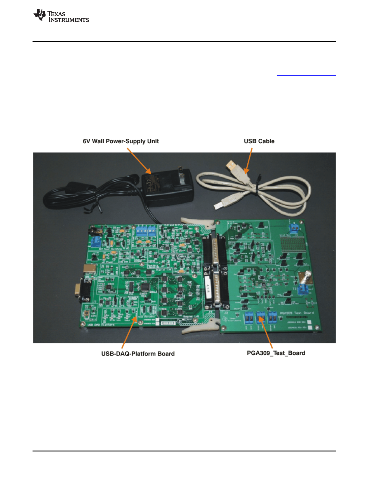
Figure 1 shows the hardware included with the PGA309EVM-USB kit. Contact the factory if any
component is missing. It is highly recommended that you check the TI web site (at http://www.ti.com) to
verify that you have the latest software. It is also recommended that you refer to the PGA309 User's Guide
if you have questions about the PGA309 device itself.
The complete kit includes the following items:
• PGA309_Test_Board
• USB DAQ Platform Board
• USB cable
• 6V wall power-supply unit
• CD-ROM containing this user's guide and product software
Introduction and Overview
Figure 1. Hardware Included with the INA282-286EVM
SBOU084–February 2010 PGA309EVM-USB
Submit Documentation Feedback
Copyright © 2010, Texas Instruments Incorporated
3
Page 4
Introduction and Overview
1.2 Related Documentation from Texas Instruments
The following documents provides information regarding Texas Instruments integrated circuits used in the
assembly of the PGA309EVM-USB. This user's guide is available from the TI web site under literature
number SBOU084. Any letter appended to the literature number corresponds to the document revision
that is current at the time of the writing of this document. Newer revisions may be available from the TI
web site at http://www.ti.com, or call the Texas Instruments Literature Response Center at (800) 477-8924
or the Product Information Center at (972) 644-5580. When ordering, identify the document by both title
and literature number.
Document Literature Number
PGA309 SBOS292
USB DAQ Platform Users Guide SBOU056
PGA309 Users Guide SBOU024
OPA333 Product Data Sheet SBOS351
DAC8555 Product Data Sheet SLAS475
XTR117 Product Data Sheet SBOS344
PGA309EVM-USB Schematic SBOR010
Sensor-Emulator EVM Reference Guide SBOA102
1.3 If You Need Assistance
If you have questions about the PGA309EVM-USB evaluation module, send an e-mail to the Linear
Application Team at precisionamps@list.ti.com. Include PGA309EVM-USB as the subject heading.
www.ti.com
1.4 Information About Cautions and Warnings
This document contains caution statements.
This is an example of a caution statement. A caution statement describes a
situation that could potentially damage your software or equipment.
CAUTION
4
PGA309EVM-USB SBOU084–February 2010
Copyright © 2010, Texas Instruments Incorporated
Submit Documentation Feedback
Page 5
USBDAQ
Platform
PGA309
TestBoard
EVM
Power
PGA309
V Supply
Switched5.0VPower
DUT
One-WireInterface
25-Pin
MaleDSUBSignals
FromUSBDAQPlatform
25-Pin
FemaleDSUBSignals
FromUSBDAQPlatform
I C
Interface
2
4mAto20mA
I/VConverter
Sensor
Connection
Sensor
Emulator
www.ti.com
2 System Setup
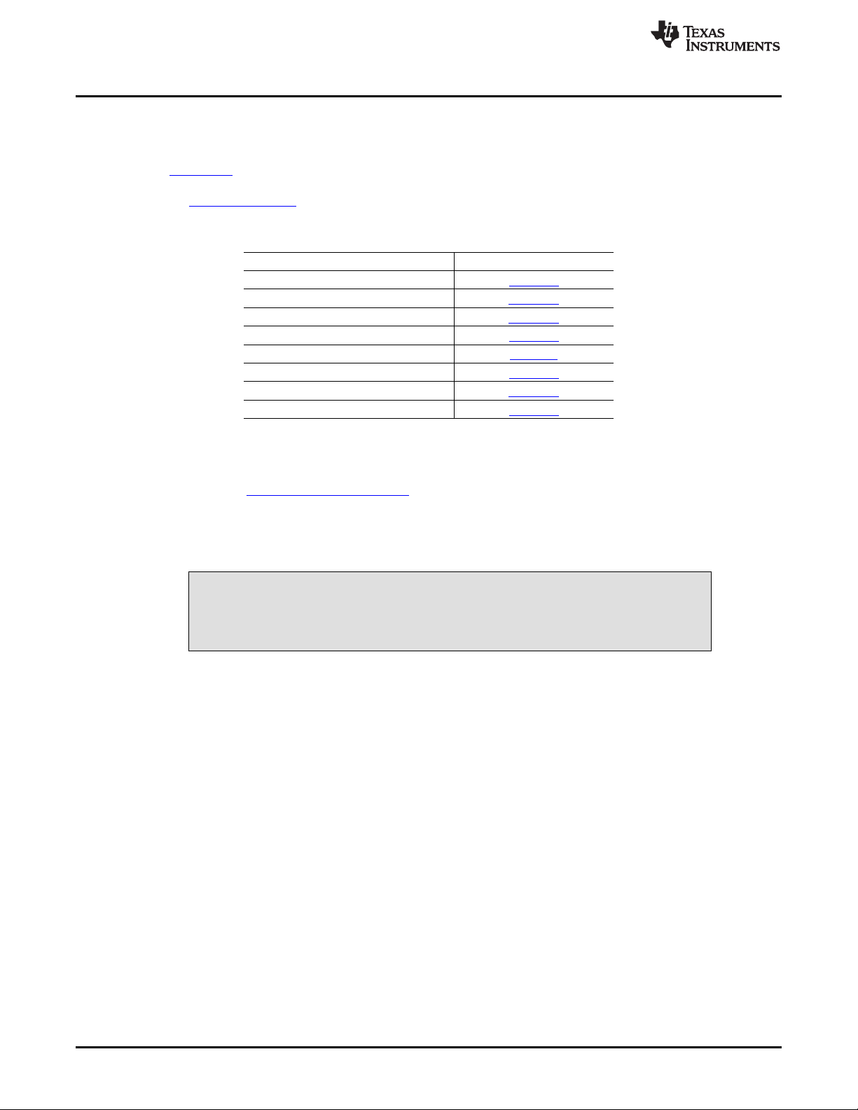
Figure 2 shows the system setup for the PGA309EVM. The PC runs software that communicates with the
USB-DAQ-Platform. The USB-DAQ-Platform generates the digital signals used to communicate with the
PGA309_Test_Board. Connectors on the PGA309_Test_Board allow for connection to the bridge sensor.
System Setup
2.1 Theory of Operation for PGA309_Test_Board Hardware
Figure 2. PGA309EVM-USB Hardware Setup
Figure 3 shows the block diagram of the PGA309_Test_Board. The PGA309_Test_Board provides
connections to the I2C™, one-wire, analog-to-digital converters (ADCs) and digital-to-analog converters
(DACs) on the USB-DAQ-Platform. It also provides connection points for external connection of the bridge
sensor. The PGA309_Test_Board has circuitry to convert the PGA309 voltage output to 4mA to 20mA
current.
SBOU084–February 2010 PGA309EVM-USB
Submit Documentation Feedback
Figure 3. PGA309_Test_Board Block Diagram
5
Copyright © 2010, Texas Instruments Incorporated
Page 6

System Setup
The PGA309_Test_Board also has an onboard sensor emulator. The sensor emulator is a circuit that
generates the same type of signals generated by a bridge sensor. The sensor emulator circuit is controlled
by the PGA309EVM-USB software. Using the sensor emulator allows you to get a deeper understanding
of the PGA309EVM-USB software and hardware more quickly. When the capabilities and functions of the
PGA309EVM-USB are fully understood, you can connect the real-world sensor to the EVM and perform a
full calibration.
Note that calibrations with real-world sensors are time-consuming because devices such as these are
normally calibrated at multiple temperatures in an environmental chamber. It is not unusual for
temperature calibration to require 12 hours.
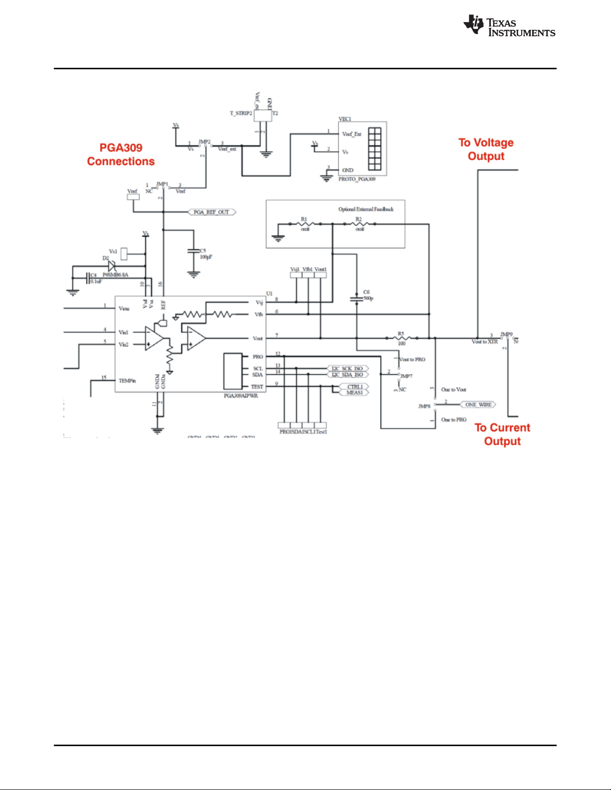
2.2 PGA309_Test_Board Connections
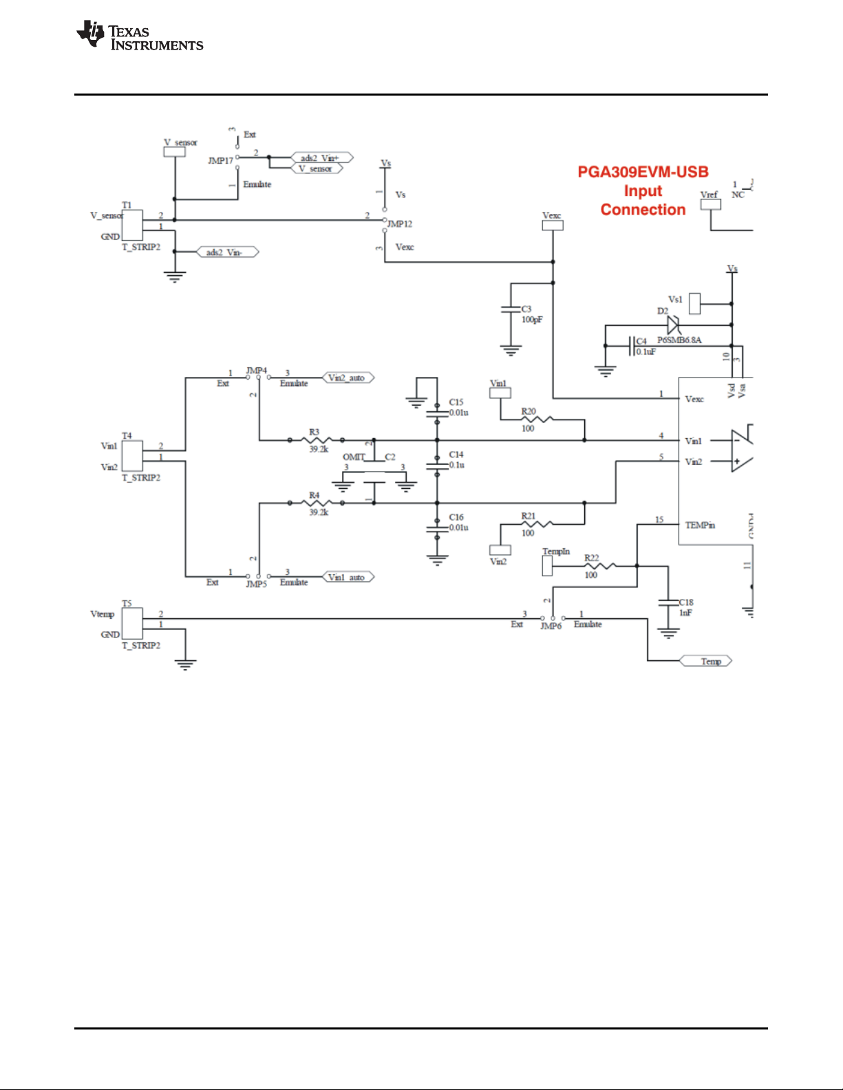
See Figure 4 for the input connections on the PGA309_Test_Board schematic. T1 provides the power
connection for an external bridge sensor. T4 allows connections to each input of the external bridge
sensor. T5 allows connection of the external temperature sensor. JMP7, JMP4, JMP5, and JMP6 allow
users to select either the onboard sensor emulator or an external sensor. JMP12 allows users to choose
between VSor V
The input is filtered with R3, R4, C14, C15, and C16. Note that C14 is ten times larger then C15, and C16
is used for good ac common-mode rejection. The cutoff frequency of this filter is 40.6Hz (f = 1/(2 p R3
C14)). This input filter is recommended in your final design if you have available board space.
V
has a 100pF capacitor and TEMPin has a 1nF capacitor. These components are also recommended
EXC
in your final design.
Refer to Figure 5 to see the power, reference, and digital connections on the PGA309_Test_Board
schematic. T2 provides a connection for an external reference voltage. JMP1 and JMP2 allow users to
select between the internal reference, an external reference, or power-supply reference. JMP7 and JMP8
allows users to connect the One-Wire signal to the PRG pin directly or through V
D2 is a transient voltage suppressor. It is useful in helping to prevent damage in an electrical overstress
(EOS) condition. R5 is useful in preventing EOS damage to the output. C6 filters noise at the output. C5
filters the reference output. These components are recommended for your design if PCB space permits.
C4 is a decoupling capacitor; it is required in the final design.
for the sensor power.
EXC
OUT
www.ti.com
.
6
PGA309EVM-USB SBOU084–February 2010
Copyright © 2010, Texas Instruments Incorporated
Submit Documentation Feedback
Page 7
www.ti.com
System Setup
Figure 4. PGA309_Test_Board Schematic: Input Circuitry
SBOU084–February 2010 PGA309EVM-USB
Submit Documentation Feedback
Copyright © 2010, Texas Instruments Incorporated
7
Page 8
System Setup
www.ti.com
Figure 5. PGA309_Test_Board Schematic: Power, Reference, and Digital Connections
8
PGA309EVM-USB SBOU084–February 2010
Copyright © 2010, Texas Instruments Incorporated
Submit Documentation Feedback
Page 9

www.ti.com
Figure 6 shows the output section of the PGA309EVM_Test_Board. There are two output options: voltage
output and current output. The voltage output option is selected by placing JMP9 in the NC position. The
current output option is selected by moving JMP9 to the V
to XTR position.
OUT
System Setup
Figure 6. PGA309_Test_Board Schematic: Output Circuitry
In voltage output mode, C10 = 10nF is connected to the PGA309 output. This capacitor is used for radio
frequency interference (RFI) and electromagnetic interference (EMI) immunity. This component should be
included in your design, if possible.
In current output mode, the PGA309 output is connected to a voltage-to-current (V-I) converter (XTR117).
The sum of R6 and R8 convert the output voltage from the PGA309 to an input current for the XTR117.
R7 can be used to create an input offset current using the reference. The total input current is IIN= V
(R6 + R8) + V
/R7. The output current is equal to the input current times the current gain (x 100).
REF
D4 is used for reverse polarity protection. D3 is used for over-voltage transient protection. D3 was
selected for low leakage. Leakage on D3 directly contributes to error. C11 is a decoupling capacitor and is
required for proper operation. The external transistor, Q1, conducts the majority of the full-scale output
current. Power dissipation in this transistor can approach 0.8W with high loop voltage (40V) and 20mA
output current.
SBOU084–February 2010 PGA309EVM-USB
Submit Documentation Feedback
Copyright © 2010, Texas Instruments Incorporated
OUT
/
9
Page 10
System Setup
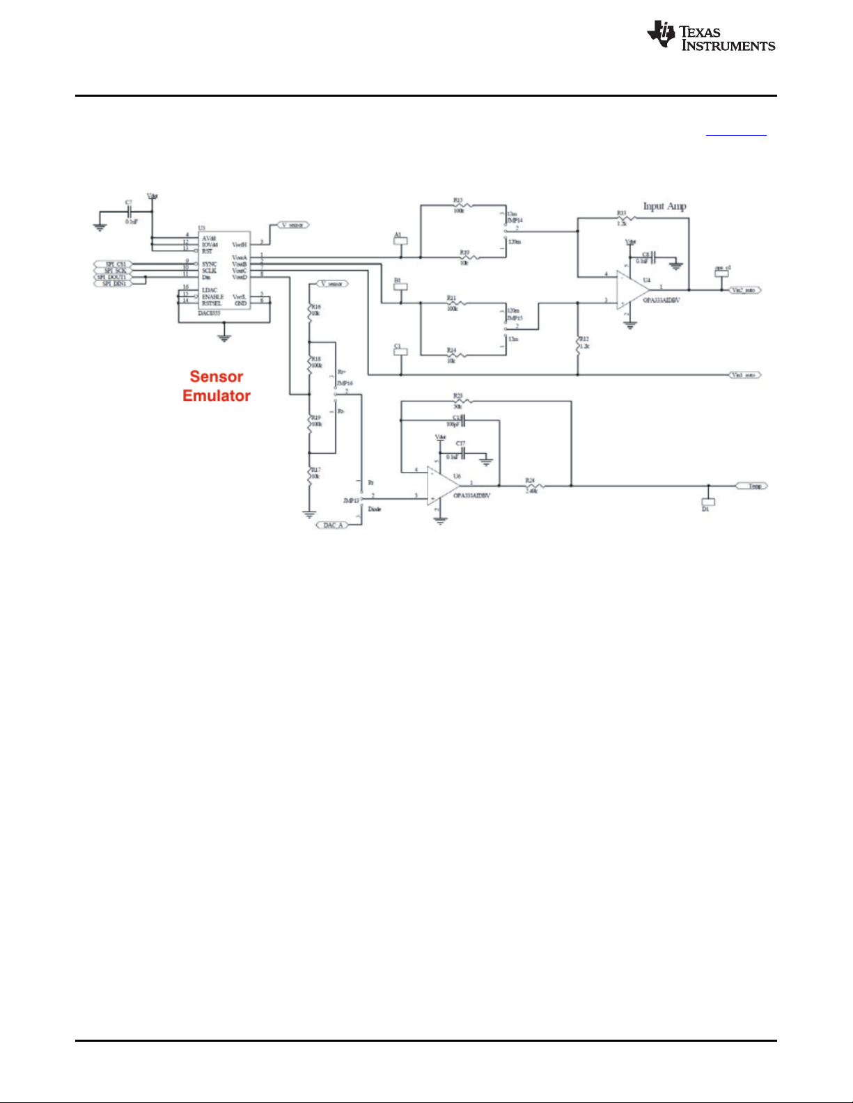
Figure 7 shows the sensor emulator circuit. The sensor emulator generates signals to help users evaluate
the PGA309. No part of this circuit is required in your final design. The sensor emulator uses a DAC8555
(U8) to generate an emulated temperature signal, common-mode signal, and differential signal. These
signals can be controlled using software to produce levels that closely match real-world sensors.
www.ti.com
Figure 7. PGA309_Test_Board Schematic: Sensor Emulator Circuitry
The operational amplifier U4 and associated resistors is a differential amplifier with jumper selectable
attenuation. The possible attenuations are 0.12 and 0.012. The attenuation produces a more accurate and
stable emulated sensor output. For example, when the DAC outputs 3V, the sensor emulator outputs 3V ×
0.012 = 36mV (assuming that attenuation is set in the 0.012 position). Thus, the maximum output of the
sensor emulator is 120mV/V and 12mV/V.
The op amp U6 buffers the emulated temperature signal. Resistors R16, R17, R18, and R19 are used to
attenuate the DAC output for temperature emulation and to reference the temperature signal to supply or
ground. JMP13 allows the resistor network to be bypassed for direct connection to the DAC (diode
temperature sensor mode).
10
PGA309EVM-USB SBOU084–February 2010
Submit Documentation Feedback
Copyright © 2010, Texas Instruments Incorporated
Page 11
www.ti.com
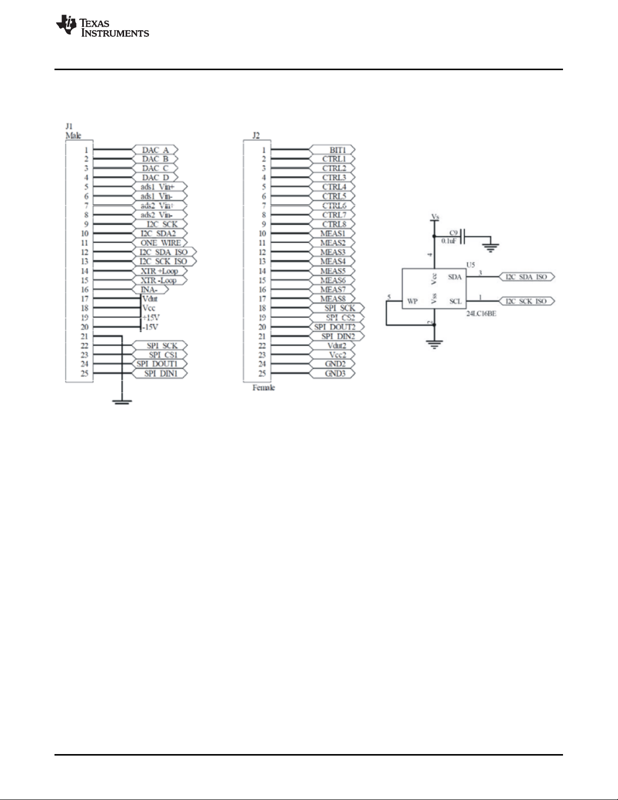
Figure 8 illustrates the two 25-pin D-SUB connectors J1 and J2. These connectors provide all the signals
necessary to communicate with the PGA309. U5 is the EEPROM used to store the calibration look-up
table used with the PGA309.
System Setup
Figure 8. PGA309_Test_Board Connections to USB-DAQ-Platform and EEPROM
SBOU084–February 2010 PGA309EVM-USB
Submit Documentation Feedback
Copyright © 2010, Texas Instruments Incorporated
11
Page 12

System Setup
2.3 PGA309_Test_Board Parts List
Table 1 describes the parts list for the PGA309_Test_Board.
Table 1. PGA309 Test Board Parts List
Qty Value Ref Des Description Vendor Part Number
1 560pF C6 Panasonic - ECG ECJ-1VC1H561J
3 100pF C3 C5, C13 ECJ-1VC2A101J
6 0.1µF C4, C7, C8, C9, C14, C17 Kemet CC0603ZRY5V8BB104
2 .01µF C15, C16 AVX 06031C103KAT2A
1 1nF C18 Panasonic - ECG ECJ-1VB2A102K
2 10nF C10, C11 Kemet C0603C103K5RACTU
1 0.02µF C12 TDK Corporation C1608X7R2A223K
1 1000pF C2 Omit; not installed JOHANSON DIELECTRICS 501R18W102KV4E
4 100kΩ R11, R15, R18, R19 Susumu Co Ltd RGH1608-2C-P-104-B
2 1.2kΩ R12, R13 Susumu Co Ltd RGH1608-2C-P-122-B
5 10kΩ R8, R10, R14, R16, R17 Susumu Co Ltd RGH1608-2C-P-103-B
4 100Ω R5, R20, R21, R22 Yageo Corporation RC0603FR-07100RL
1 191kΩ R7 Yageo Corporation ERJ-3EKF1913V
1 11.3kΩ R6 Yageo Corporation ERJ-3EKF1132V
2 39.2kΩ R3, R4 Yageo Corporation RC0603FR-0739K2L
1 50kΩ R23 Sunsuma RR0816P-4992-D-68C
1 2.49kΩ R24 Sunsuma RR0816P-2491-D-39H
0 omit R1, R2, R9 Omit; not installed
1 PGA309 U1 Smart Programmable Sensor Texas Instruments PGA309AIPWT
1 BNC P1 Tyco Electronics/Amp 5227699-1
OPA333AID
2 U4 U6 IC Op Amp 1.8V 0-DRIFT SOT23-5 Texas Instruments OPA333AIDBVT
1 DAC8555 U3 IC DAC 16BIT QUAD 16-TSSOP Texas Instruments DAC8555IPW
1 24LC16BT U5 Microchip Technology 24LC16BT-I/OT
1 XTR117 U2 Texas Instruments XTR117AIDGKT
1 D2 ON Semiconductor P6SMB6.8AT3G
1 SMAJ43A D3 TVS 400W 43V Unidirectional SMA SMAJ43A-TP
1 BAS70TP D4 BAS70TPMSCT-ND
1 NPN Q1 Fairchild Semiconductor BCP55
5 ED300/2 T1, T2, T3, T4, T5 On-Shore Technology Inc ED300/2
BVT
6.8V TVS Zener Unidirectional 600W
transzorb 6.8V SMB
Capacitor, ceramic 560pF 50V NP0
0603
Capacitor, ceramic 560pF 50V NP0
0603
Capacitor, 0.1µF 25V, ceramic Y5V
0603
Capacitor, ceramic .01µF 10%
100V X7R 0603
Capacitor, 1000pF, 100V, ceramic
X7R 0603
Capacitor, 10000pF, 50V, ceramic
X7R 0603
Capacitor, ceramic 22000pF, 100V
X7R 10%0603
Resistor, 100kΩ 1/6W 0.1% 0603
SMD
Resistor, 1.2kΩ 1/6W 0.1% 0603
SMD
Resistor, 10.0kΩ 1/6W 0.1% 0603
SMD
Resistor, 100kΩ 1/10W 1% 0603
SMD
Resistor, 191kΩ 1/10W 1% 0603
SMD
Resistor, 11.3kΩ 1/10W 1% 0603
SMD
Resistor, 39.2kΩ 1/10W 1% 0603
SMD
Resistor, 49.9kΩ 1/16W .5% 0603
SMD
Resistor, 2.49kΩ 1/16W .5% 0603
SMD
Connector, Jack BNC Vertical 50Ω
PCB
IC SRL EEPROM 16K 2.5V
SOT23-5
IC 4mA-20mA Current-Loop TX
8-MSOP
Micro Commercial
Components
Diode, Schottky 70V 200mA Micro Commercial
SOT23 Components
IC, Transistor NPN SS GP 1.5A
SOT223-4
2-Position Terminal Strip, Cage
Clamp, 45º, 15A, Dove-tailed
www.ti.com
12
PGA309EVM-USB SBOU084–February 2010
Submit Documentation Feedback
Copyright © 2010, Texas Instruments Incorporated
Page 13

www.ti.com
System Setup
Table 1. PGA309 Test Board Parts List (continued)
Qty Value Ref Des Description Vendor Part Number
JMP1, JMP2, JMP3, JMP4,
JUMP2 Cut Terminal strip, 3-position, .100
17 JMP9, JMP10, JMP11, Samtec TSW-103-07-G-S
24 V
17 JMP9, JMP10, JMP11, Tyco Electronics Amp 881545-2
to Size centers, .025 square pins
TP Cut to Terminal strip, 1-position, .100
Size centers, .025 square pins
Jumper Shunt LP w/Handle 2-position,
Shunts 30AU
1 DSUB25M J1 25POS 30GOLD (with Threaded AMP/Tyco Electronics 5747842-4
1 DSUB25F J2 25POS 30GOLD (with Threaded AMP/Tyco Electronics 5747846-4
4 Standoffs 0.500" length, 0.250" OD, Keystone 2203
4 Screws Building Fasteners PMS 440 0038 PH
JMP5, JMP6, JMP7, JMP8,
JMP12, JMP13, JMP14,
JMP15, JMP16, JMP17,
V_Sensor, OPA_O1, C1,
B1, A,1 TempIn, GND1, D1,
GND2, V
OUT
V
1, VFB1, VS1, SCL1,
OUT
VSJ1, GND4, VIN1, SDA1,
GND3, Test1,
JMP1, JMP2, JMP3, JMP4,
JMP5, JMP6, JMP7, JMP8,
JMP12, JMP13, JMP14,
JMP15, JMP16, JMP17,
, V
,
EXC
_F1, VIN2, PRG1, Samtec TSW-101-07-G-S
REF
Connector, D-SUB PLUG R/A
Inserts and Board locks)
Connector, D-SUB RCPT R/A
Inserts and Board locks)
Standoffs, Hex , 4-40 Threaded,
Aluminum Iridite Finish
Machine Screw, 4-40x3/8" Phillips
PanHead, Steel, Zinc Plated
SBOU084–February 2010 PGA309EVM-USB
Submit Documentation Feedback
Copyright © 2010, Texas Instruments Incorporated
13
Page 14

System Setup
2.4 PGA309_Test_Board: Signal Definitions and Pinouts
This section provides the signal definitions for the PGA309_Test_Board.
2.4.1 J1 (25-Pin Male DSUB)
Table 2 shows the different signals connected to J1 on the PGA309_Test_Board. This table also identifies
signals connected to pins on J1 that are not used on the PGA309_Test_Board.
Table 2. J1 Pinout (25-Pin Male DSUB)
Pin on J1 Signal Used on This EVM PGA309 Pin
1 DAC A No
2 DAC B No
3 DAC C No
4 DAC D No
5 ADS1+ No
6 ADS1- No
7 ADS2+ No
8 ADS2– No
9 I2C_SCK No
10 I2C_SDA2 No
11 ONE_WIRE No
12 I2C_SCK_ISO Yes SCL
13 I2C_SDA_ISO Yes SDA
14 XTR_LOOP+ No
15 XTR_LOOP– No
16 INA– No
17 V
18 V
19 +15v No
20 –15v No
21 GND Yes GND
22 SPI_SCK No
23 SPI_CS1 No
24 SPI_DOUT No
25 SPI_DIN1 No
DUT
CC
Yes V
No
www.ti.com
S
14
PGA309EVM-USB SBOU084–February 2010
Submit Documentation Feedback
Copyright © 2010, Texas Instruments Incorporated
Page 15

www.ti.com
2.4.2 J2 (25-Pin Female DSUB)
Table 3 shows the different signals connected to J2 on the PGA309_Test_Board. This table also identifies
signals connected to pins on J2 that are not used on PGA309_Test_Board.
Pin on J2 Signal Used on This EVM PGA309 Pin
1 NC No
2 CTRL1 Yes Convert
3 CTRL2 Yes GPIO
4 CTRL3 No
5 CTRL4 No
6 CTRL5 No
7 CTRL6 No
8 CTRL7 No
9 CTRL8 No
10 MEAS1 Yes Warning
11 MEAS2 Yes GPIO
12 MEAS3 Yes Overlimit
13 MEAS4 Yes Critical
14 MEAS5 Yes ALT
15 MEAS6 No
16 MEAS7 No
17 MEAS8 No
18 SPI_SCK No
19 SPI_CS2 No
20 SPI_DOUT2 No
21 SPI_DIN2 No
22 V
23 V
24 GND Yes GND
25 GND Yes GND
Table 3. J2 Pinout (25-Pin Female DSUB)
DUT
CC
No V
No
System Setup
S
SBOU084–February 2010 PGA309EVM-USB
Submit Documentation Feedback
Copyright © 2010, Texas Instruments Incorporated
15
Page 16

TUSB3210
8052 C
withUSBInterface
andUART
m
USBBus
FromComputer
3.3V
Regulator
Adjustable
Regulator
V
(2.7Vto5.5V)
CC
V mC
3.3V
S
V_USB
5V
8Kx8Byte
EEPROM
Buffers and
Latches
Power
Switching
V
(2.7Vto5.5V)
DUT
SwitchedPower
I C,SPI
ControlBits,and
MeasureBits
2
External
Power
(6V )
DC
Reset Button
and
Power-OnReset
USBDAQPlatform
Calibration
EEPROM
Loop-Switching
Circuit
4mAto20mA
LoopReceiver
ExternalPower
V =40V
LoopMeasurement
Circuitry= 15V
LOOP DC
±
2x16-Bit
Delta-SigmaADC
2x16-Bit
Delta-SigmaADC
2x16-Bit
Delta-SigmaADC
Reference
Circuits
4x16-Bit
StringDAC
4mAto20mA
Receiver
ToTestBoard
ToPCandPowerSupplies
PGA309EVM-USB Hardware Setup
2.5 Theory of Operation for USB-DAQ-Platform
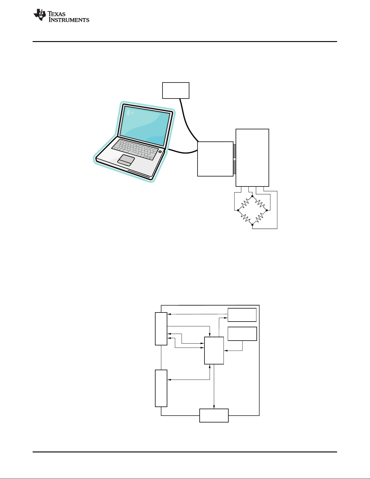
Figure 9 shows the block diagram for the USB-DAQ-Platform. This platform is a general-purpose data
acquisition system that is used on several different Texas Instruments evaluation modules. The details of
its operation are included in a separate document (available for download at www.ti.com). The block
diagram shown in Figure 9 gives a brief overview of the platform. The primary control device on the
USB-DAQ-Platform is the TUSB3210.
www.ti.com
3 PGA309EVM-USB Hardware Setup
3.1 Electrostatic Discharge Warning
16
Figure 9. Theory of Operation For USB-DAQ-Platform
The PGA309EVM-USB Hardware setup involves connecting the two halves of the EVM together, applying
power, connecting the USB cable, and setting the jumpers. This section covers the details of this
procedure.
Many of the components on the PBA309EVM-USB are susceptible to damage by electrostatic discharge
(ESD). Customers are advised to observe proper ESD handling precautions when unpacking and handling
the EVM, including the use of a grounded wrist strap at an approved ESD workstation.
CAUTION
Failure to observe ESD handling procedures may result in damage to EVM
components.
PGA309EVM-USB SBOU084–February 2010
Copyright © 2010, Texas Instruments Incorporated
Submit Documentation Feedback
Page 17

www.ti.com
3.2 Typical Hardware Connections
To set up the PGA309EVM-USB hardware, connect the two halves of the EVM together, apply power, and
then connect the external sensor. Figure 10 shows the typical hardware connections.
PGA309EVM-USB Hardware Setup
Figure 10. PGA309EVM-USB Typical Hardware Connections
SBOU084–February 2010 PGA309EVM-USB
Submit Documentation Feedback
Copyright © 2010, Texas Instruments Incorporated
17
Page 18

PGA309EVM-USB Hardware Setup
3.3 Connecting the Hardware
To connect the two PCBs of the PGA309EVM-USB together, gently push on both sides of the D-SUB
connectors (as shown in Figure 11). Make sure that the two connectors are completely pushed together;
that is, loose connections may cause intermittent operation.
www.ti.com
18
Figure 11. Connecting the Two EVM PCBs
PGA309EVM-USB SBOU084–February 2010
Submit Documentation Feedback
Copyright © 2010, Texas Instruments Incorporated
Page 19

www.ti.com
3.4 Connecting Power
After the two parts of the PGA309EVM-USB are connected, as shown in Figure 12, connect the power to
the EVM. Always connect power before connecting the USB cable. If you connect the USB cable before
connecting the power, the computer will attempt to communicate with an unpowered device that will not be
able to respond.
PGA309EVM-USB Hardware Setup
Figure 12. Connecting Power to the EVM
SBOU084–February 2010 PGA309EVM-USB
Submit Documentation Feedback
Copyright © 2010, Texas Instruments Incorporated
19
Page 20

PGA309EVM-USB Hardware Setup
3.5 Connecting the USB Cable to the PGA309EVM-USB
Figure 13 shows the typical response to connecting the USB-DAQ-Platform to a PC USB port for the first
time. Note that the EVM must be powered on before connecting the USB cable. Typically, the computer
will respond with a Found New Hardware, USB Device pop-up. The pop-up typically changes to Found
New Hardware, USB Human Interface Device. This pop-up indicates that the device is ready to be used.
The USB DAQ platform uses the Human Interface Device Drivers that are part of the Microsoft®Windows
operating system.
In some cases, the Windows Add Hardware Wizard will pop up. If this prompt occurs, allow the system
device manager to install the Human Interface Drivers by clicking Yes when requested to install drivers.
www.ti.com
®
20
Figure 13. Connecting the USB Cable
PGA309EVM-USB SBOU084–February 2010
Submit Documentation Feedback
Copyright © 2010, Texas Instruments Incorporated
Page 21

www.ti.com
3.6 PGA309EVM-USB Jumper Settings
Figure 14 illustrates the default jumpers configuration for the PGA309_Test_Board. In general, the jumper
settings of the USB-DAQ-Platform do not need to be changed. You may want to change some of the
jumpers on the PGA309_Test_Board to match your specific sensor conditioning design.
PGA309EVM-USB Hardware Setup
Figure 14. Default Jumper Settings (PGA309_Test_Board)
SBOU084–February 2010 PGA309EVM-USB
Submit Documentation Feedback
Copyright © 2010, Texas Instruments Incorporated
21
Page 22

PGA309EVM-USB Hardware Setup
Figure 15 shows the default jumpers configuration for the USB-DAQ-Platform. In general, the jumper
settings of the USB-DAQ-Platform do not need to be changed.
www.ti.com
22
Figure 15. Default Jumper Settings (USB-DAQ-Platform)
Table 4 explains the function of the jumpers on the PGA309_Test_Board.
Table 4. PGA309_Test_Board Jumper Functions: General
Jumper Default Purpose
JMP10 NC This jumper is used to connect the current loop output
JMP11 V
JMP9 NC This jumper connects the V
PGA309EVM-USB SBOU084–February 2010
Copyright © 2010, Texas Instruments Incorporated
power This jumper is used to connect the current-loop output
DUT
(XTR117). For voltage output modules, set this jumper to the NC
(no connect) position. For current-loop modules, set this jumper
to the Vref PGA position.
(XTR117). For voltage output modules, set this jumper to the
Vdut Power (5V connected to power) position. For current-loop
modules, set this jumper to the Loop Power (power to loop
supply) position.
pin on the PGA309 to the
XTR117 input. For voltage output modules, set this jumper to the
NC (no connect) position. For current-loop modules, set this
jumper to the Vout to XTR position.
OUT
Submit Documentation Feedback
Page 23

www.ti.com
Table 5 describes the function of the jumpers in the Miscellaneous connections section of the PGA309
Test Board.
PGA309EVM-USB Hardware Setup
Table 5. PGA309_Test_Board Jumper Functions: Miscellaneous Connections
Jumper Default Purpose
JMP1, JMP2 NC For JMP1 = NC, JMP2 = V
PGA309 is configured for internal reference. In this mode, JMP2
is not connected, so its position does not matter.
V
EXT For JMP1 = V
REF
external reference and is connected to VS.
For JMP1 = V
configured for external reference and is connected to T2
, JMP2 = VS: The REF pin is configured for
REF
, and JMP2 = V
REF
(terminal for external reference connection).
JMP3 ADS1 For JMP3 = ADS1, it connects the analog-to-digital converter
(ADC) on the USB-DAQ-Platform to the output of the PGA309.
The ADC on the USB-DAQ-Platform allows full measurement
and calibration of the PGA309 without any additional
instruments.
For JMP3 = NC, the ADC on the USB-DAQ-Platform is not
connected to the PGA309. This mode is useful if you want to
use an external DMM in place of the USB-DAQ ADC.
JMP7, JMP8 NC For JMP7 = NC, and JMP8 = One to PRG: In this mode, the
one-wire signal from the USB-DAQ-Platform is connected
directly to the PRG pin on the PGA309. This mode is commonly
called Four-wire mode because only four connections are
required (Power, GND, V
One to PRG For JMP7 = V
mode, the one-wire signal from the USB-DAQ-Platform is
connected to the V
commonly called Three-wire mode because only three
to PRG, and JMP8 = One to V
OUT
/PRG pin on the PGA309. This mode is
OUT
connections are required (Power, GND, and V
EXT: The REF pin on the
REF
EXT: The REF pin is
REF
, and PRG).
OUT
OUT
: In this
OUT
/PRG).
Table 6 explains the function of the jumpers in the sensor emulator section connections section of the
PGA309 Test Board.
Table 6. PGA309_Test_Board Jumper Functions: Sensor Emulator Section
Jumper Default Purpose
JMP12 V
EXC
JMP17, JMP4, JMP5, JMP6 Emulate These jumpers select the sensor emulator when in the Emulate
JMP14, JMP15 10mV These jumpers select the range of the sensor emulator.
JMP13, JMP16 RT–, Diode This jumper selects the type of temperature sensor you will
This jumper selects VSor V
emulator. Using VSas the reference is commonly called
as the reference for the sensor
EXC
ratiometric mode.
position. When the jumper is in the EXT position, it selects the
external sensor.
This jumper is used for the sensor emulator only; its position is
not important for externally-connected, real-world sensors.
10m = maximum emulator output is 10mV/V.
100m = maximum emulator output is 100mV/V.
emulate on the EVM. This jumper is used for the sensor
emulator only; its position is not important for
externally-connected, real-world sensors.
JMP13 = Diode, JMP16 = RT-. In this position, the temperature
sensor emulation is set for diode type temperature sensor.
When JMP13 = Diode, the position of JMP16 does not matter.
JMP13 = RT, JMP16 = RT-. In this position, the temperature
sensor emulation is set for RT–.
JMP13 = RT, JMP16 = RT+. In this position, the temperature
sensor emulation is set for RT+.
SBOU084–February 2010 PGA309EVM-USB
Submit Documentation Feedback
Copyright © 2010, Texas Instruments Incorporated
23
Page 24

PGA309EVM-USB Hardware Setup
Table 7 explains the function of the USB-DAQ-Platform jumpers. For most applications the default jumper
position should be used. A separate document gives details regarding the operation and design of the
USB-DAQ-Platform.
Jumper Default Purpose
JUMP1 EXT This jumper selects external power or bus power. External
JUMP2 EXT Same as JUMP1.
JUMP3 EE ON This jumper determines where the PGA309 gets its power
JUMP4, JUMP5 L, L This jumper sets the address for the USB board. The only
JUMP9 5V This jumper selects the voltage of the device under test supply
JUMP10 WP ON This jumper write-protects the firmware EEPROM.
JUMP11 WP ON This jumper write-protects the calibration EEPROM
JUMP13 Reg This jumper configures the regulator output to generate the V
JUMP14 9V This jumper configures the external power (9V as apposed to
JUMP17 BUS While in the BUS position V
JUMP18 V
Table 7. USB-DAQ-Platform Jumper Settings
power is applied on J5 or T3 (9V dc). Bus power is 5V from the
USB bus. External power is typically used because the USB bus
power is noisy.
DUT
supply. In the V
default is the V
connected externally.
reason to change from the default is if multiple boards are being
used.
(V
= 5V or 3V)
DUT
supply. The USB bus can be used as the V
the bus)
V
position, the V
RAW
source. This allows for any value of V
Connects the pull-up resistor on GPIO to the V
VCCsupply.
position, the EVM provides power. The
DUT
position. In the V
DUT
supply is connected to an external
DUT
www.ti.com
position, the power is
S_Ext
supply.
DUT
operation is normal. While in the
DUT
between 3V and 5V.
DUT
supply or the
DUT
DUT
Adjusting the value of V
CAUTION
beyond the range of 3V to 5V will damage the EVM.
DUT
24
PGA309EVM-USB SBOU084–February 2010
Submit Documentation Feedback
Copyright © 2010, Texas Instruments Incorporated
Page 25

www.ti.com
4 PGA309EVM-USB Software Overview
This section discusses how to install and use the PGA309EVM-USB software.
4.1 Operating Systems for PGA309 Software
The PGA309EVM-USB software has been tested on the Microsoft Windows XP operating system (OS)
with United States and European regional settings. The software should also function on other Windows
operating systems. Please report any OS compatibility issues to precisionamps@list.ti.com.
4.2 PGA309EVM-USB Software Install
Follow these steps to install the PGA309EVM-USB software:
Step 1. Software can be downloaded from the PGA309EVM-USB web page, or from the disk
included with the PGA309EVM-USB, which contains a folder called Install_software/.
Step 2. Find the file called setup.exe. Double-click the file to start the installation process.
Step 3. Follow the on-screen prompts to install the software.
Step 4. To remove the application, use the Windows Control Panel utility, Add/Remove Software.
4.3 Starting the PGA309EVM-USB Software
The PGA309EVM-USB software can be operated through the Windows Start menu. From Start, select All
Programs; then select the PGA309EVM-USB program. Refer to Figure 16 for a screenshot of how the
software should appear if the EVM is functioning properly.
PGA309EVM-USB Software Overview
4.4 Using the PGA309EVM-USB Software
The PGA309EVM-USB software has five different primary tabs that allow users to access different
features of the PGA309 itself. Each tab is designed to provide an intuitive graphical interface that will help
users to gain a better understanding of the device.
SBOU084–February 2010 PGA309EVM-USB
Submit Documentation Feedback
Copyright © 2010, Texas Instruments Incorporated
25
Page 26

PGA309EVM-USB Software Overview
4.5 Registers Tab
Figure 16 illustrates the Registers tab.
www.ti.com
Figure 16. PGA309EVM-USB Software: Registers Tab
This tab presents a Register Table that shows a summary of the PGA309 device registers. You can select
and toggle various sections of the table by clicking on the table with your mouse. For example, when a
row is selected, it will be highlighted in blue in the table. The 16 individual bits in the selected register are
displayed below the register table. Note that each bit has descriptive text above the bit that identifies or
defines the function of that bit. You can edit the bit value by using the up (↑) or down (↓) arrow to the left
of the bit. Any changes made to the bit are displayed in the table. Additionally, changes to the device
registers initiated on other tabs in the software will also update the Registers tab.
26
PGA309EVM-USB SBOU084–February 2010
Submit Documentation Feedback
Copyright © 2010, Texas Instruments Incorporated
Page 27

www.ti.com
4.6 EEPROM Table Tab
The EEPROM Table tab is shown in Figure 17.
PGA309EVM-USB Software Overview
Figure 17. PGA309EVM-USB Software: EEPROM Tab
This tab offers a debug utility that allows you to view, load, edit, and save various EEPROM values. This
tab also contains displays for the two different sections of the PGA309 EEPROM. However, most users
will create the EEPROM table itself using the features of the Auto-Calibrate tab.
SBOU084–February 2010 PGA309EVM-USB
Submit Documentation Feedback
Copyright © 2010, Texas Instruments Incorporated
27
Page 28

PGA309EVM-USB Software Overview
4.7 Block Diagram Tab
The Block Diagram tab (shown in Figure 18) gives you full access to all the elements in the PGA309.
Making a change to the block diagram is reflected in the Register Table (see Section 4.5). This feature is
helpful when experimenting with your specific setup.
www.ti.com
28
Figure 18. PGA309EVM-USB Software: Block Diagram
PGA309EVM-USB SBOU084–February 2010
Submit Documentation Feedback
Copyright © 2010, Texas Instruments Incorporated
Page 29

www.ti.com
4.8 Auto Calibrate Tab
The Auto Calibrate tab is used to calibrate a PGA309 module over temperature. This process can be done
with a real-world sensor or with an emulated sensor. It is recommended that you first become familiar with
the calibration process by using the sensor emulator. Once the user completely understands the
calibration process, the user can connect a real-world sensor to the EVM.
Additionally, this tab contains several sub-tabs that are used to configure the PGA309 device for particular
test applications. This section explains each sub-tab in detail.
4.8.1 Sensor Definition Functions
Figure 19 shows the Sensor Definition sub-tab.
PGA309EVM-USB Software Overview
Figure 19. PGA309EVM-USB Software: Auto Calibrate Tab—Sensor Definition
Use the Sensor Definition sub-tab to configure the sensor emulator before starting the calibration process.
If you are not using the sensor emulator, you can skip this tab. If you are using the sensor emulator, enter
your sensor information in one of two different formats using the Select Data Mode option box.
• Sensor Data Mode: Sensor Characteristics
Enter the sensor characteristics as they are typically given in product data sheets (that is, span, offset,
drift, and nonlinearity values).
• Sensor Data Mode: Raw Sensor Data
Enter sensor data that has been measured at three temperatures (room or ambient, hot, and cold).
SBOU084–February 2010 PGA309EVM-USB
Submit Documentation Feedback
Copyright © 2010, Texas Instruments Incorporated
29
Page 30

PGA309EVM-USB Software Overview
Select the type of temperature sensor that you want to emulate using the Define Temperature Sensor
Model control. Depending on the type of temperature sensor selected, you may need to provide some
additional information about the sensor (for example, RTresistance, Bridge Resistance, and drift). You
may also need to set the sensor emulator range. The sensor emulator has two jumper-selected ranges
(10mV/V and 100mV/V). The software must be set to match the jumper setting. Observe the sensor
emulator graphs using the Open Sensor Emulator Control Panel button.
Figure 20 shows the sensor emulator control tool.
www.ti.com
30
Figure 20. PGA309EVM-USB Software: Sensor Emulator Control Panel Tool
The Sensor Emulator Control Tool is a pop-up window that can be accessed from the Sensor Definition
sub-tab. It displays three graphs that show the operation of the emulated sensor under different pressures
and at different temperatures. The two sliders below the graphs adjust the operating point of the sensor
emulator. When you adjust the sliders, the cursors on the graph move accordingly to the new operating
point. The sensor output (in mV/V) is displayed to the right of the sliders. You can test your calibration at
any temperature and pressure using this tool.
PGA309EVM-USB SBOU084–February 2010
Submit Documentation Feedback
Copyright © 2010, Texas Instruments Incorporated
Page 31

www.ti.com
4.8.2 PGA Setup Functions
Figure 21 illustrates the PGA Setup sub-tab.
PGA309EVM-USB Software Overview
Figure 21. PGA309EVM-USB Software: Auto Calibrate Tab—PGA Setup
The PGA Setup sub-tab is divided into six sections. Each section is identified as a sequential step:
Step 1. PGA309 Hardware Connections
Step 2. PGA309 Initial Register Settings
Step 3. Sensor Model (temperature sensor connection, temperature range)
Step 4. Calibration Range (output voltage or current range)
Step 5. Calibration Measure Points (temperature and nonlinearity)
Step 6. Step 6 confirms the previous entries and configures the DUT settings.
The last procedure in the setup process is to save the settings from this tab. If you have already made a
sensor setup file, you can skip Steps 1 to 6 and simply load the file; select the Load Sensor Setup button
at the lower right-hand side of the window.
SBOU084–February 2010 PGA309EVM-USB
Submit Documentation Feedback
Copyright © 2010, Texas Instruments Incorporated
31
Page 32

PGA309EVM-USB Software Overview
4.8.3 Two-Point Calibration and Linearization Functions
The Two-Point Calibration and Linearization sub-tab is illustrated in Figure 22.
www.ti.com
Figure 22. PGA309EVM-USB Software: Auto Calibrate Tab—Two-Point Calibration and Linearization
This sub-tab performs the room temperature calibration. To perform this calibration with the sensor
emulator, press the buttons labeled Step 1 through Step 6, respectively. The sensor emulator
automatically adjusts the simulated load according to what is required for each step. To perform the
calibration using a real-world sensor, you must adjust the load applied to the sensor before pressing each
button. For example, adjust the load (that is, decrease the pressure) to the minimum level before pressing
the Step 1 button. The software will take readings and adjust the gain and offset in order to obtain the
desired output swing.
32
PGA309EVM-USB SBOU084–February 2010
Submit Documentation Feedback
Copyright © 2010, Texas Instruments Incorporated
Page 33

www.ti.com
4.8.4 Temperature Error Compensation Functions
Figure 23 shows the Temperature Error Compensation sub-tab.
PGA309EVM-USB Software Overview
Figure 23. PGA309EVM-USB Software: Auto Calibrate Tab—Temperature Error Compensation
The Temperature Error Compensation sub-tab is divided into six separate measurements (refer to
Figure 23). When using the sensor emulator option, you can complete the calibration by pressing the
Read button six times. Each time the Read button is pressed, the sensor emulator adjusts the
temperature signal and the bridge signal automatically to correspond to the temperature and load
required. For real-world sensors, however, the EVM must be physically placed in an environmental
chamber; the user must then adjust the temperature and applied load as required by the table. When all
six measurements are completed, press the Calculate and download LUT button to update the
EEPROM look-up table (LUT). After pressing the Calculate and download LUT button, the module is
calibrated, and should output the desired voltage according to the specified load and temperature.
SBOU084–February 2010 PGA309EVM-USB
Submit Documentation Feedback
Copyright © 2010, Texas Instruments Incorporated
33
Page 34

PGA309EVM-USB Software Overview
4.8.5 Post Cal Error Check
The Post Cal Error Check sub-tab is illustrated in Figure 24.
www.ti.com
Figure 24. PGA309EVM-USB Software: Auto Calibrate Tab—Post Cal Error Check
This sub-tab is used to test post-calibration accuracy. This feature only works for the sensor emulator
mode. Press the Read Post Calibration Results button, and the software automatically adjusts the
sensor emulator to read the output over the calibration range. (Typical error is less than 0.1%.)
34
PGA309EVM-USB SBOU084–February 2010
Submit Documentation Feedback
Copyright © 2010, Texas Instruments Incorporated
Page 35

www.ti.com
4.8.6 DMM Options
Figure 25 shows the DMM Options sub-tab.
PGA309EVM-USB Software Overview
Figure 25. PGA309EVM-USB Software: Auto Calibrate Tab—DMM Options
It is possible to use an external digital multimeter (or DMM) to calibrate sensor modules. The current
version of the PGA309EBM-USB software provides the capability for the Agilent 34401A DMM combined
with a National Instruments GPIB-USB- HS. To change the external DMM settings, select the Measuring
Mode button and choose the desired measurement tool. Then select the DVM Connection (VISA name)
to choose the IEEE488 address.
SBOU084–February 2010 PGA309EVM-USB
Submit Documentation Feedback
Copyright © 2010, Texas Instruments Incorporated
35
Page 36

Evaluation Board/Kit Important Notice
Texas Instruments (TI) provides the enclosed product(s) under the following conditions:
This evaluation board/kit is intended for use for ENGINEERING DEVELOPMENT, DEMONSTRATION, OR EVALUATION
PURPOSES ONLY and is not considered by TI to be a finished end-product fit for general consumer use. Persons handling the
product(s) must have electronics training and observe good engineering practice standards. As such, the goods being provided are
not intended to be complete in terms of required design-, marketing-, and/or manufacturing-related protective considerations,
including product safety and environmental measures typically found in end products that incorporate such semiconductor
components or circuit boards. This evaluation board/kit does not fall within the scope of the European Union directives regarding
electromagnetic compatibility, restricted substances (RoHS), recycling (WEEE), FCC, CE or UL, and therefore may not meet the
technical requirements of these directives or other related directives.
Should this evaluation board/kit not meet the specifications indicated in the User’s Guide, the board/kit may be returned within 30
days from the date of delivery for a full refund. THE FOREGOING WARRANTY IS THE EXCLUSIVE WARRANTY MADE BY
SELLER TO BUYER AND IS IN LIEU OF ALL OTHER WARRANTIES, EXPRESSED, IMPLIED, OR STATUTORY, INCLUDING
ANY WARRANTY OF MERCHANTABILITY OR FITNESS FOR ANY PARTICULAR PURPOSE.
The user assumes all responsibility and liability for proper and safe handling of the goods. Further, the user indemnifies TI from all
claims arising from the handling or use of the goods. Due to the open construction of the product, it is the user’s responsibility to
take any and all appropriate precautions with regard to electrostatic discharge.
EXCEPT TO THE EXTENT OF THE INDEMNITY SET FORTH ABOVE, NEITHER PARTY SHALL BE LIABLE TO THE OTHER
FOR ANY INDIRECT, SPECIAL, INCIDENTAL, OR CONSEQUENTIAL DAMAGES.
TI currently deals with a variety of customers for products, and therefore our arrangement with the user is not exclusive.
TI assumes no liability for applications assistance, customer product design, software performance, or infringement of
patents or services described herein.
Please read the User’s Guide and, specifically, the Warnings and Restrictions notice in the User’s Guide prior to handling the
product. This notice contains important safety information about temperatures and voltages. For additional information on TI’s
environmental and/or safety programs, please contact the TI application engineer or visit www.ti.com/esh.
No license is granted under any patent right or other intellectual property right of TI covering or relating to any machine, process, or
combination in which such TI products or services might be or are used.
FCC Warning
This evaluation board/kit is intended for use for ENGINEERING DEVELOPMENT, DEMONSTRATION, OR EVALUATION
PURPOSES ONLY and is not considered by TI to be a finished end-product fit for general consumer use. It generates, uses, and
can radiate radio frequency energy and has not been tested for compliance with the limits of computing devices pursuant to part 15
of FCC rules, which are designed to provide reasonable protection against radio frequency interference. Operation of this
equipment in other environments may cause interference with radio communications, in which case the user at his own expense
will be required to take whatever measures may be required to correct this interference.
EVM Warnings and Restrictions
It is important to operate this EVM within the input voltage range of 5.7V to 9V and the output voltage range of 0V to 5V.
Exceeding the specified input range may cause unexpected operation and/or irreversible damage to the EVM. If there are
questions concerning the input range, please contact a TI field representative prior to connecting the input power.
Applying loads outside of the specified output range may result in unintended operation and/or possible permanent damage to the
EVM. Please consult the EVM User's Guide prior to connecting any load to the EVM output. If there is uncertainty as to the load
specification, please contact a TI field representative.
During normal operation, some circuit components may have case temperatures greater than +50°C. The EVM is designed to
operate properly with certain components above +125°C as long as the input and output ranges are maintained. These
components include but are not limited to linear regulators, switching transistors, pass transistors, and current sense resistors.
These types of devices can be identified using the EVM schematic located in the EVM User's Guide. When placing measurement
probes near these devices during operation, please be aware that these devices may be very warm to the touch.
Mailing Address: Texas Instruments, Post Office Box 655303, Dallas, Texas 75265
Copyright © 2010, Texas Instruments Incorporated
Page 37

IMPORTANT NOTICE
Texas Instruments Incorporated and its subsidiaries (TI) reserve the right to make corrections, modifications, enhancements, improvements,
and other changes to its products and services at any time and to discontinue any product or service without notice. Customers should
obtain the latest relevant information before placing orders and should verify that such information is current and complete. All products are
sold subject to TI’s terms and conditions of sale supplied at the time of order acknowledgment.
TI warrants performance of its hardware products to the specifications applicable at the time of sale in accordance with TI’s standard
warranty. Testing and other quality control techniques are used to the extent TI deems necessary to support this warranty. Except where
mandated by government requirements, testing of all parameters of each product is not necessarily performed.
TI assumes no liability for applications assistance or customer product design. Customers are responsible for their products and
applications using TI components. To minimize the risks associated with customer products and applications, customers should provide
adequate design and operating safeguards.
TI does not warrant or represent that any license, either express or implied, is granted under any TI patent right, copyright, mask work right,
or other TI intellectual property right relating to any combination, machine, or process in which TI products or services are used. Information
published by TI regarding third-party products or services does not constitute a license from TI to use such products or services or a
warranty or endorsement thereof. Use of such information may require a license from a third party under the patents or other intellectual
property of the third party, or a license from TI under the patents or other intellectual property of TI.
Reproduction of TI information in TI data books or data sheets is permissible only if reproduction is without alteration and is accompanied
by all associated warranties, conditions, limitations, and notices. Reproduction of this information with alteration is an unfair and deceptive
business practice. TI is not responsible or liable for such altered documentation. Information of third parties may be subject to additional
restrictions.
Resale of TI products or services with statements different from or beyond the parameters stated by TI for that product or service voids all
express and any implied warranties for the associated TI product or service and is an unfair and deceptive business practice. TI is not
responsible or liable for any such statements.
TI products are not authorized for use in safety-critical applications (such as life support) where a failure of the TI product would reasonably
be expected to cause severe personal injury or death, unless officers of the parties have executed an agreement specifically governing
such use. Buyers represent that they have all necessary expertise in the safety and regulatory ramifications of their applications, and
acknowledge and agree that they are solely responsible for all legal, regulatory and safety-related requirements concerning their products
and any use of TI products in such safety-critical applications, notwithstanding any applications-related information or support that may be
provided by TI. Further, Buyers must fully indemnify TI and its representatives against any damages arising out of the use of TI products in
such safety-critical applications.
TI products are neither designed nor intended for use in military/aerospace applications or environments unless the TI products are
specifically designated by TI as military-grade or "enhanced plastic." Only products designated by TI as military-grade meet military
specifications. Buyers acknowledge and agree that any such use of TI products which TI has not designated as military-grade is solely at
the Buyer's risk, and that they are solely responsible for compliance with all legal and regulatory requirements in connection with such use.
TI products are neither designed nor intended for use in automotive applications or environments unless the specific TI products are
designated by TI as compliant with ISO/TS 16949 requirements. Buyers acknowledge and agree that, if they use any non-designated
products in automotive applications, TI will not be responsible for any failure to meet such requirements.
Following are URLs where you can obtain information on other Texas Instruments products and application solutions:
Products Applications
Amplifiers amplifier.ti.com Audio www.ti.com/audio
Data Converters dataconverter.ti.com Automotive www.ti.com/automotive
DLP® Products www.dlp.com Communications and www.ti.com/communications
DSP dsp.ti.com Computers and www.ti.com/computers
Clocks and Timers www.ti.com/clocks Consumer Electronics www.ti.com/consumer-apps
Interface interface.ti.com Energy www.ti.com/energy
Logic logic.ti.com Industrial www.ti.com/industrial
Power Mgmt power.ti.com Medical www.ti.com/medical
Microcontrollers microcontroller.ti.com Security www.ti.com/security
RFID www.ti-rfid.com Space, Avionics & www.ti.com/space-avionics-defense
RF/IF and ZigBee® Solutions www.ti.com/lprf Video and Imaging www.ti.com/video
Mailing Address: Texas Instruments, Post Office Box 655303, Dallas, Texas 75265
Copyright © 2010, Texas Instruments Incorporated
Telecom
Peripherals
Defense
Wireless www.ti.com/wireless-apps
 Loading...