

Please be aware that an important notice concerning availability, standard warranty, and use in critical applications of Texas Instruments
)
查询PGA309供应商
PROGRAMMABLE SENSOR CONDITIONER
PGA309
SBOS292A − DECEMBER 2003 − REVISED AUGUST 2004
Voltage Output
FEATURES
D COMPLETE BRIDGE SENSOR CONDITIONER
D VOLTAGE OUTPUT: Ratiometric or Absolute
D DIGITAL CAL: No Po tent io meters/ Sen so r Trims
D SENSOR ERROR COMPENSATION
− Span, Offset, and Temperature Drifts
D LOW ERROR, TIME-STABLE
D SENSOR LINEARIZATION CIRCUITRY
D TEMPERATURE SENSE: Internal or External
D CALIBRATION LOOKUP TABLE LOGIC
− Uses External EEPROM (SOT23-5)
D OVER/UNDER-SCALE LIMITING
D SENSOR FAULT DETECTION
D +2.7V TO +5.5V OPERATION
D −40°C to +125°C OPERATION
D SMALL TSSOP-16 PACKAGE
APPLICATIONS
D BRIDGE SENSORS
D REMOTE 4-20mA TRANSMITTERS
D STRAIN, LOAD, AND WEIGH SCALES
D AUTOMOTIVE SENSORS
EVALUATION TOOLS
D HARDWARE DESIGNER’S KIT (PGA309EVM)
− Temperature Eval of PGA309 + Sensor
− Full Programming of PGA309
− Sensor Compensation Analysis Tool
P
psi
0
50
No nlinear
Bridge
Transducer
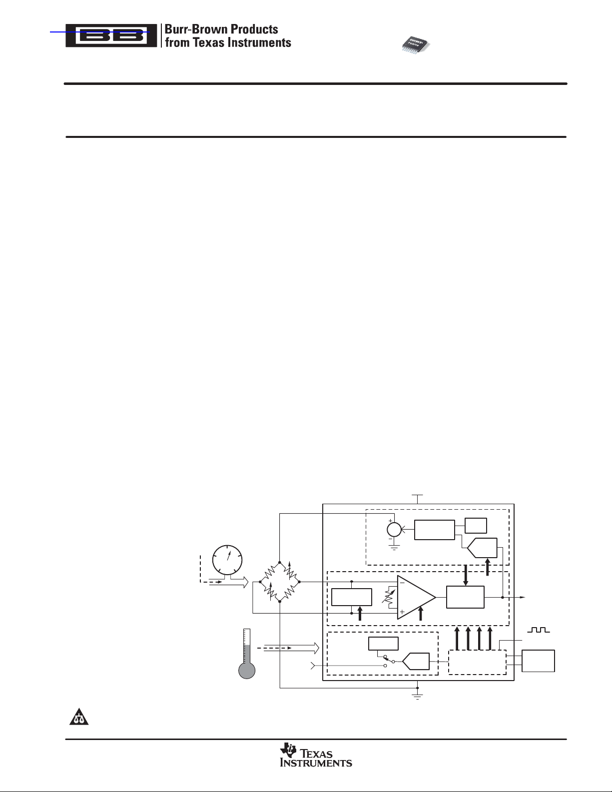
DESCRIPTION
The PGA309 is a programmable a nalog s ignal c onditioner
designed for bridge sensors. The analog signal path amplifies the sensor signal and provides digital calibration for
zero, span, zero drift, span drift, and sensor linearization
errors with a ppl ie d s tress ( pre ssure , strain, e tc.). The calibration is done via a One-Wire digital serial interfac e or
through a Two-Wire industry-standard connection. The
calibration paramet ers are stored in external nonvolatile
memory (typically SOT23-5) to eliminate manual trimming
and achieve long-term st ability.
The all-analog signal path contains a 2x2 input m ultiplexer (mux), auto-zero programmable-gain instrum entation
amplifier, linearization circuit, voltage refer ence, internal
oscillator, control logic, and an output amplifier. Programmable level shifting compens ates for sensor DC offsets.
The core of the PGA309 is the precision, low-drift, no 1/f
noise Front-End PGA (Programmable Gain Amplifier).
The overall gain of the Front-End PGA + Output Amplifier
can be adjusted from 2.7V/V to 1152V/V. The polarity of
the inputs can be switched through the input mux to accommodate sens ors with unknown polarity output. The
Fault Monit or cir cuit detects and signals sens or burnout,
overload, and syst em fault condit ions .
For deta iled applic at ion infor ma tion, s ee t he PGA309
User’s Gui de (SBO U024), avai lable for dow nload at
www.ti.c om .
V
PGA309
EXC
Analog Sensor Linearization
V
S
Linearization
Circuit
Ref
Lin DAC
Fault
Monitor
+125_ C
Digital
T
−40_C
semiconductor products and disclaimers thereto appears at the end of this data sheet.
All trademarks are the property of their respective owners.
! !
Ext Temp
www.ti.com
Temperature
Compensation
ExtTemp
Auto−Zero
PGA
IntTemp
Temp
ADC
Copyright 2003−2004, Texas Instruments Incorporated
Over/Under
Scale Limiter
AnalogSignalConditioning
Control Register
Interface Circuitry
Linear
V
OUT
DigitalCal
EEPROM
(SOT23−5
"#$%
SBOS292A − DECEMBER 2003 − REVISED AUGUST 2004
www.ti.com
(1)
−0.3V to VSA +0.3V. . . . . . . . . . . . . . . . . . . . .
(1)
TEMPERATURE
+7.0V. . . . . . . . . . . . . . . . . . . . . . . . . . . . . . . . . .
±150mA. . . . . . . . . . . . . . . . . . . . . . . . . . . . . . . . .
SPECIFIED
RANGE
proper handling and installation procedures can cause damage.
ESD damage can range from subtle performance degradation to
complete device failure. Precision integrated circuits may be more
susceptible t o damage because very small parametric changes could
cause the device not to meet its published specifications.
PACKAGE/ORDERING INFORMATION
PACKAGE
PRODUCT PACKAGE−LEAD
PGA309 TSSOP-16 PW −40°C to +125°C PGA309
(1)
For the most current package and ordering information, refer to our web site at www.ti.com.
DRAWING
ABSOLUTE MAXIMUM RATINGS
Over operating free-air temperature range unless otherwise noted.
Supply Voltage, VSD, V
Input Voltage, V
Input Current, VFB, V
Input Current ±10mA. . . . . . . . . . . . . . . . . . . . . . . . . . . . . . . . . . . . . . . . . . . .
Output Current Limit 50mA. . . . . . . . . . . . . . . . . . . . . . . . . . . . . . . . . . . . . . . . .
Storage Temperature Range −60°C to +150°C. . . . . . . . . . . . . . . . . . . . . . . .
Operating Temperature Range −55°C to +150°C. . . . . . . . . . . . . . . . . . . . . .
Junction Temperature +150°C. . . . . . . . . . . . . . . . . . . . . . . . . . . . . . . . . . . . .
Lead Temperature (soldering, 10s) +300°C. . . . . . . . . . . . . . . . . . . . . . . . . . .
ESD Protection (Human Body Model) 4kV. . . . . . . . . . . . . . . . . . . . . . . . . . .
(1)
Stresses above these ratings may cause permanent damage.
IN1
, V
SD
IN2
OUT
(2)
Exposure to absolute maximum conditions for extended periods
may degrade device reliability. These are stress ratings only , an d
functional operation of the device at these or any other conditions
beyond those specified is not implied.
(2)
Input terminals are diode-clamped to the power-supply rails.
Input signals that can swing more than 0.5V beyond the supply
rails should be current limited to 10mA or less.
PACKAGE
MARKING
ORDERING
NUMBER
PGA309AIPWR Tape and Reel, 2500
PGA309AIPWT Tape and Reel, 250
TRANSPORT MEDIA,
QUANTITY
This integrated circuit can be damaged by ESD. Texas
Instruments recommends that all integrated circuits be
handled with appropriate precautions. Failure to observe
2
"#$%
www.ti.com
SBOS292A − DECEMBER 2003 − REVISED AUGUST 2004
ELECTRICAL CHARACTERISTICS
BOLDFACE limits apply over the specified temperature range: TA = −40°C to +125°C
TA = +25°C, VSA = VSD = +5V (VSA = V
unless otherwise noted.
PARAMETER CONDITIONS MIN TYP MAX UNITS
FRONT-END PGA + OUTPUT AMPLIFIER
V
V
V
V
V
External Sensor Output Sensitivity VSA = VSD = V
FRONT-END PGA
Auto-Zero Internal Frequency 7 kHz
Offset Voltage (RTI)
Linear Input Voltage Range
Input Bias Current 0.1 1.5 nA
Input Impedance: Differential 30 || 6 GΩ || pF
Input Impedance: Common-Mode 50 || 20 GΩ || pF
Input Voltage Noise 0.1Hz to 10Hz, GF = 128 4 µV
PGA Gain
Output Voltage Range 0.05 to VSA − 0.1 V
Bandwidth Gain = 4 400 kHz
COARSE OFFSET ADJUST
(RTI OF FRONT-END PGA)
Range ±(14)(V
Resolution ±14 steps, 4-Bit + Sign 4 mV
FINE OFFSET ADJUST (ZERO DAC)
(RTO of the Front-End PGA)
Programming Range 0 V
Output Range 0.1 VSA−0.1 V
Resolution 65,536 steps, 16-Bit DAC 73 µV
Integral Nonlinearity 20 LSB
Differential Nonlinearity 0.5 LSB
Gain Error 0.1 %
Gain Error Drift 10 ppm/°C
Offset 5 mV
Offset Drift 10 µV/°C
OUTPUT FINE GAIN ADJUST (GAIN DAC)
Range 0.33 to 1 V/V
Resolution 65,536 steps, 16-Bit DAC 10 µV/V
Integral NonLinearity 20 LSB
Differential NonLinearity 0.5 LSB
Differential Signal Gain Range
OUT/VIN
Slew Rate 0.5 V/µs
OUT
Settling Time (0.01%) V
OUT
Settling Time (0.01%) V
OUT
Nonlinearity 0.002 %FSR
OUT
(2)
vs Temperature +0.2 µV/°C
vs Supply Voltage, V
vs Common-Mode Voltage GF = Front-End PGA Gain 1500/GF6000/G
Gain Range Steps 4, 8, 16, 23.27, 32, 42.67, 64, 128 4 to 128 V/V
Initial Gain Error GF = 4 to 42 0.2 ±1 %
vs Temperature 10 ppm/°C
vs Temperature 0.004 %/°C
SA
SUPPLY ANALOG
(1)
(3)
(2)
, VSD = V
SUPPLY DIGITAL
Front-End PGA Gains: 4, 8, 16, 23.27, 32, 42.67, 64, 128
Output Amplifier Gains: 2, 2.4, 3, 3.6, 4.5, 6, 9
OUT/VIN
OUT/VIN
Fine Gain Adjust = 1
Differential Gain = 8, RL = 5kΩ || 200pF 6 µs
Differential Gain = 191, RL = 5kΩ || 200pF 4.1 µs
Coarse Offset Adjust Disabled ±3 ±50 µV
; VSA must equal VSD), GNDD = GNDA = 0, and V
= +5V 1 to 245 mV/V
EXC
GF = 64 0.25 ±1.2 %
GF = 128 0.3 ±1.6 %
Gain = 128 60 kHz
)(0.00085) ±56 ±59.5 ±64 mV
REF
= REFIN/REF
REF
PGA309
8 to 1152 V/V
±2 µV/V
0.2 VSA−1.5 V
REF
OUT
µV/V
F
= +5V ,
PP
V
3
"#$%
www.ti.com
SBOS292A − DECEMBER 2003 − REVISED AUGUST 2004
ELECTRICAL CHARACTERISTICS (continued)
BOLDFACE limits apply over the specified temperature range: TA = −40°C to +125°C
TA = +25°C, VSA = VSD = +5V (VSA = V
unless otherwise noted.
PARAMETER UNITSMAXTYPMINCONDITIONS
OUTPUT AMPLIFIER
Offset Voltage (RTI of Output Amplifier)
vs Temperature 5 µV/°C
vs Supply Voltage, V
Common-Mode Input Range 0 VSA−1.5 V
Input Bias Current 100 pA
Amplifier Internal Gain
Gain Range Steps 2, 2.4, 3, 3.6, 4.5, 6, 9 2 to 9 V/V
Initial Gain Error 2, 2.4, 3.6 0.25 ±1 %
vs Temperature 2, 2.4, 3.6 5 ppm/°C
Output Voltage Range
Open Loop Gain 115 dB
Gain-Bandwidth Product 2 MHz
Phase Margin Gain = 2, CL = 200pF 45 Degrees
Output Resistance AC Small-Signal, Open-Loop, f = 1MHz, IO = 0 675 Ω
OVER- AND UNDER-SCALE LIMITS (V
Over-Scale Thresholds Ratio of V
Over-Scale Comparator Offset +6 +60 +114 mV
Over-Scale Comparator Offset Drift +0.37 mV/°C
Under-Scale Thresholds Ratio of V
Under-Scale Comparator Offset −7 −50 +93 mV
Under-Scale Comparator Offset Drift −0.15 mV/°C
FAULT MONITOR CIRCUIT
INP_HI, INN_HI Comparator Threshold See Note 5 VSA−1.2 or V
INP_LO, INN_LO Comparator Threshold 40 100 mV
A1SAT_HI, A2SAT_HI Comparator Threshold VSA−0.12 V
A1SAT_LO, A2SAT_LO Comparator Threshold VSA−0.12 V
A3_VCM Comparator Threshold VSA−1.2 V
Comparator Hysteresis 20 mV
SA
(4)
SUPPLY ANALOG
(2)
, VSD = V
Ratio of V
Ratio of V
Ratio of V
Ratio of V
Ratio of V
Ratio of V
Ratio of V
Ratio of V
Ratio of V
Ratio of V
Ratio of V
Ratio of V
Ratio of V
SUPPLY DIGITAL
, Register 5—Bits D5, D4, D3 = ‘000’ 0.9708
REF
, Register 5—Bits D5, D4, D3 = ‘001’ 0.9610
REF
, Register 5—Bits D5, D4, D3 = ‘010’ 0.9394
REF
, Register 5—Bits D5, D4, D3 = ‘011’ 0.9160
REF
, Register 5—Bits D5, D4, D3 = ‘100’ 0.9102
REF
, Register 5—Bits D5, D4, D3 = ‘101’ 0.7324
REF
, Register 5—Bits D5, D4, D3 = ‘110’ 0.5528
REF
, Register 5—Bits D2, D1, D0 = ‘111’ 0.0605
REF
, Register 5—Bits D2, D1, D0 = ‘110’ 0.0547
REF
, Register 5—Bits D2, D1, D0 = ‘101’ 0.0507
REF
, Register 5—Bits D2, D1, D0 = ‘100’ 0.0449
REF
, Register 5—Bits D2, D1, D0 = ‘011’ 0.0391
REF
, Register 5—Bits D2, D1, D0 = ‘010’ 0.0352
REF
, Register 5—Bits D2, D1, D0 = ‘001’ 0.0293
REF
, Register 5—Bits D2, D1, D0 = ‘000’ 0.0254
REF
; VSA must equal VSD), GNDD = GNDA = 0, and V
4.5 0.3 ±1.2 %
6 0.4 ±1.5 %
9 0.6 ±2.0 %
4.5 5 ppm/°C
6 15 ppm/°C
9 30 ppm/°C
RL = 10kΩ 0.1 4.9 V
= 4.096)
REF
= REFIN/REF
REF
PGA309
3 mV
30 µV/V
−0.1 V
EXC
OUT
= +5V ,
4
"#$%
www.ti.com
SBOS292A − DECEMBER 2003 − REVISED AUGUST 2004
ELECTRICAL CHARACTERISTICS (continued)
BOLDFACE limits apply over the specified temperature range: TA = −40°C to +125°C
TA = +25°C, VSA = VSD = +5V (VSA = V
unless otherwise noted.
SUPPLY ANALOG
PARAMETER UNITSMAXTYPMINCONDITIONS
INTERNAL VOLTAGE REFERENCE
V
REF1
V
Drift vs Temperature +10 ppm/°C
REF1
V
REF2
V
Drift vs Temperature +10 ppm/°C
REF2
Input Current REFIN/REF
Output Current REFIN/REF
OUT
OUT
TEMPERATURE SENSE CIRCUITRY (ADC)
Internal Temperature Measurement Register 6, Bit D9 = 1
Accuracy ±2 °C
Resolution 12-Bit + Sign, Two’s Complement Data Format ±0.0625 °C
Temperature Measurement Range −55 +150 °C
Conversion Rate R1, R0 = ‘11’, 12-Bi t + Sign Resolu tion 24 ms
TEMPERATURE ADC
External Temperature Mode Temp PGA + Temp ADC
Gain Range Steps G
Analog Input Voltage Range GND−0.2 VSA+0.2 V
Temperature ADC Internal REF (2.048V) Register 6, Bit D8 = 1
Full-Scale Input Voltage (+Input) − (−Input) ±2.048/G
Differential Input Impedance 2.8/G
Common-Mode Input Impedance G
Resolution R1, R0 = ‘00’, ADC2X = ‘0’, Conversion Time = 8ms 11 Bits + Sign
Integral Nonlinearity 0.004 %
Offset Error G
Offset Drift G
Offset vs V
SA
Gain Error 0.05 0.50 %
Gain Error Drift 5 50 ppm/°C
Noise All Gains < 1 LSB
Gain vs V
Common-Mode Rejection At DC and G
SA
, VSD = V
SUPPLY DIGITAL
; VSA must equal VSD), GNDD = GNDA = 0, and V
= REFIN/REF
REF
OUT
PGA309
Register 3, Bit D9 = 1 2.46 2.5 2.53 V
Register 3, Bit D9 = 0 4.0 4.096 4.14 V
Internal V
VSA > 2.7V for V
VSA > 4.3V for V
Disabled 100 µA
REF
= 2.5V 1 mA
REF
= 4.096V 1 mA
REF
= 1, 2, 4, 8 1 to 8 V/V
PGA
PGA
= 1 3.5 MΩ
PGA
G
= 2 3.5 MΩ
PGA
G
= 4 1.8 MΩ
PGA
G
= 8 0.9 MΩ
PGA
PGA
MΩ
R1, R0 = ‘01’, ADC2X = ‘0’, Conversion Time = 32ms 13 Bits + Sign
R1, R0 = ‘10’, ADC2X = ‘0’, Conversion Time = 64ms 14 Bits + Sign
R1, R0 = ‘11’, ADC2X = ‘0’, Conversion Time = 128ms 15 Bits + Sign
= 1 1.2 mV
PGA
G
= 2 0.7 mV
PGA
G
= 4 0.5 mV
PGA
G
= 8 0.4 mV
PGA
= 1 1.2 µV/°C
PGA
G
= 2 0.6 µV/°C
PGA
G
= 4 0.3 µV/°C
PGA
G
= 8 0.3 µV/°C
PGA
G
= 1 800 µV/V
PGA
G
= 2 400 µV/V
PGA
G
= 4 200 µV/V
PGA
G
= 8 150 µV/V
PGA
80 ppm/V
= 8 105 dB
At DC and G
PGA
= 1 100 dB
PGA
= +5V ,
V
5
"#$%
www.ti.com
SBOS292A − DECEMBER 2003 − REVISED AUGUST 2004
ELECTRICAL CHARACTERISTICS (continued)
BOLDFACE limits apply over the specified temperature range: TA = −40°C to +125°C
TA = +25°C, VSA = VSD = +5V (VSA = V
unless otherwise noted.
SUPPLY ANALOG
PARAMETER UNITSMAXTYPMINCONDITIONS
TEMPERATURE ADC (CONTINUED)
Temp ADC Ext. REF (V
Full-Scale Input Voltage (+Input) − (−Input) ±V
REFT
= V
REF
, V
, or VSA) Register 6, Bit D8 = 0
EXC
Differential Input Impedance 2.4/G
Common-Mode Input Impedance G
Resolution R1, R0 = ‘00’, ADC2X = ‘0’, Conversion Time = 6ms 11 Bits + Sign
Integral Nonlinearity 0.01 %
Offset Error G
Offset Drift G
Gain Error −0.2 %
Gain Error Drift 2 ppm/°C
Gain vs V
Common-Mode Rejection At DC and G
External Temperature Current Excitation I
Current Excitation 5.8 7 8 µA
SA
TEMP
Temperature Drift 5 nA/°C
Voltage Compliance VSA−1.2 V
LINEARIZATION ADJUST AND EXCITATION VOLTAGE (V
Range 0 Register 3, Bit D11 = 0
Linearization DAC Range With Respect to V
Linearization DAC Resolution ±127 Steps, 7-Bit + Sign 1.307 mV/V
V
Gain With Respect to V
EXC
Gain Error Drift 25 ppm/°C
Range 1 Register 3, Bit D11 = 1
Linearization DAC Range With Respect to V
Linearization DAC Resolution ±127 Steps, 7-Bit + Sign 0.9764 mV/V
V
Gain With Respect to V
EXC
Gain Error Drift 25 ppm/°C
V
Range Upper Limit I
EXC
I
EXC SHORT
DIGITAL INTERFACE
Two-Wire Compatible Bus Speed 1 400 kHz
One-Wire Serial Speed Baud Rate 4.8K 38.4K Bits/s
Maximum Lookup Table Size
(6)
Two-Wire Data Rate PGA309 to EEPROM (SCL frequency) 65 kHz
LOGIC LEVELS
Input Levels (SDA, SCL, PRG, TEST) Low 0.2 • V
(SDA, SCL, PRG, TEST) High 0.7 • V
(SDA, SCL) Hysteresis 0.1 • V
Pull-Up Current Source (SDA, SCL) 55 85 125 µA
Pull-Down Current Source (TEST) 15 25 40 µA
Output LOW Level (SDA, SCL, PRG) Open Drain, I
, VSD = V
SUPPLY DIGITAL
; VSA must equal VSD), GNDD = GNDA = 0, and V
= REFIN/REF
REF
OUT
PGA309
REFT/GPGA
= 1 8 MΩ
PGA
G
= 2 8 MΩ
PGA
G
= 4 8 MΩ
PGA
G
= 8 8 MΩ
PGA
PGA
R1, R0 = ‘01’, ADC2X = ‘0’, Conversion Time = 24ms 13 Bits + S ign
R1, R0 = ‘10’, ADC2X = ‘0’, Conversion Time = 50ms 14 Bits + S ign
R1, R0 = ‘11’, ADC2X = ‘0’, Conversion Time = 100ms 15 Bits + Sign
= 1 2.5 mV
PGA
G
= 2 1.25 mV
PGA
G
= 4 0.7 mV
PGA
G
= 8 0.3 mV
PGA
= 1 1.5 µV/°C
PGA
G
= 2 1.0 µV/°C
PGA
G
= 4 0.7 µV/°C
PGA
G
= 8 0.6 µV/°C
PGA
80 ppm/V
= 8 100 dB
At DC and G
PGA
= 1 85 dB
PGA
Register 6, Bit D11 = 1
)
EXC
−0.166 to +0.166 V/V
0.83 V/V
−0.124 to +0.124 V/V
0.52 V/V
Short-Circuit V
EXC
FB
REF
FB
REF
= 5mA VSA − 0.5 V
Output Current 50 mA
EXC
17 x 3 x 16 Bits
SD
SD
SD
= 5mA 0.4 V
SINK
= +5V ,
V
MΩ
V
V
V
6

"#$%
www.ti.com
SBOS292A − DECEMBER 2003 − REVISED AUGUST 2004
ELECTRICAL CHARACTERISTICS (continued)
BOLDFACE limits apply over the specified temperature range: TA = −40°C to +125°C
TA = +25°C, VSA = VSD = +5V (VSA = V
unless otherwise noted.
PARAMETER UNITSMAXTYPMINCONDITIONS
POWER SUPPL Y
VSA, V
SD
ISA + ISD, Quiescent Current VSA = VSD = +5V, without Bridge Load 1.2 1.6 mA
POWER-ON RESET
Power-Up Threshold VSA Rising 2.2 2.7 V
Power-Down Threshold VSA Falling 1.7 V
TEMPERATURE RANGE
Specified Performance −40 +125 °C
Operational − Degraded Performance −55 +150 °C
(1)
PGA309 total dif ferential gain from i nput ( V
(2)
RTI = referred to input. RTO = referred to output.
(3)
Linear input range is the allowed min/max voltage on the V
common-mode and differential voltage is dependent upon gain and offset settings. Refer to the Gain Scaling section for more information.
(4)
Unless limited by over/under-scale setting.
(5)
When V
selector circuit uses V
monitoring in conditions where V
(6)
Lookup Table allows multislope compensation over temperature. Lookup Table has access to 17 calibration points consisting of 3 adjustment
is enabled, a minimum reference selector circuit becomes the reference for the comparator threshold. This minimum reference
EXC
EXC
SUPPLY ANALOG
− 100mV and VSA − 1.2V and compares the V
might be higher or lower than the input CMR of the PGA input amplifier relative to VSA.
EXC
values (Tx, Temperature, ZMx, Zero DAC, GMx, Gain DAC) that are stored in 16-bit data format (17x3x16 = Lookup Table size).
IN1−VIN2
, VSD = V
SUPPLY DIGITAL
) to output ( V
IN1
OUT
and V
; VSA must equal VSD), GNDD = GNDA = 0, and V
2.7 5.5 V
). V
/ (V
OUT
IN1−VIN2
pins for the input PGA to continue to operate in a linear region. The allowed
IN2
pin to the lower of the two references. This ensures accurate fault
INX
) = ( Front-End P GA gain) ( Output Amplifier gain) ( Gain D AC).
REF
PGA309
= REFIN/REF
OUT
= +5V ,
7
"#$%
SBOS292A − DECEMBER 2003 − REVISED AUGUST 2004
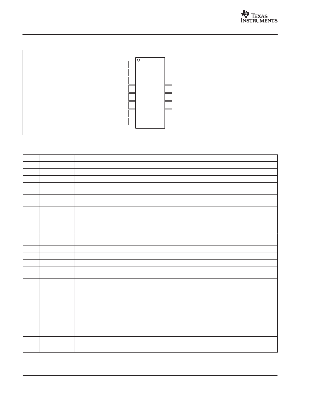
PIN CONFIGURATION
www.ti.com
Top View
V
GND
V
V
V
V
V
V
EXC
OUT
1
2
A
3
SA
4
IN1
IN2
FB
PGA309
5
6
7
8
SJ
16
15
14
13
12
11
10
9
REFIN/REF
TEMP
IN
SDA
SCL
PRG
GND
D
V
SD
TEST
OUT
PIN DESCRIPTION
PIN
NAME DESCRIPTION
1 V
EXC
2 GND
3 V
4 V
5 V
6 V
7 V
8 V
A
SA
IN1
IN2
FB
OUT
SJ
9 TEST Test/External Controller Mode pin. Pull to GNDD in normal mode.
10 V
SD
11 GND
D
12 PRG Single-wire interface program pin. UART-type interface for digital calibration of the PGA309 over a single wire. Can be
13 SCL Clock input/output for Two-Wire, industry-standard compatible interface for reading and writing digital calibration and
14 SDA Data input/output for Two-Wire, industry-standard compatible interface for reading and writing digital calibration and
15 TEMP
16 REFIN/REF
IN
OUT
Bridge sensor excitation. Connect to bridge if linearization and/or internal reference for bridge excitation is to be used.
Analog ground. Connect to analog ground return path for VSA. Should be same as GNDD.
Analog voltage supply. Connect to analog voltage supply. To be within 200mV of VSD.
Signal input voltage 1. Connect to + or – output of sensor bridge. Internal multiplexer can change connection internally to
Front-End PGA.
Signal input voltage 2. Connect to + or – output of sensor bridge. Internal multiplexer can change connection internally to
Front-End PGA.
V
feedback pin. Voltage feedback sense point for over/under-scale limit circuitry. When internal gain set resistors for the
OUT
output amplifier are used, this is also the voltage feedback sense point for the output amplifier. VFB in combination with V
allows for ease of external filter and protection circuits without degrading the PGA309 V
connected to either V
or the point of feedback for V
OUT
, if external protection is used.
OUT
accuracy. VFB must always be
OUT
Analog output voltage of conditioned sensor.
Output amplifier summing junction. Use for output amplifier compensation when driving large capacitive loads
(> 100pF) and/or for using external gain setting resistors for the output amplifier.
Digital voltage supply. Connect to digital voltage supply. To be within 200mV of VSA.
Digital ground. Connect to digital ground return path for VSD. Should be same as GNDA.
connected to V
for a three-lead (VS, GND, V
OUT
) digitally-programmable sensor assembly.
OUT
configuration from external EEPROM. Can also communicate directly to the registers in the PGA309 through the Two-Wire,
industry-standard compatible interface.
configuration from external EEPROM. Can also communicate directly to the registers in the PGA309 through the Two-Wire,
industry-standard compatible interface.
External temperature signal input. PGA309 can be configured to read a bridge current sense resistor as an indicator of bridge
temperature, or an external temperature sensing device such as diode junction, RTD, or thermistor. This input can be internally
gained by 1, 2, 4, or 8. In addition, this input can be read differentially with respect to V
V
. There is also an internal, register-selectable, 7µA current source (I
REF
thermistor, or diode excitation source.
) that can be connected to TEMPIN as an RTD,
TEMP
GNDA
, V
, or the internal/external
EXC
Reference input/output pin. As an output, the internal reference (selectable as 2.5V or 4.096V) is available for system use on
this pin. As an input, the internal reference may be disabled and an external reference can then be applied as the reference for
the PGA309.
TSSOP
SJ
8
www.ti.com
V
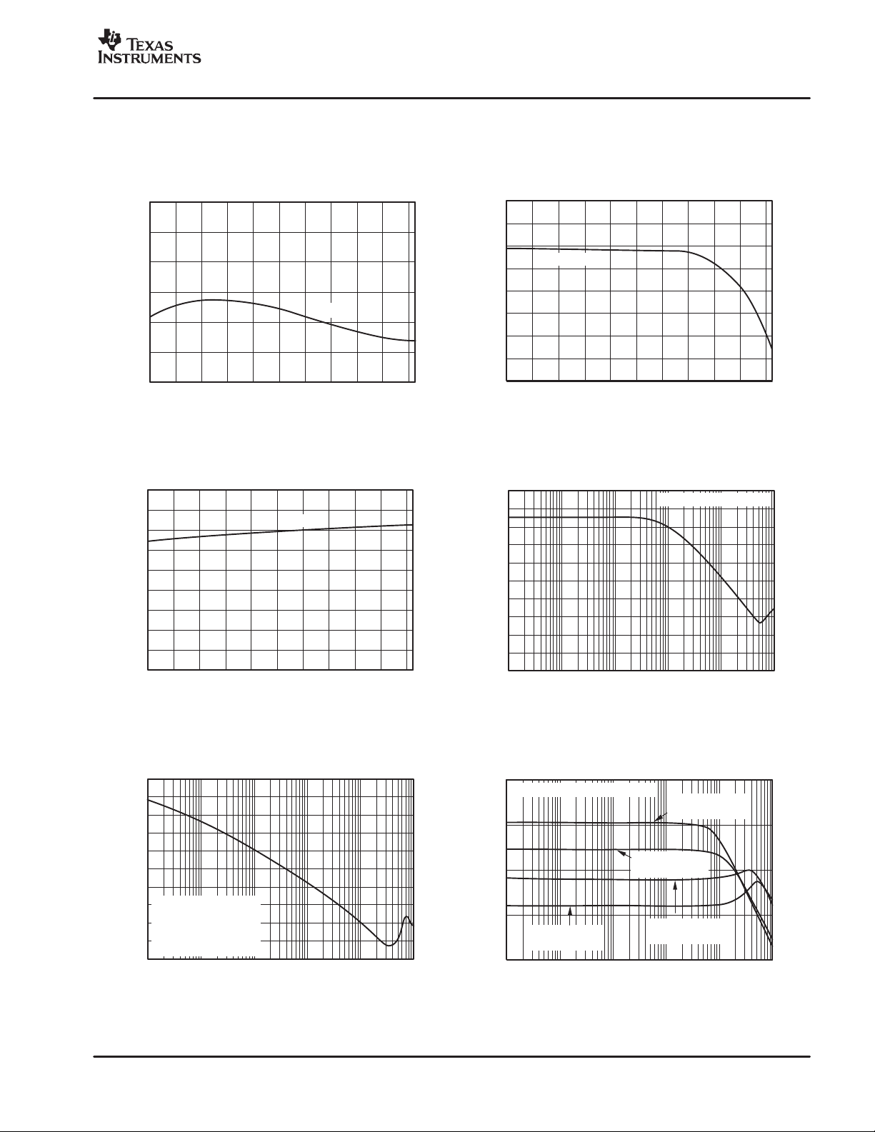
vs TEMPERATURE
IBCURRENT vs TEMPERATURE
I
CURRENT vs TEMPERATURE
COMMON−MODE REJECTION RATIO vs FREQUENCY
POWER−SUPPLY REJECTION RATIO vs FREQUENCY
CLOSED−LOOP GAIN vs FREQUENCY
TYPICAL CHARACTERISTICS
TA = +25°C, VSA = VSD = +5V (VSA = V
unless otherwise noted.
SUPPLY ANALOG
, VSD = V
SUPPLY DIGITAL
SBOS292A − DECEMBER 2003 − REVISED AUGUST 2004
, VSA must equal VSD), GNDD = GNDA = 0, and V
= REFIN/REF
REF
"#$%
= +5V ,
OUT
(V)
V
REF
4.090
4.085
4.080
4.075
4.070
4.065
4.060
−55−35−
9
8
7
6
A)
µ
5
(
4
TEMP
I
3
2
1
0
−55−35−
REF
Average
15 5 25 45 65 85 105 125 145
Temperature (_C)
TEMP
Average
15 5 25 45 65 85 105 125 145
Temperature (_C)
1.0
0.5
0
−
(nA)
−
B
I
−
−
−
−
0.5
1.0
1.5
2.0
2.5
3.0
−55−35−
Average,nA
15 5 25 45 65 85 105 125 145
Temperature (_C)
70
60
RTO of Front−End PGA
50
40
30
20
10
CMRR (dB)
0
−
10
−
20
−
30
10 100 1k 10k 100k 1M
Frequency (Hz)
90
80
70
60
50
40
PSRR (dB)
30
Small−Signal
20
V
and V
=2.5V
EXT
OUT
Enabled
−
10
0
10
REF
V
REF
PSRR at V
10 100 1k 10k 100k 1M
Frequency (Hz)
80
G
= Output Amplifer Gain
OUTAMP
60
40
G
OUTAMP
G
FRONT
G
OUTAMP
G
FRONT
=9V/V
= 32V/V
=9V/V
= 128V/V
Gain (dB)
20
G
OUTAMP
G
FRONT
=2V/V
=8V/V
G
OUTAMP
G
FRONT
=2V/V
=32V/V
0
10 100 1k 10k 100k 1M
Frequency (Hz)
9

"#$%
V
SWINGTORAILvsI
IQvs TEMPERATURE
TEMPERATURE ADC ERROR (INTERNAL MODE)
TEMPERATURE ADC ERROR (EXTERNAL MODES)
SBOS292A − DECEMBER 2003 − REVISED AUGUST 2004
TYPICAL CHARACTERISTICS (Cont.)
TA = +25°C, VSA = VSD = +5V (VSA = V
unless otherwise noted.
SUPPLY ANALOG
, VSD = V
SUPPLY DIGITAL
, VSA must equal VSD), GNDD = GNDA = 0, and V
= REFIN/REF
REF
www.ti.com
OUT
= +5V ,
V
S
V
S
V
S
V
S
V
S
C)
_
Temp ADC Error(
V
S
−
0.1
−
0.2
−
0.3
−
0.4
−
0.5
0.5
0.4
0.3
0.2
0.1
0
0.4
0.2
0
−
0.2
−
0.4
−
0.6
−
0.8
−
1.0
−
1.2
−55−35−
0
OUT
VS=2.7V
LOAD
VS=5V
VS=5V
VS=2.7V
5 10152025
I
(mA)
LOAD
15 5 25 45 65 85 105 125 145
Actual Die Temperature (_C)
1.6
1.4
1.2
All Blocks Enabled
1.0
0.8
(mA)
Q
I
0.6
Ref, Exc, and ADC Disabled
0.4
0.2
0
−55−35−
15 5 25 45 65 85 105 125 145
Temperature (_C)
0.4
0.3
0.2
Reg 6 = 0433h
V
= 2.5VInternal
REF
15−Bit+ Sign
Reg6 = 0503h
V
REF
(Temp ADC Internal)
15−Bit + Sign
0.1
0
−
TotalError (% ofFS)
−
−
−
Reg 6 = 0430h
0.1
V
= 2.5V Internal
REF
0.2
0.3
11−Bit + Sign
Reg 6 = 0403h
V
=5VExternal
REF
15−Bit + Sign
0.4
−
100−80−60−40−20 0 20 40 60 80 100
Input Signal(% FS of V
REF
)
=2.048V
V
NOISE
REF
(0.1Hz TO 10Hz)
V/div
µ
50
Measured After Bandpass Filter
0.1Hz Second−Order High−Pass
10Hz Fourth−Order Low−Pass
1s/div
10
V
REF
= 4.096V
(0.1Hz TO 10Hz PEAK−TO−PEAK NOISE)
=+61mV
V
IN
CLK_CFG= 00 (default)
1mV/div
Measured After Bandpass Filter
0.1Hz Second−Order High−Pass
10Hz Fourth−Order Low−Pass
V
NOISE
OUT
Coarse Offset =−59mV
1s/div
G=1152

www.ti.com
LARGE−SIGNAL STEP RESPONSE
LARGE−SIGNAL STEP RESPONSE
SMALL−SIGNAL STEP RESPONSE
SMALL−SIGNAL STEP RESPONSE
CAPACITIVE LOAD DRIVE
OVERVOLTAGE RECOVERY
TYPICAL CHARACTERISTICS (Cont.)
TA = +25°C, VSA = VSD = +5V (VSA = V
unless otherwise noted.
SUPPLY ANALOG
, VSD = V
SUPPLY DIGITAL
SBOS292A − DECEMBER 2003 − REVISED AUGUST 2004
, VSA must equal VSD), GNDD = GNDA = 0, and V
= REFIN/REF
REF
"#$%
= +5V ,
OUT
Gain = 8
(500mV/div)
OUT
V
Time (10µs/div)
(500mV/div)
OUT
V
Time (10µs/div)
Gain = 8
(50mV/div)
OUT
V
(50mV/div)
OUT
V
Gain = 1152
Gain = 256
Time (10µs/div)
25
G
20
s)
µ
15
G
=9V/V
OUTAMP
10
0.5% Settling Time (
5
G
0
0 500 1000 1500 2000 2500
C
(pF)
LOAD
OUTAMP
OUTAMP
=2V/V
=3.6V/V
Time (10µs/div)
V
OUT
(1V/div)
OUT
V
IN
(200mV/div),V
IN
V
Time (100µs/div)
11

"#$%
SBOS292A − DECEMBER 2003 − REVISED AUGUST 2004
TYPICAL CHARACTERISTICS (Cont.)
TA = +25°C, VSA = VSD = +5V (VSA = V
unless otherwise noted.
SUPPLY ANALOG
, VSD = V
SUPPLY DIGITAL
, VSA must equal VSD), GNDD = GNDA = 0, and V
= REFIN/REF
REF
www.ti.com
OUT
= +5V ,
120
100
80
(dB)
60
OL
A
40
20
0
OPEN−LOOP GAIN/PHASE vs FREQUENCY
110100
OUTPUT AMPLIFIER
10k 100k 1M 10M0.1
1k
Frequency (Hz)
Error (LSB)
−
−
−
20
15
10
−
10
15
20
5
0
5
CL=100pF
=4.7k
R
L
45
Ω
0
−
45
)
_
−
90
Phase (
−
135
−
180
−
225
GAIN DAC TYPICAL ERROR vs CODE
Code (LSB)
20
15
10
5
0
Error(LSB)
−
5
−
10
−
15
−
20
ZERO DAC TYPICAL ERROR vs CODE
Unit 2
Unit 1
7000010000 20000 30000 4 0000 60000500000
Code (LSB)
7000010000 20000 30000 4 0000 60000500000
12

www.ti.com
"#$%
SBOS292A − DECEMBER 2003 − REVISED AUGUST 2004
FUNCTIONAL DESCRIPTION
The PGA309 is a programmable analog signal
conditioner designed for resistive bridge sensor
applications. It is a complete signal conditioner with
bridge excitation, initial span and offset adjustment,
temperature adjustment of span and offset,
internal/external temperature measurement capability,
output over-scale and under-scale limiting, fault
detection, and digital calibration. The PGA309, in a
calibrated sensor module, can reduce errors to the level
approaching the bridge sensor repeatability. Figure 1
shows a block diagram of the PGA309. Following is a
brief overview of each major function.
SENSOR ERROR ADJUSTMENT RANGE
The adjustment capability of the PGA309 is
summarized in Table 1.
FSS (full-scale sensitivity) 1mV/V to 245mV/V
Span TC Over ±3300ppmFS/°C
Span TC nonlinearity > 10%
Zero offset ±200%FS
Zero offset TC Over ±3000ppmFS/°C
Zero offset TC nonlinearity > 10%
Sensor impedance Down to 200Ω
(1)
Depends on the temperature sensing scheme
(2)
Combined coarse and fine offset adjust
(3)
Lower impedance possible by using a dropping resistor in series with the
bridge
(2)
Table 1. PGA309 Adjustment Capability
GAIN SCALING
The core of the PGA309 is the precision low-drift and no
1/f noise Front-End PGA. The overall gain of the
Front-End PGA + Output Amplifier can be adjusted
from 2.7V/V to 1152V/V. The polarity of the inputs can
be switched through the 2x2 input mux to accommodate
sensors with unknown polarity output.
The Front-End PGA provides initial coarse signal gain
using a no 1/f noise, auto-zero instrumentation
amplifier. The fine gain adjust is accomplished by the
16-bit attenuating Gain Digital-to-Analog Converter
(Gain DAC). This Gain DAC is controlled by the data in
the Temperature Compensation Lookup Table driven by
the Temperature Analog-to-Digital Converter (Temp
ADC). In order to compensate for second-order and
higher drift nonlinearity, the span drift can be fitted to
(1)
(2)
(3)
piecewise linear curves during calibration with the
coefficients stored in an external nonvolatile EEPROM
lookup table.
Following the fine gain adjust stage is the Output
Amplifier that provides additional programmable gain.
Two key output amplifier connections, VFB and VSJ, are
brought out on the PGA309 for application flexibility.
These connections allow for an accurate conditioned
signal voltage while also providing a means for PGA309
output overvoltage and large capacitive loading for
RFI/EMI filtering required in many end applications.
OFFSET ADJUSTMENT
The sensor offset adjustment is performed in two
stages. The input-referred Coarse Offset Adjust DAC
has approximately a ±60mV offset adjustment range for
a selected V
of 5 V. The fine offset and the offset drift
REF
are canceled by the 16-bit Zero DAC that sums the
signal with the output of the front-end instrumentation
amplifier. Similar to the Gain DAC, the input digital
values of the Zero DAC are controlled by the data in the
Temperature Compensation Lookup Table, stored in
external EEPROM, driven by the Temp ADC. The
programming range of the Zero DAC is 0V to V
REF
with
an output range of 0.1V to VSA − 0.1V.
VOLTAGE REFERENCE
The PGA309 contains a precision low-drift voltage
reference (selectable for 2.5V or 4.096V) that can be
used for external circuitry through the REFIN/REF
OUT
pin. This same reference is used for the Coarse Offset
Adjust DAC, Zero DAC, Over/Under-Scale Limits and
sensor excitation/linearization through the V
EXC
pin.
When the internal reference is disabled, the
REFIN/REF
pin should be connected to an external
OUT
reference or to VSA for ratiometric-scaled systems.
SENSOR EXCITATION AND LINEARIZATION
A dedicated circuit with a 7-bit + sign DAC for sensor
voltage excitation and linearization is provided on the
PGA309. This block scales the reference voltage and
sums it with a portion of the PGA309 output to
compensate the positive or negative bow-shaped
nonlinearity exhibited by many sensors over their
applied pressure range. Sensors not requiring
linearization can be connected directly to the supply
(VSA) or to the V
pin with the Linearization DAC (Lin
EXC
DAC) set to zero.
13

"#$%
SBOS292A − DECEMBER 2003 − REVISED AUGUST 2004
www.ti.com
+5V
Bridge
Sensor
R
TEMP
V
TEMP
TEST
EXC
V
IN1
V
IN2
IN
PGA309
Σ
V
OUT
Temp AD C
Signals Mux
2x2 Multiplexer
K
LIN
Internal
Temp Se nse
Coarse
Offset Adjust
V
Front−EndP GA
(Gain 4 to 1 28)
Fault Conditions
Monitoring Circuit
Test Logic
K
REF
Linearization
OS
V
REF
DAC
Temperature ADC
Input Select
Front−End
PGA Out
Fault
Out
V
V
Power−On
Reset
V
FB
V
TEMP
Temperature
SpanTC and OffsetTC A djust Lookup
Table with interp olation
Fine Offset
Fine Gain
Adjust
SD
ADC
Adjust
Gain
DAC
SA
Zero
DAC
REFIN/REF
Interface and Control
OUT
Band−Gap
Volta ge
Reference
Circuitry
Over/Under−
Scale Limits
V
OUT
Fault Out
Output
Amp
Int/Ext
Feedback
Output Coarse
Gain Adjust
(2 to 9)
+5V
SDA
SCL
Two−Wire
EEPROM
(SOT23−5)
PRG
V
OUT FILT
R
ISO
100
R
100
C
F
150pF
Ω
C
L
10nF
FB
Ω
V
OUT
V
FB
V
FB
V
SJ
GND
A
GND
D
Figure 1. Simplified Diagram of the PGA309 in a Typical Configuration.
14

www.ti.com
"#$%
SBOS292A − DECEMBER 2003 − REVISED AUGUST 2004
ADC FOR TEMPERATURE SENSING
The temperature sense circuitry drives the
compensation for the sensor span and offset drift.
Either internal or external temperature sensing is
possible. The temperature can be sensed in one of the
following ways:
D Bridge impedance change (excitation current
sense, in the positive or negative part of the bridge),
for sensors with large temperature coefficient of
resistance (TCR > 0.1%/°C).
D On-chip PGA309 temperature, when the chip is
located sufficiently close to the sensor.
D External diode, thermistor, or RTD placed on the
sensor membrane. An internal 7µA current source
may be enabled to excite these types of
temperature sensors.
The temperature signal is digitized by the onboard
Temp ADC. The output of the T emp ADC is used by the
control digital circuit to read the data from the Lookup
Table in an external EEPROM, and set the output of the
Gain DAC and the Zero DAC to the calibrated values as
temperature changes.
An additional function provided through the Temp ADC
is the ability to read the V
ADC input mux. This provides flexibility for a digital
output through either One-Wire or Two-Wire interface,
as well as the possibility for an external microcontroller
to perform real-time custom calibration of the PGA309.
EXTERNAL EEPROM AND TEMPERATURE
COEFFICIENTS
The PGA309 uses an industry-standard Two-Wire
external EEPROM (typically, a SOT23-5 package). A
1k-bit (minimum) EEPROM is needed when using all 17
temperature coefficients. Larger EEPROMs may be
used to provide space for a serial number, lot code, or
other data.
The first part of the external EEPROM contains the
configuration data for the PGA309, with settings for:
pin back through the Temp
OUT
D Register 3—Reference Control and Linearization
D Register 4—PGA Coarse Offset and Gain/Output
Amplifier Gain
D Register 5—PGA Configuration and Over/Under-
Scale Limit
D Register 6—Temp ADC Control
This section of the EEPROM contains its own individual
checksum (Checksum1).
The second part of the external EEPROM contains up
to 17 temperature index values and corresponding
temperature coefficients for the Zero DAC and Gain
DAC adjustments with measured temperature, and
also contains its own checksum (Checksum2).
The PGA309 lookup logic contains a linear interpolation
algorithm for accurate DAC adjustments between
stored temperature indexes. This approach allows for
a piecewise linear temperature compensation of up to
17 temperature indexes and associated temperature
coefficients.
If either Checksum1, Checksum2, or both are incorrect,
the output of the PGA309 is set to high-impedance.
FAULT MONITOR
To detect sensor burnout or a short, a set of four
comparators are connected to the inputs of the
Front-End PGA. If any of the inputs are taken to within
100mV of ground or V
the Front-End PGA, then the corresponding
comparator sets a sensor fault flag that causes the
PGA309 V
or ground, depending upon the alarm configuration
setting (Register 5—PGA Configuration and
Over/Under-Scale Limit). This will be well above the set
Over-Scale Limit level or well below the set
Under-Scale Limit level. The state of the fault condition
can be read in digital form in Register 8—Alarm Status
Register. If the Over/Under-Scale Limit is disabled, the
PGA309 output voltage will still be driven within 100mV
of either V
configuration setting.
There are five other fault detect comparators that help
detect subtle PGA309 front-end violations that could
otherwise result in linear voltages at V
interpreted as valid states. These are especially useful
during factory calibration and setup, and are configured
through Register 5—PGA Configuration and
Over/Under-Scale Limit. Their status can also be read
back through Register 8—Alarm Status Register.
OVER-SCALE AND UNDER-SCALE LIMITS
The over-scale and under-scale limit circuitry combined
with the fault monitor circuitry provides a means for
system diagnostics. A typical sensor-conditioned
output may be scaled for 10% to 90% of the system
ADC range for the sensor normal operating range. If the
conditioned pressure sensor is below 4%, it is
considered under-pressure; if over 96%, it is
considered over-pressure.
The PGA309 over/under-scale limit circuit can be
programmed individually for under-scale and
over-scale values that clip or limit the PGA309 output.
From a system diagnostic view, 10% to 90% of ADC
range is normal operation, < 4% is under-pressure, and
> 96% is over-pressure. If the fault detect circuitry is
used, a detected fault will cause the PGA309 output to
be driven to positive or negative saturation. If this fault
to be driven within 100mV of either V
OUT
or ground, depending upon the alarm
SA
or violate the input CMR of
EXC,
that would be
OUT
SA
15

"#$%
SBOS292A − DECEMBER 2003 − REVISED AUGUST 2004
www.ti.com
flag is programmed for high, then > 97% ADC range will
be a fault; if programmed for low, then < 3% ADC range
will be a fault. In this configuration, the system software
can be used to distinguish between over- or
under-pressure condition, which indicates an
out-of-control process, or a sensor fault.
POWER-UP AND NORMAL OPERATION
The PGA309 has circuitry to detect when the power
supply is applied to the PGA309, and reset the internal
registers and circuitry to an initial state. This reset also
occurs when the supply is detected to be invalid, so that
the PGA309 is in a known state when the supply
becomes valid again. The rising threshold for this circuit
is typically 2.2V and the falling threshold is typically
1.7V. After the power supply becomes valid, the
PGA309 waits for approximately 25ms and then
attempts to read the configuration data from the
external EEPROM device.
If the EEPROM has the proper flag set in address
locations 0 and 1, then the PGA309 continues reading
the first part of the EEPROM; otherwise, the PGA309
waits for one second before trying again. If the PGA309
detects no response from the EEPROM, the PGA309
waits for one second and tries again; otherwise, the
PGA309 tries to free the bus and waits for 25ms before
trying to read the EEPROM again. If a successful read
of the first part of the EEPROM is accomplished,
(including valid Checksum1 data), the PGA309 triggers
the Temp ADC to measure temperature. For 16-bit
resolution results, the converter takes approximately
125ms to complete a conversion. Once the conversion
is complete, the PGA309 begins reading the Lookup
Table information from the EEPROM (second part) to
calculate the settings for the Gain DAC and Zero DAC.
The PGA309 reads the entire Lookup Table so that it
can determine if the checksum for the Lookup Table
(Checksum2) is correct. Each entry in the Lookup Table
requires approximately 500µs to read from the
EEPROM. Once the checksum is determined to be
valid, the calculated values for the Gain and Zero DACs
are updated into their respective registers, and the
output amplifier is enabled. The PGA309 then begins
looping through this entire procedure, starting with
reading the EEPROM configuration registers from the
first part of the EEPROM, then starting a new
conversion on the Temp ADC, which then triggers
reading the Lookup Table data from the second part of
the EEPROM. This loop continues indefinitely.
DIGITAL INTERFACE
There are two digital interfaces on the PGA309. The
PRG pin uses a One-Wire, UART-compatible interface
with bit rates from 4.8Kbits/s to 38.4Kbits/s. The SDA
and SCL pins together form an industry standard
Two-Wire interface at clock rates from 1kHz to 400kHz.
The external EEPROM uses the Two-Wire interface.
Communication to the PGA309 internal registers, as
well as to the external EEPROM, for programming and
readback can be conducted through either digital
interface.
It is also possible to connect the One-Wire
communication pin, PRG, to the V
pin in true
OUT
three-wire sensor modules and still allow for
programming. In this mode, the PGA309 output
amplifier may be enabled for a set time period and then
disabled again to allow sharing of the PRG pin with the
V
connection. This allows for both digital calibration
OUT
and analog readback during sensor calibration in a
three-wire sensor module.
The Two-Wire interface has timeout mechanisms to
prevent bus lockup from occurring. The Two-Wire
master controller in the PGA309 has a mode that
attempts to free up a stuck-at-zero SDA line by issuing
SCL pulses, even when the bus is not indicated as idle
after a timeout period has expired. The timeout will only
apply when the master portion of the PGA309 is
attempting to initiate a Two-Wire communication.
16

www.ti.com
DETAILED BLOCK DIAGRAM
"#$%
SBOS292A − DECEMBER 2003 − REVISED AUGUST 2004
V
TEMP
TEST
REFIN/REF
OUT
V
V
SA
SD
16 3 10
Linearizationand V
7−Bit + Sign
LinDAC
Temp ADC
Internal REF
Temp Select
Coarse
Offset Adjust
4−Bit + Sign
Gain Adjust
Source
DAC
PGA309
V
Enable
V
EXC
EXC
1
V
SA
I
TEMP
7µA
IN
TEMP
15
V
REF
V
EXC
V
OUT
V
IN2
EXC
I
Enable
TEMP
IN
Temp ADC
Input Mux
Temp ADC Input
Mux Select
PGA Gain Select(1 of 8)
Rangeof 4 to 128
(withPGADiffAmpGain=4)
Input Mux
Control
Σ
Internal
Temp Sense
xG
Temp ADC, PGA
(x1,x2, x4, x8)
V
V
INP
REF
5
V
V
IN1
4
Input Mux
INN
Fault Monitor
Test Logic
9
R
Circuit
15−Bit+ Sign
Temp ADC
V
REF
A2
Auto
Zero
R
G
R
Auto
Zero
EXC
Temp ADC
Ref Mux
REFT
V
FB
Temp ADC
REF Select
x0.83
x0.52
V
REF
V
EXC
V
SA
V
REF
(2.5V or 4.096V)
x0.166
x0.124
V
Control Registers
Alarm Register
Offset TC Adjust and Scan TC Adjust
Look−Up Logic with Interpolation Algorithm
Fine
Offset Adjust
16−Bit
Zero
DAC
4R
R
Front−End
F
F
Front End PGA
A1
R
PGA
Diff Amp
Auto
Zero
R
PGA Output
INT/EXT FB Select
Alarm Register Inputs
Output Gain Select (1 of 7)
Range of 2 to 9
V
Internal Set
Digital Controls
A3
V
SA
POR
V
Internal Set
REF
(2.5V or 4.096V)
REF
Interface and
ControlCircuitry
Fine Gain Adjust
(16−Bit)
16−Bit
Gain
DAC
Bandgap
Reference
R
SET
RGO
V
V
REF
RFO
V
REF
SD
Amplifier
Over−Scale
Limit
3−Bit
DAC
Output
3−Bit
DAC
Under−Scale
Limit
Scale
Limiter
VFBV
OUT
14
13
12
7
6
SDA
SCL
PRG
V
OUT
V
V
FB
SJ
8
112
GNDAGND
D
Figure 2. Detailed Block Diagram
17

PACKAGE OPTION ADDENDUM
www.ti.com
9-Dec-2004
PACKAGING INFORMATION
Orderable Device Status
(1)
Package
Type
Package
Drawing
Pins Package
Qty
Eco Plan
PGA309AIPWR ACTIVE TSSOP PW 16 2500 Green (RoHS &
no Sb/Br)
PGA309AIPWT ACTIVE TSSOP PW 16 250 Green (RoHS &
no Sb/Br)
(1)
The marketing status values are defined as follows:
ACTIVE: Product device recommended for new designs.
LIFEBUY: TI has announced that the device will be discontinued, and a lifetime-buy period is in effect.
NRND: Not recommended for new designs. Device is in production to support existing customers, but TI does not recommend using this part in
a new design.
PREVIEW: Device has been announced but is not in production. Samples may or may not be available.
OBSOLETE: TI has discontinued the production of the device.
(2)
Eco Plan - May not be currently available - please check http://www.ti.com/productcontent for the latest availability information and additional
product content details.
None: Not yet available Lead (Pb-Free).
Pb-Free (RoHS): TI's terms "Lead-Free" or "Pb-Free" mean semiconductor products that are compatible with the current RoHS requirements
for all 6 substances, including the requirement that lead not exceed 0.1% by weight in homogeneous materials. Where designed to be soldered
at high temperatures, TI Pb-Free products are suitable for use in specified lead-free processes.
Green (RoHS & no Sb/Br): TI defines "Green" to mean "Pb-Free" and in addition, uses package materials that do not contain halogens,
including bromine (Br) or antimony (Sb) above 0.1% of total product weight.
(3)
MSL, Peak Temp. -- The Moisture Sensitivity Level rating according to the JEDECindustry standard classifications, and peak solder
temperature.
(2)
Lead/Ball Finish MSL Peak Temp
CU SNPB Level-1-260C-UNLIM
CU SNPB Level-1-260C-UNLIM
(3)
Important Information and Disclaimer:The information provided on this page represents TI's knowledge and belief as of the date that it is
provided. TI bases its knowledge and belief on information provided by third parties, and makes no representation or warranty as to the
accuracy of such information. Efforts are underway to better integrate information from third parties. TI has taken and continues to take
reasonable steps to provide representative and accurate information but may not have conducted destructive testing or chemical analysis on
incoming materials and chemicals. TI and TI suppliers consider certain information to be proprietary, and thus CAS numbers and other limited
information may not be available for release.
In no event shall TI's liability arising out of such information exceed the total purchase price of the TI part(s) at issue in this document sold by TI
to Customer on an annual basis.
Addendum-Page 1

MECHANICAL DATA
MTSS001C – JANUARY 1995 – REVISED FEBRUARY 1999
PW (R-PDSO-G**) PLASTIC SMALL-OUTLINE PACKAGE
14 PINS SHOWN
0,65
1,20 MAX
14
0,30
0,19
8
4,50
4,30
PINS **
7
Seating Plane
0,15
0,05
8
1
A
DIM
14
0,10
6,60
6,20
M
0,10
0,15 NOM
2016
0°–8°
Gage Plane
24
0,25
0,75
0,50
28
A MAX
A MIN
NOTES: A. All linear dimensions are in millimeters.
B. This drawing is subject to change without notice.
C. Body dimensions do not include mold flash or protrusion not to exceed 0,15.
D. Falls within JEDEC MO-153
3,10
2,90
5,10
4,90
5,10
4,90
6,60
6,40
7,90
7,70
9,80
9,60
4040064/F 01/97
POST OFFICE BOX 655303 • DALLAS, TEXAS 75265

IMPORTANT NOTICE
Texas Instruments Incorporated and its subsidiaries (TI) reserve the right to make corrections, modifications,
enhancements, improvements, and other changes to its products and services at any time and to discontinue
any product or service without notice. Customers should obtain the latest relevant information before placing
orders and should verify that such information is current and complete. All products are sold subject to TI’s terms
and conditions of sale supplied at the time of order acknowledgment.
TI warrants performance of its hardware products to the specifications applicable at the time of sale in
accordance with TI’s standard warranty. Testing and other quality control techniques are used to the extent TI
deems necessary to support this warranty . Except where mandated by government requirements, testing of all
parameters of each product is not necessarily performed.
TI assumes no liability for applications assistance or customer product design. Customers are responsible for
their products and applications using TI components. To minimize the risks associated with customer products
and applications, customers should provide adequate design and operating safeguards.
TI does not warrant or represent that any license, either express or implied, is granted under any TI patent right,
copyright, mask work right, or other TI intellectual property right relating to any combination, machine, or process
in which TI products or services are used. Information published by TI regarding third-party products or services
does not constitute a license from TI to use such products or services or a warranty or endorsement thereof.
Use of such information may require a license from a third party under the patents or other intellectual property
of the third party, or a license from TI under the patents or other intellectual property of TI.
Reproduction of information in TI data books or data sheets is permissible only if reproduction is without
alteration and is accompanied by all associated warranties, conditions, limitations, and notices. Reproduction
of this information with alteration is an unfair and deceptive business practice. TI is not responsible or liable for
such altered documentation.
Resale of TI products or services with statements different from or beyond the parameters stated by TI for that
product or service voids all express and any implied warranties for the associated TI product or service and
is an unfair and deceptive business practice. TI is not responsible or liable for any such statements.
Following are URLs where you can obtain information on other Texas Instruments products and application
solutions:
Products Applications
Amplifiers amplifier.ti.com Audio www.ti.com/audio
Data Converters dataconverter.ti.com Automotive www.ti.com/automotive
DSP dsp.ti.com Broadband www.ti.com/broadband
Interface interface.ti.com Digital Control www.ti.com/digitalcontrol
Logic logic.ti.com Military www.ti.com/military
Power Mgmt power.ti.com Optical Networking www.ti.com/opticalnetwork
Microcontrollers microcontroller.ti.com Security www.ti.com/security
Telephony www.ti.com/telephony
Video & Imaging www.ti.com/video
Wireless www.ti.com/wireless
Mailing Address: Texas Instruments
Post Office Box 655303 Dallas, Texas 75265
Copyright 2004, Texas Instruments Incorporated
 Loading...