

Page 1

User's Guide
SBAU124 – December 2006
PCM4222EVM User's Guide
This document serves as a reference for the PCM4222EVM evaluation module. When
used in conjunction with commonly available audio test equipment, the PCM4222EVM
provides a complete environment for evaluating the functionality and performance of
the PCM4222 integrated circuit. Indirectly, the PCM4222EVM serves as an evaluation
platform for the PCM4220 integrated circuit; the PCM4220 is a subset derivative of the
PCM4222 device.
This document includes information regarding absolute operating conditions,
power-supply requirements, and hardware configuration for the evaluation module. The
electrical schematics and bill of materials are also included for reference purposes.
Throughout this document, the acronym EVM and the phrase evaluation module are
synonymous with the PCM4222EVM.
Contents
1 Introduction .......................................................................................... 3
2 Hardware Configuration ............................................................................ 6
3 Hardware Reference .............................................................................. 16
List of Figures
1 PCM4222 Functional Block Diagram ............................................................ 3
2 Simplified Block Diagram for the PCM4222EVM Evaluation Module ........................ 5
3 Power Supply Jumper Configuration ............................................................. 7
4 PCM4222EVM Schematics, Page 1 of 2 ...................................................... 17
5 PCM4222EVM Schematics, Page 2 of 2 ...................................................... 18
List of Tables
1 Absolute Operating Conditions ................................................................... 6
2 Recommended Power Supply Range............................................................ 7
3 Master Clock Source Selection ................................................................... 9
4 Master Clock Frequencies for Common Output Sampling and Data Rates ................ 9
5 PCM Output Mode Configuration ............................................................... 10
6 PCM Sampling Mode Selection ................................................................. 10
7 Audio Serial Port Header Configuration ........................................................ 11
8 Audio Serial Port Slave/Master Mode Selection .............................................. 11
9 Audio Serial Port Data Format Selection ...................................................... 11
10 TDM Sub-frame Assignment .................................................................... 12
11 PCM Output Word Length Selection ........................................................... 12
12 Digital Decimation Filter Configuration ......................................................... 12
13 Digital High-Pass Filter Switch Operation ...................................................... 13
14 DIT4192 Serial Data and Clock Enable Operation ........................................... 13
15 DIT4192 Master Clock Divider Configuration .................................................. 13
16 DIT4192 Data Format Selection ................................................................ 14
17 DIT4192 Transmission Mode Configuration ................................................... 14
18 DSD Data Port Header Pin Configuration ..................................................... 15
SBAU124 – December 2006 PCM4222EVM User's Guide 1
Submit Documentation Feedback
Page 2

www.ti.com
19 DSD Output Mode Configuration ................................................................ 15
20 DSD Output Rate Selection ...................................................................... 15
21 Modulator Data Port Header Pin Configuration ............................................... 16
22 Multi-Bit Modulator (MBM) Output Mode Configuration ...................................... 16
23 Bill of Materials .................................................................................... 19
2 PCM4222EVM User's Guide SBAU124 – December 2006
Submit Documentation Feedback
Page 3
www.ti.com
Reference
Multi-Bit
Delta-Sigma
Multi-Bit
Delta-Sigma
Digital
Filters
Audio
Serial
Port
DSD
Engine
Reset
Logic
Control
and
Status
MasterClock
andTiming
VINL+
VCOML
REFGNDL
VREFL
S/M
FMT0
FMT1
OWL0
OWL1
SUB0(WCK0)
SUB1(MCK0)
PCMEN
FS0(MOD3)
FS1(MOD4)
OVFL
OVFR
MODEN
DSDEN(MOD6)
DSDCLK
DSDL
DSDR
DSDMODE
VCC1
VCC2
AGND
AGND
AGND
AGND
AGND
AGND
DGND
DGND
DGND
VDD
RST
LRCK
BCK
DATA
DF(MOD5)
HPFDR(MOD1)
HPFDL(MOD2)
VREFR
MCKI
REFGNDR
VCOMR
VINL-
VINR+
VINR-
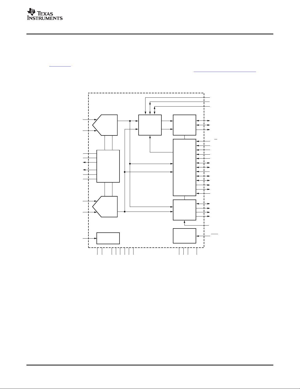
Introduction
1 Introduction
The PCM4222EVM evaluation module from Texas Instruments provides a convenient platform for testing
the PCM4222 , a high-performance, stereo audio analog-to-digital (A/D) converter integrated circuit.
Figure 1 shows a block diagram of the PCM4222 device. Refer to the PCM4222 product datasheet for
additional information and details regarding this product. The PCM4222EVM evaluation module includes
analog input and digital output circuitry with common audio connectors, providing a direct interface to
audio test systems for measurement and evaluation.
Figure 1. PCM4222 Functional Block Diagram
SBAU124 – December 2006 PCM4222EVM User's Guide 3
Submit Documentation Feedback
Page 4

www.ti.com
Introduction
The primary features of the PCM4222EVM include:
• Simple configuration using switches and power-supply jumpers.
• Two differential input buffer/filter circuits employing the Texas Instruments OPA1632 fully differential
amplifer integrated circuit.
• Two Texas Instruments DIT4192 digital audio interface transmitters, providing AES3-encoded output
data. Transformer coupled 110 Ω balanced and 75 Ω unbalanced outputs are provided. Single-Channel,
Double Sampling Frequency operation is supported.
• A buffered audio serial port header supports connection to external hardware or test equipment
supporting Philips' I2S™, Left Justified, or Time Division Multiplexed (TDM) audio interface formats for
PCM output data.
• A buffered data port header provides one-bit Direct Stream Digital (DSD) output data and the
associated bit clock for the DSD output.
• A buffered modulator output port header provides access to the PCM4222 6-bit modulator data outputs
and clocks.
• Support for onboard or external clock generation. Two onboard crystal oscillators provide support for
common audio sampling rates, including 44.1kHz, 48kHz, 88.2kHz, 96kHz, 176.4kHz, and 192kHz.
• Light emitting diode (LED) overflow indicators for the left and right audio channels.
• Minimum power-supply requirements: ± 6V to ± 15V for the analog section, and +5V for the digital
section.
• The PCM4222 analog supply may be generated from an onboard +4.0 linear voltage regulator, or an
external regulated dc power source.
• A +3.3V supply, used to power the majority of the digital circuitry and the PCM4222 digital section,
may be generated from the +5.0V digital supply using an onboard linear voltage regulator.
Alternatively, an external regulated dc power source may be selected, supporting digital supply
voltages as low as +2.4V.
4 PCM4222EVM User's Guide SBAU124 – December 2006
Submit Documentation Feedback
Page 5
www.ti.com
S/M
FDA
FDA
DIT
DIT
Analog
Power
Audio
Serial
Port
Digital
Power
DSD
Data
Port
Modulator
Output
Port
J6
J5
J4
J12
J1
Left Cha lnne
Analog I tnpu
J2
RightChannel
Analog I tnpu
U1
PCM4222 FP B
SW6
SW1
and
SW2
AES3
Out#1
AES3
Out#2
J7
J8
J9
J10
J11
ExtClock
X1
X2
Clock
Select
SW3
SW5
SW4
ADC
Reset
DIT
Reset
ToDIT
J3
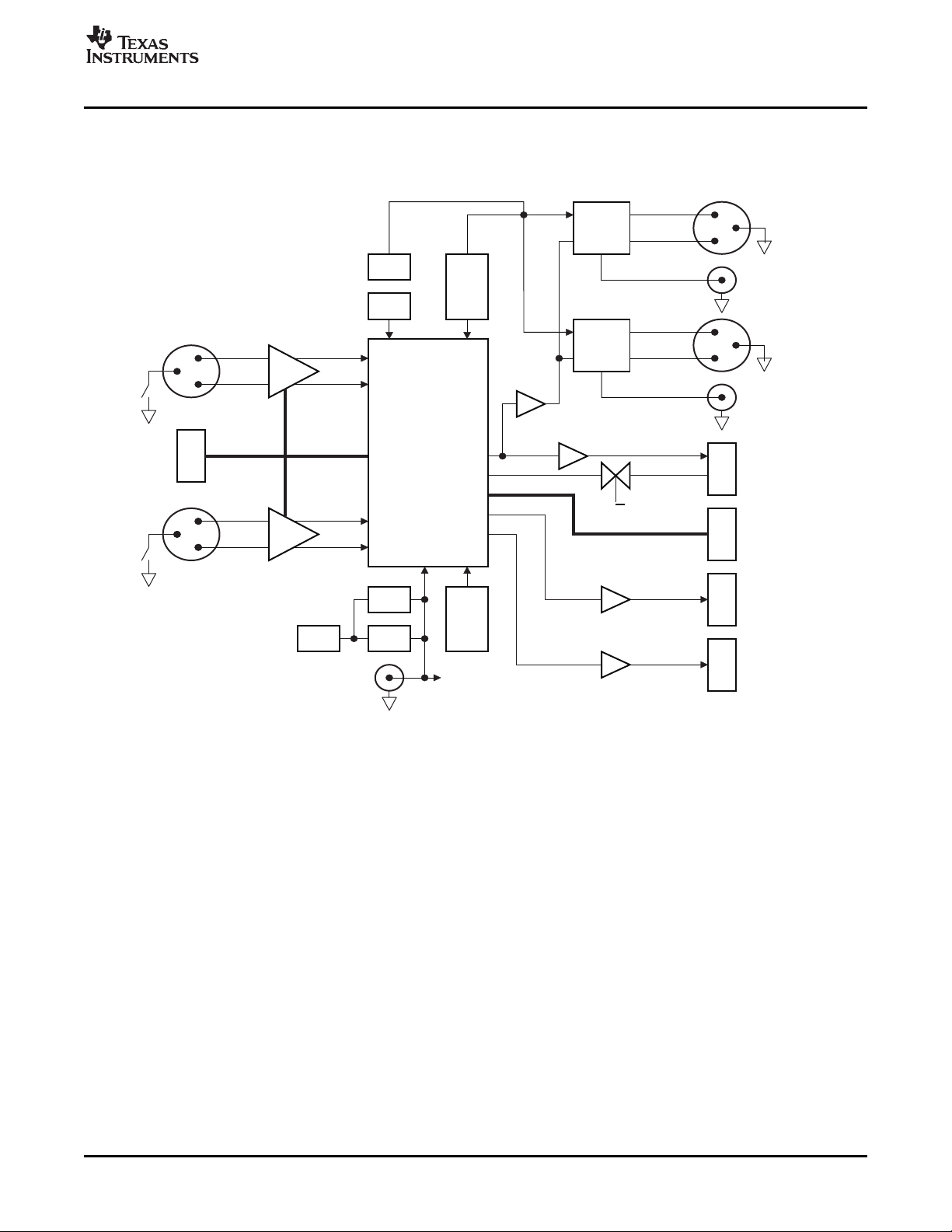
Figure 2 shows a simplified block diagram for the PCM4222EVM circuit functions. The blocks labeled FDA
are the OPA1632 fully differential amplifier input circuits (U4 and U5). The blocks labeled DIT are the
DIT4192 digital audio interface transmitters (U13 and U14). Two transmitters are required to support AES3
Single-Channel, Double Sampling Frequency applications.
Introduction
Figure 2. Simplified Block Diagram for the PCM4222EVM Evaluation Module
SBAU124 – December 2006 PCM4222EVM User's Guide 5
Submit Documentation Feedback
Page 6
www.ti.com
Hardware Configuration
2 Hardware Configuration
This section provides information on the PCM4222EVM hardware configuration, including power supplies
and switch settings. Evaluation module handling information and absolute operating conditions are also
provided.
2.1 Electrostatic Discharge Warning
Failure to observe proper ESD handling procedures may result in damage to
PCM4222EVM components.
Many of the components used in the assembly of the evaluation module are susceptible to damage by
electrostatic discharge (ESD). Customers are advised to observe proper ESD handling procedure when
unpacking and handling the EVM. All handling should be performed at an approved ESD workstation or
test bench while wearing an appropriate grounding device. Failure to observe ESD handling procedures
may result in damage to EVM components.
2.2 Absolute Operating Conditions
Exceeding the absolute operating conditions may result in improper operation
or damage to the evaluation module and/or the equipment connected to it.
CAUTION
CAUTION
Table 1 summarizes the critical data points for the PCM4222EVM absolute operating conditions.
Table 1. Absolute Operating Conditions
PARAMETER MIN MAX UNIT
Analog Power Supplies
+15V -0.3 +16.0 VDC
-15V +0.3 -16.0 VDC
EXT VCC -0.3 +6.0 VDC
Digital Power Supplies
+5V -0.3 +5.5 VDC
EXT VDD -0.3 +4.0 VDC
Analog Input Voltage (Measured Differentially at J1 or J2)
Left Channel Analog Input (J1) 4 x VCC V
Right Channel Analog Input (J2) 4 x VCC V
Digital Input Voltage
Audio Serial Port (J6) -0.3 +4.0 V
EXT CLOCK (J11) -0.3 +6.5 V
Digital Output Voltage
Connectors J4, J5, and J6 -0.3 VDD + 0.3
Connector J7, J9 (terminated with 110 ohms) 4.5 V
Connector J8, J10 (terminated with 75 ohms) 3.6 V
Temperature
Ambient Operating Range 0 +70 ° C
PP (DIFF)
PP (DIFF)
PP (DIFF)
PP
PCM4222EVM User's Guide6 SBAU124 – December 2006
Submit Documentation Feedback
Page 7

www.ti.com
2.3 Power Supplies
VCC +5V +3.3V VDD
+5V DGND
+15V
+15V
-15V
-15V
AGND
EXT
VCC
EXT
VDD
+3.3V
Regulator
+4.0V
Regulator
J12
DigitalPower
J3
AnalogPower
REG
1
3
2
4
EXT
JMP6
REG
1
3
2
4
EXT
JMP5
U23 U22
Hardware Configuration
The PCM4222EVM includes two terminal blocks for connection of external power supplies. Terminal block
J3 supports analog power supplies, while terminal block J12 supports digital power supplies. Refer to
Table 1 for absolute operating conditions. Table 2 shows the recommended power supply range for the
PCM4222EVM.
Table 2. Recommended Power Supply Range
PARAMETER MIN MAX UNIT
Analog Power Supplies (J3)
+15V +6.0 +15.0 VDC
-15V -6.0 -15 VDC
EXT VCC +3.8 +4.2 VDC
Digital Power Supplies (J12)
+5V +4.5 +5.5 VDC
EXT VDD +2.4 +3.6 VDC
The PCM4222EVM requires a minimum of two external dc power supplies for the analog functions. The
two power supplies are labeled as +15V and –15V on terminal block J3. The +15V and –15V supplies
should be regulated and capable of providing a minimum of 200mA of current each.
The PCM4222 requires a +4.0V nominal dc supply for operation of the internal analog circuitry.
Designated as VCC, this supply may be derived from the +15V analog power supply using an onboard
linear regulator circuit, comprised of U23 and the associated components. The regulator circuit is
protected in the event that a short-circuit occurs between the +15V supply and ground. The EVM also
supports an external +4.0V power supply, which may be connected at the EXT VCC terminal of J3.
Jumper JMP6 is used to select the onboard regulated supply or an external power source. Figure 3
illustrates the jumper options.
Figure 3. Power Supply Jumper Configuration
In addition to the analog supplies, the PCM4222EVM requires at least one digital power supply, connected
at the +5V terminal of J12. This supply is nominally +5V dc, and should be provided by a regulated
voltage source capable of sourcing a minimum of 200mA. The +3.3V required for the PCM4222 digital
section and external support logic may be derived from the +5V supply using an onboard linear voltage
regulator (U22). Alternatively, an external regulated VDD supply may be connected via the EXT VDD
terminal of J12. Refer to Figure 3 for the configuration of jumper JMP5, which is used to select the source
of the VDD power supply.
SBAU124 – December 2006 PCM4222EVM User's Guide 7
Submit Documentation Feedback
Page 8

www.ti.com
Hardware Configuration
2.4 Analog Inputs
The left and right channel analog input sources for the PCM4222 are provided through connectors J1 and
J2, respectively. The J1 and J2 connectors accommodate both 3-pin balanced XLR and 1/4-inch balanced
TRS input connections. Pin 1 for both connector J1 and J2 include a ground lift jumper.
Each analog input is buffered by an input circuit employing the OPA1632 fully differential audio amplifier,
selected for its low noise and distortion, and fully-differential input-to-output architecture. The buffer circuit
provides attenuation (nominal gain = 0.482, or –6.34dB) and low-pass antialiasing filter functions. The
printed circuit board (PCB) layout supports limited board stuff options for experimentation. The full-scale
input voltage for the input buffer circuit is approximately 4.2V
(or +14.6845dBu) differential, given a
RMS
nominal VCC supply of +4.0V for the PCM4222 and a source impedance of 40 Ω . Due to the full-scale
input voltage varying slightly from one PCM4222 device to another, the full-scale input swing should be
calibrated for each EVM individually, adjusting the input voltage level until a 0dBFS output level is
indicated.
The common-mode bias for each OPA1632 is provided by the corresponding VCOML or VCOMR outputs
from the PCM4222. The VCOML and VCOMR outputs are buffered by OPA227 low-noise precision op
amps, configured as voltage followers. A buffer is required because of the low input impedance of the
OPA1632 V
pin.
OCM
8 PCM4222EVM User's Guide SBAU124 – December 2006
Submit Documentation Feedback
Page 9

www.ti.com
2.5 Master Clock Source
The PCM4222 and the DIT4192 transmitters require a master clock source for operation. The master
clock can be generated using one of two crystal oscillators (designated as X1 or X2), or from an external
clock source connected at the BNC input connector J11. The clock generated by the crystal oscillators or
external source is used directly by the DIT4192 transmitters. However, this clock must be divided by two
when used by the PCM4222. A D-type flip-flop (U21) performs this function.
Oscillator X1 is fixed at 22.5792MHz, and may provide the master clock for 44.1kHz and related sampling
rates, including 88.2kHz and 176.4kHz. Oscillator X2 is fixed at 24.576MHz, and may provide the master
clock for 48kHz and related sampling rates, including 96kHz and 192kHz.
An external clock source (EXT CLOCK), may be input at BNC connector J11 and is buffered by U19. The
buffer includes a tri-state output, so that it may be disabled when one of the crystal oscillators is used as
the master clock source. Buffer U19 is always operated from the +3.3V supply generated by voltage
regulator U22, and is tolerant to +5V input logic levels. The maximum external master clock frequency is
27.648MHz.
Table 3 summarizes the master clock source selection using switch SW6. Note that the user should not
enable oscillators X1 and X2 simultaneously, because it will result in output contention and improper
operation. Table 4 lists the master clock rate requirements for commonly used digital audio sampling
rates.
Switch SW6,
EXTCLK Switch SW6, X2 Switch SW6, X1 Master Clock Selection
Hardware Configuration
Table 3. Master Clock Source Selection
LO LO LO External Clock connected at BNC input J11
HI LO HI Oscillator X1, 22.5792MHz ± 50ppm
HI HI LO Oscillator X2, 24.576MHz ± 50ppm
HI HI HI Not allowed due to oscillator output contention
Table 4. Master Clock Frequencies for Common Output Sampling and Data Rates
PCM4222 Output Mode Output Rate (MHz) (MHz)
8kHz 4.096 2.048
PCM Normal
PCM Double Speed
PCM Quad Speed
DSD, 64x Oversampling 2.8224MHz 22.5792 11.2896
DSD, 128x Oversampling 5.6448MHz 22.5792 11.2896
Multi-Bit Modulator 6.144MHz 24.576 12.288
32kHz 16.384 8.192
44.1kHz 22.5792 11.2896
48kHz 24.576 12.288
88.2kHz 22.5792 11.2896
96kHz 24.576 12.288
176.4kHz 22.5792 11.2896
192kHz 24.576 12.288
EVM Master Clock Rate PCM4222 MCKI Clock Rate
SBAU124 – December 2006 PCM4222EVM User's Guide 9
Submit Documentation Feedback
Page 10

www.ti.com
Hardware Configuration
2.6 Manual Reset Operation
The PCM4222EVM includes two momentary-contact, normally open, push-button switches that are used
for manual reset functions. Switch SW4 can be used to reset the PCM4222, while switch SW5 can be
used to reset the DIT4192 transmitters. In each case, simply press and then release the corresponding
push-button switch to force an external reset for these devices.
2.7 PCM Output Mode Configuration
The PCM4222 outputs linear encoded PCM data at the audio serial port output, header J6, or via the
DIT4192 AES3 transmitters. The PCM data is binary two’s complement, with the most significant bit of the
data transmitted first. The audio data word length may be 24, 20, 18, or 16 bits. Several audio formats are
supported. See section Section 2.7.2 (Audio Serial Port ) of this document and the PCM4222 datasheet for
details.
The PCMEN input (pin 16) is used to enable and disable the PCM output mode. Table 5 summarizes the
operation of the PCMEN element on switch SW1. When the PCM output is disabled, the DATA (pin 32)
output is forced low. If the PCM4222 is set to Master mode, the BCK (pin 33) and LRCK (pin 34) clock
outputs are also forced low when the PCM output is disabled.
Table 5. PCM Output Mode Configuration
Switch SW1, PCMEN PCM Output Mode
LO PCM Output Disabled
HI PCM Output Enabled
2.7.1 Sampling Mode
The PCM output operates in one three sampling modes: Normal, Double Speed, or Quad Speed. Normal
mode supports 128x oversampling with output sampling rates up to 54kHz. Double Speed mode supports
64x oversampling with output sampling rates from 54kHz to 108kHz. Quad Speed mode supports 32x
oversampling with output sampling rates from 108kHz to 216kHz.
The sampling mode is determined by the state of the FS0 and FS1 inputs (pins 19 and 20, respectively).
FS0 and FS1 are configured using the like named elements of switch SW1. Table 6 summarizes the
available settings for FS0 and FS1.
Table 6. PCM Sampling Mode Selection
Switch SW1, FS1 Switch SW1, FS0 PCM Sampling Mode
LO LO Normal
LO HI Double Speed
HI LO Quad Speed
HI HI Reserved
PCM4222EVM User's Guide10 SBAU124 – December 2006
Submit Documentation Feedback
Page 11

www.ti.com
2.7.2 Audio Serial Port
For PCM mode, the audio data may be output via the audio serial port, which is buffered and routed to
header J6. The audio serial port header pin configuration is shown in Table 7 . The BCK and LRCK clocks
may be outputs or inputs, depending upon the Master or Slave mode configuration of the port
Header J6 Pin Number Audio Serial Port Signal Name, Description
In Master mode, the BCK and LRCK clocks are output pins, and are derived from the PCM4222 MCKI
clock input (pin 35). The BCK clock rate depends on the audio data format selection. The LRCK clock rate
is always equal to the output sampling rate. In Slave mode, the BCK and LRCK clocks are input pins,
sourced from an external audio serial port master, such as a digital signal processor serial port, a serial
timing generator, or a programmable logic device. Once again, the LRCK clock rate is always equal to the
desired output sampling rate. The BCK clock rate depends on the audio data format selected. Refer to the
PCM4222 datasheet for audio serial port operational details.
The Slave/Master mode operation is determined by the state of the S/ M input (pin 39), which is controlled
via the S/ M element on switch SW3. Table 8 summarizes the operation of the S/ M switch.
Hardware Configuration
Table 7. Audio Serial Port Header Configuration
1 SCKO, System Clock Output (same as PCM4222 MCKI clock)
3 BCK, Audio Data Bit Clock Input or Output
5 LRCK, Audio Left/Right Word Clock Input or Output
7 DATA, PCM Audio Data Output
2,4,6,8,9,10 Ground
Table 8. Audio Serial Port Slave/Master Mode Selection
Switch SW3, S/ M Slave or Master Mode
LO Master
HI Slave
The audio data format is selected using the FMT0 and FMT1 inputs (pins 44 and 43, respectively), which
are controlled by the FMT0 and FMT1 elements on switch SW3. Table 9 summarizes the operation for the
FMT0 and FMT1 switches.
Table 9. Audio Serial Port Data Format Selection
Switch SW3, FMT1 Switch SW3, FMT0 Audio Data Format
LO LO Left Justified
LO HI I2S
HI LO TDM
HI HI TDM with One BCK Period Delay
SBAU124 – December 2006 PCM4222EVM User's Guide 11
Submit Documentation Feedback
Page 12

www.ti.com
Hardware Configuration
When selecting a TDM data format, it is necessary to select a sub-frame assignment for the PCM4222 so
that the device is set to transmit data during the appropriate time slots in the TDM frame. When the
PCM4222 is not transmitting, the DATA output (pin 32) is forced to a high impedance state so that another
PCM4222 device may transmit on the TDM data bus. The sub-frame assignment is selected using the
SUB0 and SUB1 inputs (pins 26 and 25, respectively). These inputs are controlled using the SUB0 and
SUB1 elements on switch SW2. Table 10 summarizes the operation for the SUB0 and SUB1 switches.
Table 10. TDM Sub-frame Assignment
Switch SW2, SUB1 Switch SW2, SUB0 Sub-Frame Assignment
LO LO Sub-Frame 0
LO HI Sub-Frame 1
HI LO Sub-Frame 2
HI HI Sub-Frame 3
Typically, the PCM4222 will be configured to output 24-bit PCM data. However, the PCM4222 supports
data word length reduction using Triangular PDF dithering. This architecture allows the device to output
20, 18, or 16 bits of audio data when needed. The output word length is determined by the OWL0 and
OWL1 inputs (pins 42 and 41, respectively). These pins are controlled by the OWL0 and OWL1 element
switch SW3. Table 11 summarizes the operation of the OWL0 and OWL1 switches.
Table 11. PCM Output Word Length Selection
Switch SW3, OWL1 Switch SW3, OWL0 Output Data Word Length
LO LO 24 bits
LO HI 18 bits
HI LO 20 bits
HI HI 16 bits
2.7.3 Digital Decimation Filter
The PCM4222 includes a linear phase digital decimation filter that is used to downsample the delta-sigma
modulator output and provide low-pass antialiasing filtering. The decimation filter includes two selectable
frequency responses: Classic and Low Group Delay. Refer to the PCM4222 datasheet for plots and
specifications related to each filter response. The DF input (pin 21) is used to select the desired frequency
response. This input is controlled using the DF element on switch SW1. Table 12 summarizes the
operation of the DF switch.
Table 12. Digital Decimation Filter Configuration
Switch SW1, DF Digital Decimation Filter Response
LO Classic
HI Low Group Delay
PCM4222EVM User's Guide12 SBAU124 – December 2006
Submit Documentation Feedback
Page 13

www.ti.com
2.7.4 Digital High-Pass Filter
The PCM4222 includes digital high-pass filtering that removes the dc component from the output signal.
The right and left channel filters can be enabled and disabled individually, using the HPFDR (pin 17) and
HPFDL (pin 18) inputs, respectively. These inputs are controlled via the HPFDR and HPFDL elements on
switch SW1. Table 13 summarizes the operation for these switches.
Switch SW1, HPFDR or HPFDL Digital High-Pass Filter Function
2.7.5 Overflow Output Indicators
The PCM4222 includes two active-high overflow indicators, one each for the left and right channels. The
overflow indicators are provided at the OVFL (pin 37) and OVFR (pin 38) outputs. These outputs are
buffered by U17 and U18. The buffers drive light emitting diodes LED1 and LED2 on the EVM, providing
visual overflow indication for the left and right channels, respectively.
2.7.6 AES3 Transmitter Operation
The EVM includes two Texas Instruments DIT4192 digital audio interface transmitters, U13 and U14. The
transmitters accept either Left Justified or I2S formatted PCM output data from the PCM4222 and then
encode it into an AES3 data stream, which is output at connectors J7 through J10. A tri-state buffer (U11)
is used to enable/disable the clock and data flow from the PCM4222 to the DIT4192 devices. The DIT
switch on SW3 is used to enable or disable the buffer. Table 14 summarizes the DIT switch settings.
Hardware Configuration
Table 13. Digital High-Pass Filter Switch Operation
LO Enabled
HI Disabled
Table 14. DIT4192 Serial Data and Clock Enable Operation
Switch SW3, DIT DIT4192 Input Data/Clock Enable
LO Enabled. Data and clocks flow from the PCM4222 to U13 and U14.
HI
Disabled. The tri-state buffer outputs are high impedance, with no
clocks or data supplied to U13 and U14.
The DIT4192 includes an on-chip master clock divider, which is used to generate the output frame rate
clock for the AES3-encoded data. For PCM data, the output frame rate is normally the same as the
PCM4222 output sampling rate. The exception is for Single-Channel, Double Sampling Frequency
transmission, when the DIT4192 Mono mode operation is invoked (this topic is discussed later in this
section).
The DITCLK0 and DITCLK1 elements on switch SW3 determine the master clock divider settings for the
transmitters. Table 15 summarizes the operation for the DITCLK0 and DITCLK1 switches, and indicates
the selections corresponding to the three sampling modes for the PCM4222.
Table 15. DIT4192 Master Clock Divider Configuration
Switch SW3, DITCLK1 Switch SW3, DITCLK0 DIT4192 Master Clock Divider
LO LO Divide by 128 (PCM4222 Quad Speed mode)
LO HI Divide by 256 (PCM4222 Dual Speed mode)
HI LO Divide by 384 (Not Used)
HI HI Divide by 512 (PCM4222 Normal mode)
SBAU124 – December 2006 PCM4222EVM User's Guide 13
Submit Documentation Feedback
Page 14

www.ti.com
Hardware Configuration
The DIT4192 input serial port supports Left Justified and I2S formatted PCM data from the PCM4222
audio serial port. The TDM data formats are not supported by the DIT4192 input serial port. The DITFMT
element on switch SW3 is used to select the proper data format for the DIT4192, and must match the data
format that is selected using the FMT0 and FMT1 elements on switch SW3. Table 16 summarizes the
operation for and relationship between the DIT4192 and PCM4222 data format switches.
Table 16. DIT4192 Data Format Selection
Switch SW3, FMT1 Switch SW3, FMT0 Switch SW3, DITFMT Audio Data Format
LO LO LO Left Justified
LO HI HI I2S
HI X X TDM formats are not supported
Although one DIT4192 transmitter supports transmission of two-channels of PCM audio data at
sampling/frame rates up to and including 216kHz, it is sometimes desirable to use two DIT4192 devices,
each carrying data for only a single channel (left or right, respectively) at a frame rate equal to one-half the
PCM4222 output sampling rate. This is referred to as Single-Channel, Double Sampling Frequency
transmission in the AES3-2003 standard. The DIT4192 Mono mode is used to implement this form of
transmission.
Mono mode is enabled or disabled using the MONO input (pin 21) of the DIT4192 transmitters. The
DITMONO element on switch SW3 is used to control the MONO pin. Table 17 demonstrates the operation
of the DITMONO switch.
Table 17. DIT4192 Transmission Mode Configuration
Switch SW3, DITMONO DIT4192 Transmission Mode
LO Two-channel
HI Single-Channel Double Sampling Frequency
The MDAT input (pin 20) of the DIT4192 transmitters is used to select left or right channel for transmission
in Mono mode. The MDAT pin of transmitter U13 is connected to ground, selecting the left input channel.
The MDAT pin of transmitter U14 is connected to VDD, selecting the right input channel. In Mono mode,
the left channel is transmitted from AES3 Output #1 (connectors J7 and J8), while the right channel is
transmitted on AES3 Output #2 (connectors J9 and J10).
When Mono mode is disabled, both the left and right channels are output on both AES3 Output #1 and #2.
This allows for simultaneous balanced and unbalanced transmission of the AES3-encoded output data.
Mono Mode Example: Assume that you are transmitting 192kHz two-channel data using the AES3
transmitters, with a 24.576MHz master clock and the clock dividers set to divide by 128. By simply
enabling Mono mode (setting the DITMONO switch to HI), the transmission converts to Single-Channel,
Double Sampling Frequency mode with an output frame rate equal to 96kHz. There is no need to change
the master clock divider or frequency, because the DIT4192 manages the change in output frame rate
automatically.
PCM4222EVM User's Guide14 SBAU124 – December 2006
Submit Documentation Feedback
Page 15

www.ti.com
2.8 DSD Output Mode Configuration
The PCM4222 supports a one-bit Direct Stream Digital (DSD) data output, which operates at either 64x or
128x the base PCM output sampling rate. The PCM4222 allows both the DSD and PCM output modes to
be enabled simultaneously. The DSD data for the left and right channels and the associated bit clock are
output at the DSD data port, or header J5. Table 18 lists the pin configuration for header J5.
The DSD output mode is enabled or disabled using the DSDEN input (pin 22). This input is controlled via
the DSDEN element on switch SW1. Table 19 summarizes the operation of this switch. When the DSD
output is disabled, DSDCLK (pin 27), DSDL (pin 28), and DSDR (pin 29) are forced low.
Hardware Configuration
Table 18. DSD Data Port Header Pin Configuration
Header J5 Pin Number DSD Data Port Signal Name, Description
1 DSDCLK, DSD Bit Clock Output
3 DSDL, One-bit DSD Data Output for the Left Channel
5 DSDR, One-bit DSD Data Output for the Right Channel
2,4,6,7,8,9,10 Ground
Table 19. DSD Output Mode Configuration
Switch SW1, DSDEN DSD Output Mode
LO Disabled
HI Enabled
The DSD output data rate may be set to 64x or 128x the base PCM rate (typically 44.1kHz). The output
rate is selected via the DSDMODE input (pin 24). This input is controlled via the DSDMODE element on
switch SW1. Table 20 summarizes the operation of this switch.
Table 20. DSD Output Rate Selection
Switch SW1, DSDMODE DSD Output Data Rate
LO 64x Oversampled Data with Output Rate = MCKI ÷ 4
HI 128x Oversampled Data with Output Rate = MCKI ÷ 2
For more information regarding DSD output mode operation, timing, and specifications, see the PCM4222
datasheet .
SBAU124 – December 2006 PCM4222EVM User's Guide 15
Submit Documentation Feedback
Page 16

www.ti.com
Hardware Reference
2.9 Modulator Output Operations
The PCM4222 supports a multi-bit modulator (MBM) output mode, where the 6-bit data for the left and
right channels are output directly from the delta-sigma modulators. The MBM output data are buffered and
routed to the modulator data port, or header J4. Table 21 lists the pin configuration for header J4.
The MBM output mode is enabled or disabled using the MODEN input (pin 23). This input is controlled via
the MODEN element on switch SW1. Table 22 summarizes the operation of this switch. When MBM mode
is enabled, the PCM and DSD output modes are disabled, because some of the pins used for these
modes are remapped as modulator data and clock outputs. The PCMEN input (pin 16) must be set to the
LO position when the MBM output is enabled. When MBM mode is disabled, all data and clock outputs
associated with the interface are driven low (assumes PCM and DSD modes are also disabled).
Table 21. Modulator Data Port Header Pin Configuration
Header J4 Pin Name Modulator Data Port Signal Name, Description
1 MOD1, Modulator Data Output 1 (LSB)
3 MOD2, Modulator Data Output 2
5 MOD3, Modulator Data Output 3
7 MOD4, Modulator Data Output 4
9 MOD5, Modulator Data Output 5
11 MOD6, Modulator Data Output 6 (MSB)
13 MCKO, Modulator Data Clock Output (Rate = MCKI)
15 WCKO, Modulator Word Clock Output (Rate = MCKI ÷ 2)
2,4,6,8,10,12,14,16,17,18,19,20 Ground
3 Hardware Reference
Table 22. Multi-Bit Modulator (MBM) Output Mode Configuration
Switch SW1, MODEN Switch SW1, PCMEN Switch SW1, DSDEN MBM Output Mode
LO X X Disabled
HI LO X Enabled
Referring to the electrical schematic in Figure 4 , when MODEN is set to a LO state, the outputs of tri-state
buffer U6 are enabled, allowing the elements of switch SW1 and SW2 that are related to the PCM and
DSD output modes to control the configuration of the PCM4222. When MODEN is HI, the outputs of buffer
U6 are disabled and set to a high-impedance state. In addition, when MODEN is HI, tri-state buffer U7 is
enabled, allowing the modulator output data and clocks to be routed to the modulator data port (header
J4).
For more information regarding Multi-Bit Modulator output mode operation, timing, and specifications, see
the PCM4222 datasheet .
This section provides the electrical schematics and the Bill of Materials for the PCM4222EVM evaluation
board. The components shown in the schematic are listed in Table 23 , the Bill of Materials, for reference.
16 PCM4222EVM User's Guide SBAU124 – December 2006
Submit Documentation Feedback
Page 17
www.ti.com
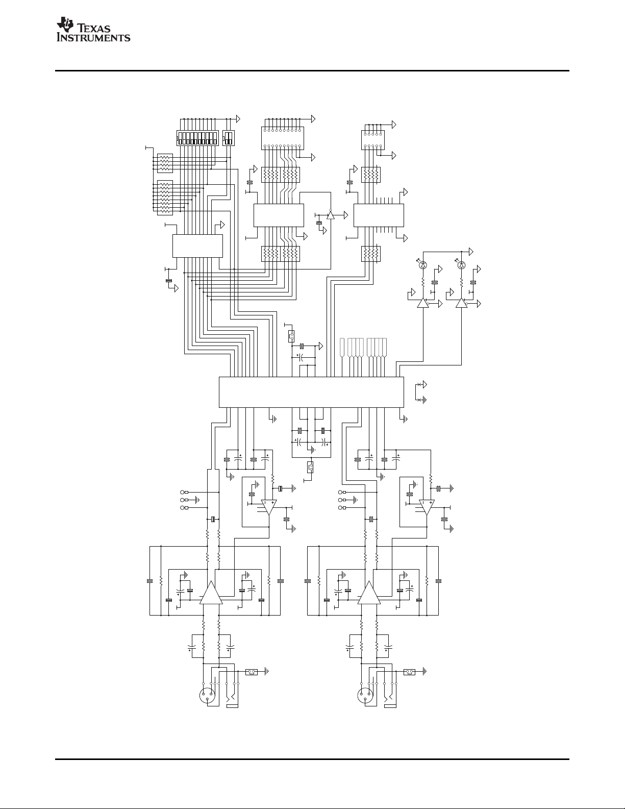
3.1 Electrical Schematics
RTS
231
G
J2
RIGHTCH. ANALOGIN
RTS
231
G
J1
LEFTCH. ANALOG IN
R5
0
R11
560
R6
0
R12
560
R18
270
C21 0.1uF
R17
270
C7
1nF
LED1
C54
NI
LED2
821
36
4
5
VOCM
7
+
_
+
_
EN
U4
OPA1632DGN
R22
40.2
R21
40.2
1
2
JMP1
R70R8
0
C62
2.7nF
A12A23A34A45A56A67A78A8
9
B118B217B316B415B514B613B712B8
11
GND
10
DIR
1
VCC
20
OE
19
U7
SN74ALVC245PW
A12A23A34A45A56A67A78A8
9
B118B217B316B415B514B613B712B8
11
GND
10
DIR
1
VCC
20
OE
19
U6
SN74ALVC245PW
C8
1nF
RN1
10K
C55
NI
12021931841751661571481391210
11
SW1
1 2
JMP3
C51
22uF
R15
270
RN2
10K
-15V
R16
270
TP2
VINL-
TP3
VINL+
2
3
6
7
4 1
8
U2
OPA227UA
C31
0.1uF
C30
0.1uF
-15V
+15V
C3
NI
C4
NI
C32
0.1uF
R24
1k
142
3
SW2
VDD
C12
0.1uF
VDD
246
135
78910111213141516171819
20
J4
MODULATOROUTPUTPORT
RN3 100
RN4 100
RN5 100
RN6 100
C20
0.1uF
VDD
2
4
53
U8
SN74LVC1G04DBV
C28
0.1uF
VDD
246
135
789
10
J5
DSDDATAPORT
A12A23A34A45A56A67A78A8
9
B118B217B316B415B514B613B712B8
11
GND
10
DIR
1
VCC
20
OE
19
U15
SN74ALVC245PW
VDD
C29
0.1uF
RN14
100
RN15
100
VDD
C19
0.1uF
C25
0.1uF
C24
0.1uF
+15V
C50
22uF
C22
0.1uF
R1
0
R9
560
R2
0
R10
560
C10
0.1uF
C5
1nF
C52
NI
821
36
4
5
VOCM
7
+
_
+
_EN
U5
OPA1632DGN
R20
40.2
R19
40.2
R30R4
0
C61
2.7nF
C6
1nF
C53
NI
1 2
JMP4
C49
22uF
R13
270
-15V
R14
270
TP5
VINR-
TP6
VINR+
2
3
6
7
4 1
8
U3
OPA227UA
C14
0.1uF
C13
0.1uF
-15V
+15V
C1
NI
C2
NI
C15
0.1uF
R23
1K
C26
0.1uF
C18
0.1uF
C17
0.1uF
C16
0.1uF
+15V
C48
22uF
C9
0.1uF
1
2
JMP2
VCC
FMT1
FMT0
S/M
VDD
OWL1
OWL0
LRCK
SCKI
DATA
BCK
/RST
2
4
1
5 3
U17
SN74LVC1G125DBV
2
4
1
5 3
U18
SN74LVC1G125DBV
VDD
C27
0.1uF
VDD
C33
0.1uF
VDD
VDD
C63
100
C64
NI
C68
NI
C67
100
C65
100
C69
100
C66
100
HPFDL
18
FS019FS1
20
LRCK
34
SUB1
25
DSDMODE
24
SUB0
26
DSDL
28
DSDCLK
27
HPFDR
17
VINL-10VINL+
11
AGND
12
REFGNDL14VCOML
13
VDD
31
DATA
32
VREFL
15
DSDR
29
DGND
30
AGND8VCC2
9
DGND
40
MODEN
23
DSDEN
22
OWL1
41
VCOMR
48
FMT0
44
AGND
6
FMT1
43
VCC1
4
VINR+
3
AGND
5
REFGNDR47AGND
1
VINR-
2
SCKI35/RST
36
OVFL
37
OVFR
38
S/M
39
DGND
45
FMODE
21
VREFR
46
BGND
7
PCMEN
16
BCK
33
OWL0
42
U1
PCM4222PFB
TP1
AGND
TP4
AGND
Hardware Reference
The electrical schematics for the PCM4222EVM are shown in Figure 4 and Figure 5 .
SBAU124 – December 2006 PCM4222EVM User's Guide 17
Submit Documentation Feedback
Figure 4. PCM4222EVM Schematics, Page 1 of 2
Page 18

www.ti.com
C37
0.1uF
VDD
SW5
/DITRST
SW4
/ADCRST
C72
0.01uF
R28
10K
C71
0.01uF
R27
10K
/RST
RN12
10K
1202193184175166157148139
121011
SW3
FMT1
OWL0
FMT0
OWL1
S/M
DITCLK1
DITCLK0
/DIT
DITFMT
RN13
10K
VDD
EN
1
OUT
3
VCC4GND
2
X1
SM7745HSV-22.5792M
EN
1
OUT
3
VCC4GND
2
X2
SM7745HSV-24.576M
C70
0.01uF
C73
0.01uF
+3.3V
+3.3V
2
4
1
53
U19
SN74LVC1G125DBV
J11
EXTCLOCK
R25
75
C34
0.1uF
2
4
1
53
U20
SN74L
V
C1G125DBV
C36
0.1uF
1CLR
1
1D
2
1CLK
3
1PRE
4
1Q51Q
6
GND
7
2Q82Q92PRE102CLK112D122CLR13VDD
14
U21
SN74LVC74APW
VDD
A12A23A34A45A56A67A78A8
9
B118B217B316B415B514B613B712B8
11
GND
10
DIR
1
VCC
20
OE
19
U9
SN74ALVC245PW
A12A23A34A45A56A67A78A8
9
B118B217B316B415B514B613B712B8
11
GND
10
DIR
1
VCC
20
OE
19
U11
SN74ALVC245PW
VDD
RN7
100
RN8
100
RN9
100
RN10
100
246
135
789
10
J6
AUDIOSERIAL PORT
2
4
1
53
U10
SN74L
V
C1G125DBV
C41
0.1uF
C42
0.1uF
S/M
VDD
VDD
C43
0.1uF
VDD
/DIT
CSS1COPY/C2L3CLK14CLK05MCLK6VIO7DGND8FMT09FMT110SCLK11SYNC12SDATA13M/S
14
MODE
28
U
27V26
BLS
25
BLSM
24
EMPH
23
AUDIO
22
MONO
21
MDAT
20
VDD
19
TX+
18
TX-
17
DGND
16
RST
15
U13
DIT4192IPW
CSS1COPY/C2L3CLK14CLK05MCLK6VIO7DGND8FMT09FMT110SCLK11SYNC12SDATA13M/S
14
MODE
28
U
27V26
BLS
25
BLSM
24
EMPH
23
AUDIO
22
MONO
21
MDAT
20
VDD
19
TX+
18
TX-
17
DGND
16
RST
15
U14
DIT4192IPW
VDD
C79
10uF
C80
10uF
C38
0.1uF
C39
0.1uF
C46
0.1uF
C82
10uF
+5V
+5V
C40
0.1uF
R29
110
C47
0.1uF
R30
110
REG
J8
AES3
O
UTPUT
#
1
7
5
o
hms
J10
AES3OUTPUT#2 75 ohms
LRCK
BCK
SCKI
DATA
C45
0.1uF
VDD
C81
10uF
+3.3V
C35
0.1uF
VDD
C56
NI
R26
75
C75
0.01uF
C76
0.01uF
C74
0.01uF
C78
0.01uF
C77
0.01uF
C89
100uF
C88
100uF
C85
100uF
C86
100uF
C87
100uF
+15V
+5V
+3.3V
C83
10uF
C84
10uF
123
4
JMP5
EXT
EXTVCC
-15V
1
2
3
4
J12
DIGITALPOWER
1
2
3
4
J3
ANALOGPOWER
TP7
+5V
VDD
DIT_SYNC
DIT_SCLK
DIT_SDATA
DIT_MCLK
EXTVDD
1A11Y22A32Y43A53Y6GND
7
4Y
84A95Y105A11
6Y
12
6A
13
VCC
14
U16
SN74AHC14PW
1827364
5
SW6
DIPSWITCH-4
RN16
10K
+3.3V
1
4
5
687
PRI
SEC1
SEC2
T2
SC939-06
1
4
5
687
PRI
SEC1
SEC2
T1
SC939-06
VIN
3
VOUT
2
GND
1
VOUT
4
U22
REG1117-3.3
C90
100pF
C91
100pF
2
3
1
G
J7
AES3OUTPUT #1110ohm
s
2
3
1
G
J9
AES3OUTPUT #2110ohm
s
REG
123
4
JMP6
EXT
+15V
VCC
R31
240
R32
200
R33
324
C94
1uF
C92
NI
C93
10uF
D2
DL4002
D1
DL4002
+4V
2
4
1
53
U24
SN74L
V
C1G125DBV
C95
0.1uF
VDD
VIN
3
VOUT
2
GND
1
VOUT
4
U23
LM317M
Hardware Reference
PCM4222EVM User's Guide18 SBAU124 – December 2006
Figure 5. PCM4222EVM Schematics, Page 2 of 2
Submit Documentation Feedback
Page 19

www.ti.com
3.2 Bill of Materials
Hardware Reference
The Bill of Materials is provided as a cross-reference for the components shown in Figure 4 and Figure 5 .
Table 23. Bill of Materials
ITEM QTY VALUE DESIGNATOR DESCRIPTION VENDOR PART NUMBER
1 NI C1-C4 Optional AC Coupling Capacitor N/A N/A
2 2 100pF C90, C91 TDK C1608C0G1H101
3 NI C57-C60 Item Removed from Design N/A N/A
4 4 1nF C5-C8 or or or
5 2 2.7nF C61, C62 or or or
6 9 0.01 µ F C70-C78 TDK C1608X7R1H103K
7 37 0.1 µ F C24-29, C30-C43, TDK C1608X7R1H104K
8 NI C92 TDK C1608X7R1H104K
9 1 1 µ F C94 TDK C1608X7R1C105K
10 6 10 µ F C79-C84 Kemet T491A106K010AT
11 1 10 µ F C93 Kemet T494B106K016AT
12 NI 22 µ F C48-C51 Kemet T491D226K025AT
13 5 100 µ F Kemet T520B107M006ATE070
14 NI 100 µ F C64, C68 Kemet T520B107M006ATE070
15 NI C11, C23 Item Removed from Design N/A N/A
16 5 100 µ F C85-C89 Panasonic EEV-FK1E101XP
17 2 D1, D2 DL4002-TP
18 2 LED1, LED2 LED, SMT, Red Clear, Size = 1206 Lumex SML-LX1206IC-TR
19 2 J1, J2 Neutrik NCJ6FI-H
20 2 J3, J12 3.5mm PCB Terminal Block, 4 poles Weidmuller 996770
21 1 J4 Terminal Strip, 20-Pin (10x2) Samtec TSW-110-07-T-D
22 2 J5, J6 Terminal Strip, 10-Pin (5x2) Samtec TSW-105-07-T-D
23 2 J7, J9 Neutrik NC3MAH-0
24 2 J8, J10 RCA Phono Jack, Black Shell CUI Stack RCJ-041
25 1 J11 Vertical PCB Mount BNC Connector Tyco/AMP 5414305-1
26 4 Terminal Strip, 2 pin (2x1) Samtec TSW-102-07-T-S
27 2 JMP5, JMP6 Terminal Strip, 4 pin (2x2) Samtec TSW-102-07-T-D
28 8 0 Ω R1-R8 Chip Resistor, 0 Ω Shunt, Size = 0805 Panasonic ERJ-6EY0R00V
29 4 40.2 Ω R19-R22 Panasonic ERJ-14NF40R2U
REFERENCE
Chip Capacitor, C0G Ceramic, 100pF
± 5%, 50WV, Size = 0603
Chip Capacitor, PPS Film, 1nF ± 2%,
50WV, Size = 0805
Chip Capacitor, C0G Ceramic, 1nF
± 5%, 50WV, Size = 0805
Chip Capacitor, PPS Film, 2.7nF ± 2%,
50WV, Size = 0805
Chip Capacitor, C0G Ceramic, 2.7nF
± 5%, 50WV, Size = 0805
Chip Capacitor, X7R Ceramic, 0.01 µ F
± 10%, 50WV, Size = 0603
C9, C10, C12-22,
C45-C47, C95
C63, C65-C67, Chip Capacitor, Polymer Tantalum,
C69 100 µ F ± 20%, 6.3WV, Size = B
JMP1, JMP2,
JMP3, JMP4
Chip Capacitor, X7R Ceramic, 0.1 µ F
± 10%, 50WV, Size = 0603
Chip Capacitor, X7R Ceramic, 0.1 µ F
± 10%, 50WV, Size = 0603
Chip Capacitor, X7R Ceramic, 1 µ F
± 10%, 16WV, Size = 0603
Chip Capacitor, Solid Tantalum, 10 µ F
± 10%, 10WV, Size = A
Chip Capacitor, Low ESR Tantalum,
10 µ F ± 10%, 16WV, Size = B
Chip Capacitor, Solid Tantalum, 22 µ F
± 10%, 25WV, Size = D
Chip Capacitor, Polymer Tantalum,
100 µ F ± 20%, 6.3WV, Size = B
Capacitor, Alum Electrolytic, SMT,
100 µ F ± 20%, 25WV
Rectifier, Passivated, 1A, 100V, SMD Micro Commerical
Combo Connector, Female XLR and
TRS, Vertical PC Mount
3-Pin Male XLR Chassis
Connector,Horizontal PC Mount
Chip Resistor, Thick Film, 1%
Tolerance, 40.2 Ω , 1/4W, Size = 1210
Panasonic ECH-U1H102GX5
TDK C2012C0G1H102J
Panasonic ECH-U1H272GX5
TDK C2012C0G272J
MELF Components
SBAU124 – December 2006 PCM4222EVM User's Guide 19
Submit Documentation Feedback
Page 20

www.ti.com
Hardware Reference
Table 23. Bill of Materials (continued)
ITEM QTY VALUE DESIGNATOR DESCRIPTION VENDOR PART NUMBER
30 NI 75 Ω R25 Panasonic ERJ-6ENF75R0V
31 1 75 Ω R26 Panasonic ERJ-6ENF75R0V
32 2 110 Ω R29, R30 Panasonic ERJ-6ENF1100V
33 1 200 Ω R32 or or
34 1 240 Ω R31 or or
35 6 270 Ω R13-R18 Panasonic ERA-6YEB271V
36 1 324 Ω R33 or or
37 4 560 R9-R12 Panasonic ERA-6YEB561V
38 2 1k R23, R24 Panasonic ERJ-6ENF1001V
39 2 10k R27, R28 Panasonic ERJ-6ENF1002V
40 10 100 CTS 742C083101JP
41 5 10k CTS 742C163103JP
42 NI Item Removed from Design N/A N/A
43 2 SW1, SW3 ITT C&K Switch TDA10H0SB1
44 1 SW2 ITT C&K Switch TDA02H0SB1
45 2 SW4, SW5 Omron B3S-1000
46 1 SW6 TDA04H0SB1
47 2 T1, T2 Dual Zo Digital Audio Transformer Scientific Conversion SC939-06LF
48 7 TP1-TP7 Keystone Electronics 5006
49 1 U1 Texas Instruments PCM4222PFB
50 2 U2, U3 Low-Noise Precision Op Amp or or
51 2 U4, U5 Fully-Differential Audio Amplifier Texas Instruments OPA1632DGNG4
52 5 Texas Instruments or
53 1 U8 Single Inverter Texas Instruments SN74LVC1G04DBVRG4
54 6 Single Buffer w/ Tri-State Output Texas Instruments SN74LVC1G125DBVRG4
55 NI U12 Item Removed from Design N/A N/A
56 2 U13, U14 Digital Audio Interface Transmitter Texas Instruments DIT4192IPWRG4
57 1 U16 Hex Schmitt Trigger Inverter Texas Instruments or
58 1 U21 Texas Instruments SN74LVC74APWRG4
REFERENCE
Chip Resistor, Thick Film, 1%
Tolerance, 75 Ω , 1/10W, Size = 0805
Chip Resistor, Thick Film, 1%
Tolerance, 75 Ω , 1/10W, Size = 0805
Chip Resistor, Thick Film, 1%
Tolerance, 110 Ω , 1/10W, Size = 0805
Chip Resistor, Thin Film, 0.1%
Tolerance, 200 Ω , 1/10W, Size = 0805
Chip Resistor, Thin Film, 0.1%
Tolerance, 240 Ω , 1/10W, Size = 0805
Chip Resistor, Metal Film, 0.1%
Tolerance, 270 Ω , 1/10W, Size = 0805
Chip Resistor, Thin Film, 0.1%
Tolerance, 324 Ω , 1/10W, Size = 0805
Chip Resistor, Metal Film, 0.1%
Tolerance, 560 Ω , 1/10W, Size = 0805
Chip Resistor, Thick Film, 1%
Tolerance, 1k Ω , 1/10W, Size = 0805
Chip Resistor, Thick Film, 1%
Tolerance, 10k Ω , 1/10W, Size = 0805
RN3-RN10, RN14, Thick Film Chip Resistor Array 100 Ω ,
RN15 8 Terminal, 4 Resistors
RN1, RN2, RN12, Thick Film Chip Resistor Array 10k Ω ,
RN13, RN16 16 Terminal, 8 Resistors
RN11, RN14,
RN15
DIP Switch, 10 Element, Half Pitch
Surface-Mount, Tape Sealed
DIP Switch, 2 Element, Half Pitch
Surface-Mount, Tape Sealed
Momentary Tact Switch SMT w/o
Ground Terminal
DIP Switch, 4 Element, Half Pitch ITT Cannon
Surface-Mount, Tape Sealed (formerly C&K)
PCB Test Point, Compact,
Through-Hole
High-Performance, 24-Bit/216kHz
Stereo Audio A/D Converter
U6, U7, U9, U11, Octal Bus Transceiver w/ Tri-State
U15 Output
U10, U17-U20,
U24
Dual Positive Edge Triggered D-Type
Flip-Flops with Clear and Preset
Susumu RR1220P-201-B-T5
Digi-Key RR12P200BCT-ND
Susumu RR1220P-241-B-T5
Digi-Key RR12P240BCT-ND
Susumu RR1220P-3240-B-M-T5
Digi-Key RR12P324BCT-ND
Texas Instruments OPA227UAG4
Texas Instruments OPA27GU
SN74ALVC245PWG4
SN74ALVC245PWRG4
SN74AHC14PWG4
SN74AHC14PWRG4
20 PCM4222EVM User's Guide SBAU124 – December 2006
Submit Documentation Feedback
Page 21

www.ti.com
Hardware Reference
Table 23. Bill of Materials (continued)
ITEM QTY VALUE DESIGNATOR DESCRIPTION VENDOR PART NUMBER
59 1 U22 LM1117MP-3.3
60 1 U23 Linear Voltage Regulator, Adjustable LM317MSTT3G
61 1 X1 Oscillator, CMOS Output with Active Pletronics SM7745HSV-22.5792M
62 1 X2 Oscillator, CMOS Output with Active Pletronics SM7745HSV-24.576M
63 6 Shorting Blocks Samtec SNT-100-BK-T-H
64 4 Self-Adhesive Rubber Feet 3M Bumpon SJ-5003
65 1 PWB PCM4222EVM PWB Texas Instruments 6469498
66 NI C52-C56 Stuff Option Capacitors, Size = 0805 N/A N/A
REFERENCE
Texas Instruments
or
Texas Instruments
or
Low Drop-Out Voltage Regulator, National
+3.3V Semiconductor
or
ON Semiconductor
or
Linear Technology
Texas Instruments
or
ON Semiconductor
or
National
Semiconductor
+3.3V, Surface-Mount Clock
High Enable, 22.5792MHz, ± 50ppm
+3.3V, Surface-Mount Clock
High Enable, 24.576MHz, ± 50ppm
TLV1117-33CDCYG3
or
TLV1117-33IDCYG3
or
or
NCP1117ST33T3G
or
LT1117CST-3.3#PBF
LM317MDCYG3
or
or
LM317EMP
SBAU124 – December 2006 PCM4222EVM User's Guide 21
Submit Documentation Feedback
Page 22

FCC Warning
This evaluation board/kit is intended for use for ENGINEERING DEVELOPMENT, DEMONSTRATION, OR EVALUATION
PURPOSES ONLY and is not considered by TI to be a finished end-product fit for general customer use. It generates, uses, and
can radiate radio frequency energy and has not been tested for compliance with the limits of computing devices pursuant to part 15
of FCC rules, which are designed to provide reasonable protection against radio frequency interference. Operation of this
equipment in other environments may cause interference with radio communications, in which case the user at his own expense
will be required to take whatever measures may be required to correct this interference.
EVALUATION BOARD/KIT IMPORTANT NOTICE
Texas Instruments (TI) provides the enclosed product(s) under the following conditions:
This evaluation board/kit is intended for use for ENGINEERING DEVELOPMENT, DEMONSTRATION, OR EVALUATION
PURPOSES ONLY and is not considered by TI to be a finished end-product fit for general consumer use. Persons handling the
product(s) must have electronics training and observe good engineering practice standards. As such, the goods being provided are
not intended to be complete in terms of required design-, marketing-, and/or manufacturing-related protective considerations,
including product safety and environmental measures typically found in end products that incorporate such semiconductor
components or circuit boards. This evaluation board/kit does not fall within the scope of the European Union directives regarding
electromagnetic compatibility, restricted substances (RoHS), recycling (WEEE), FCC, CE or UL, and therefore may not meet the
technical requirements of these directives or other related directives.
Should this evaluation board/kit not meet the specifications indicated in the User’s Guide, the board/kit may be returned within 30
days from the date of delivery for a full refund. THE FOREGOING WARRANTY IS THE EXCLUSIVE WARRANTY MADE BY
SELLER TO BUYER AND IS IN LIEU OF ALL OTHER WARRANTIES, EXPRESSED, IMPLIED, OR STATUTORY, INCLUDING
ANY WARRANTY OF MERCHANTABILITY OR FITNESS FOR ANY PARTICULAR PURPOSE.
The user assumes all responsibility and liability for proper and safe handling of the goods. Further, the user indemnifies TI from all
claims arising from the handling or use of the goods. Due to the open construction of the product, it is the user’s responsibility to
take any and all appropriate precautions with regard to electrostatic discharge.
EXCEPT TO THE EXTENT OF THE INDEMNITY SET FORTH ABOVE, NEITHER PARTY SHALL BE LIABLE TO THE OTHER
FOR ANY INDIRECT, SPECIAL, INCIDENTAL, OR CONSEQUENTIAL DAMAGES.
TI currently deals with a variety of customers for products, and therefore our arrangement with the user is not exclusive.
TI assumes no liability for applications assistance, customer product design, software performance, or infringement of
patents or services described herein.
Please read the User’s Guide and, specifically, the Warnings and Restrictions notice in the User’s Guide prior to handling the
product. This notice contains important safety information about temperatures and voltages. For additional information on TI’s
environmental and/or safety programs, please contact the TI application engineer or visit www.ti.com/esh .
No license is granted under any patent right or other intellectual property right of TI covering or relating to any machine, process, or
combination in which such TI products or services might be or are used.
EVM WARNINGS AND RESTRICTIONS
It is important to operate this EVM within the input voltage and the output voltage ranges as specified in Table 1 of this document.
Exceeding the specified input range may cause unexpected operation and/or irreversible damage to the EVM. If there are
questions concerning the input range, please contact a TI field representative prior to connecting the input power.
Applying loads outside of the specified output range may result in unintended operation and/or possible permanent damage to the
EVM. Please consult the EVM User's Guide prior to connecting any load to the EVM output. If there is uncertainty as to the load
specification, please contact a TI field representative.
During normal operation, some circuit components may have case temperatures greater than +37 ° C. The EVM is designed to
operate properly with certain components above +60 ° C as long as the input and output ranges are maintained. These components
include but are not limited to linear regulators, switching transistors, pass transistors, and current sense resistors. These types of
devices can be identified using the EVM schematic located in the EVM User's Guide. When placing measurement probes near
these devices during operation, please be aware that these devices may be very warm to the touch.
Mailing Address: Texas Instruments, Post Office Box 655303, Dallas, Texas 75265
Copyright © 2006, Texas Instruments Incorporated
Page 23

IMPORTANT NOTICE
Texas Instruments Incorporated and its subsidiaries (TI) reserve the right to make corrections, modifications, enhancements,
improvements, and other changes to its products and services at any time and to discontinue any product or service without notice.
Customers should obtain the latest relevant information before placing orders and should verify that such information is current and
complete. All products are sold subject to TI’s terms and conditions of sale supplied at the time of order acknowledgment.
TI warrants performance of its hardware products to the specifications applicable at the time of sale in accordance with TI’s
standard warranty. Testing and other quality control techniques are used to the extent TI deems necessary to support this
warranty. Except where mandated by government requirements, testing of all parameters of each product is not necessarily
performed.
TI assumes no liability for applications assistance or customer product design. Customers are responsible for their products and
applications using TI components. To minimize the risks associated with customer products and applications, customers should
provide adequate design and operating safeguards.
TI does not warrant or represent that any license, either express or implied, is granted under any TI patent right, copyright, mask
work right, or other TI intellectual property right relating to any combination, machine, or process in which TI products or services
are used. Information published by TI regarding third-party products or services does not constitute a license from TI to use such
products or services or a warranty or endorsement thereof. Use of such information may require a license from a third party under
the patents or other intellectual property of the third party, or a license from TI under the patents or other intellectual property of TI.
Reproduction of information in TI data books or data sheets is permissible only if reproduction is without alteration and is
accompanied by all associated warranties, conditions, limitations, and notices. Reproduction of this information with alteration is an
unfair and deceptive business practice. TI is not responsible or liable for such altered documentation.
Resale of TI products or services with statements different from or beyond the parameters stated by TI for that product or service
voids all express and any implied warranties for the associated TI product or service and is an unfair and deceptive business
practice. TI is not responsible or liable for any such statements.
TI products are not authorized for use in safety-critical applications (such as life support) where a failure of the TI product would
reasonably be expected to cause severe personal injury or death, unless officers of the parties have executed an agreement
specifically governing such use. Buyers represent that they have all necessary expertise in the safety and regulatory ramifications
of their applications, and acknowledge and agree that they are solely responsible for all legal, regulatory and safety-related
requirements concerning their products and any use of TI products in such safety-critical applications, notwithstanding any
applications-related information or support that may be provided by TI. Further, Buyers must fully indemnify TI and its
representatives against any damages arising out of the use of TI products in such safety-critical applications.
TI products are neither designed nor intended for use in military/aerospace applications or environments unless the TI products are
specifically designated by TI as military-grade or "enhanced plastic." Only products designated by TI as military-grade meet military
specifications. Buyers acknowledge and agree that any such use of TI products which TI has not designated as military-grade is
solely at the Buyer's risk, and that they are solely responsible for compliance with all legal and regulatory requirements in
connection with such use.
TI products are neither designed nor intended for use in automotive applications or environments unless the specific TI products
are designated by TI as compliant with ISO/TS 16949 requirements. Buyers acknowledge and agree that, if they use any
non-designated products in automotive applications, TI will not be responsible for any failure to meet such requirements.
Following are URLs where you can obtain information on other Texas Instruments products and application solutions:
Products Applications
Amplifiers amplifier.ti.com Audio www.ti.com/audio
Data Converters dataconverter.ti.com Automotive www.ti.com/automotive
DSP dsp.ti.com Broadband www.ti.com/broadband
Interface interface.ti.com Digital Control www.ti.com/digitalcontrol
Logic logic.ti.com Military www.ti.com/military
Power Mgmt power.ti.com Optical Networking www.ti.com/opticalnetwork
Microcontrollers microcontroller.ti.com Security www.ti.com/security
RFID www.ti-rfid.com Telephony www.ti.com/telephony
Low Power www.ti.com/lpw Video & Imaging www.ti.com/video
Wireless
Wireless www.ti.com/wireless
Mailing Address: Texas Instruments, Post Office Box 655303, Dallas, Texas 75265
Copyright © 2007, Texas Instruments Incorporated
Page 24

Мы молодая и активно развивающаяся компания в области поставок
электронных компонентов. Мы поставляем электронные компоненты
отечественного и импортного производства напрямую от производителей и с
крупнейших складов мира.
Благодаря сотрудничеству с мировыми поставщиками мы осуществляем
комплексные и плановые поставки широчайшего спектра электронных
компонентов.
Собственная эффективная логистика и склад в обеспечивает надежную
поставку продукции в точно указанные сроки по всей России.
Мы осуществляем техническую поддержку нашим клиентам и
предпродажную проверку качества продукции. На все поставляемые продукты
мы предоставляем гарантию .
Осуществляем поставки продукции под контролем ВП МО РФ на
предприятия военно-промышленного комплекса России , а также работаем в
рамках 275 ФЗ с открытием отдельных счетов в уполномоченном банке. Система
менеджмента качества компании соответствует требованиям ГОСТ ISO 9001.
Минимальные сроки поставки, гибкие цены, неограниченный
ассортимент и индивидуальный подход к клиентам являются основой для
выстраивания долгосрочного и эффективного сотрудничества с предприятиями
радиоэлектронной промышленности, предприятиями ВПК и научноисследовательскими институтами России.
С нами вы становитесь еще успешнее!
Наши контакты:
Телефон:
+7 812 627 14 35
Электронная почта:
sales@st-electron.ru
Адрес:
198099, Санкт-Петербург,
Промышленная ул, дом № 19, литера Н,
помещение 100-Н Офис 331
 Loading...