

Texas Instruments OPA171AID, OPA171AIDBVT, OPA171AIDRLT, OPA2171AID, OPA2171AIDCUT Schematic [ru]
...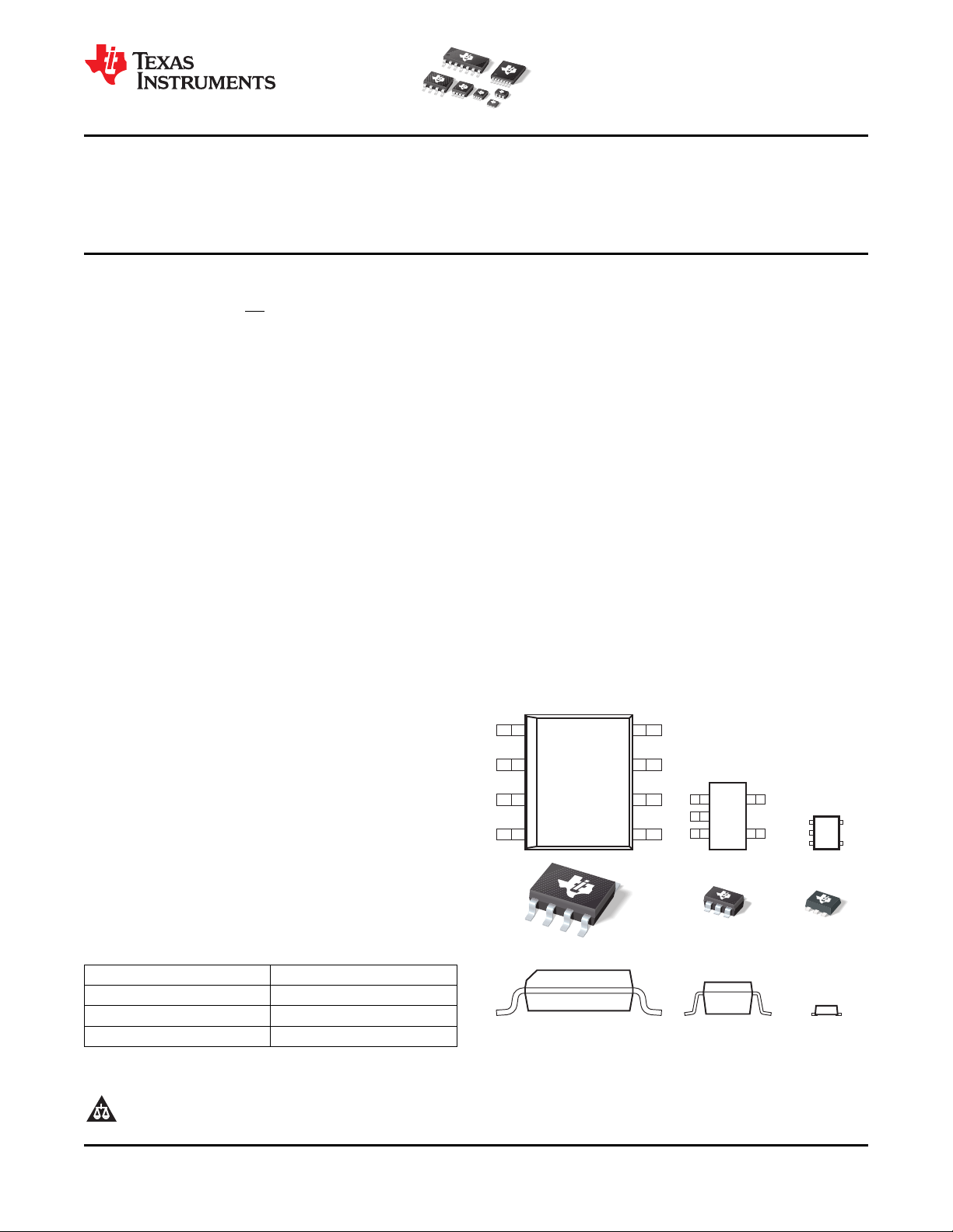
PackageFootprintComparison(toScale)
PackageHeight (toScale)Comparison
D(SO-8) DBV(SOT23-5) DRL(SOT553)
www.ti.com
36V, Single-Supply, SOT553, General-Purpose
OPERATIONAL AMPLIFIERS
Value Line Series
Check for Samples: OPA171, OPA2171, OPA4171
1
FEATURES
• Supply Range: +2.7V to +36V, ±1.35V to ±18V
• Low Noise: 14nV/√Hz
• Low Offset Drift: ±0.3µV/°C (typ)
• RFI Filtered Inputs
• Input Range Includes the Negative Supply
• Input Range Operates to Positive Supply
• Rail-to-Rail Output
• Gain Bandwidth: 3MHz
• Low Quiescent Current: 475µA per Amplifier
• High Common-Mode Rejection: 120dB (typ)
• Low Input Bias Current: 8pA
• Industry-Standard Packages:
– 8-Pin SOIC
– 8-Pin MSOP
– 14-Pin TSSOP
• microPackages:
– Single in SOT553
– Dual in VSSOP-8
OPA171
OPA2171
OPA4171
SBOS516D –SEPTEMBER 2010–REVISED SEPTEMBER 2012
DESCRIPTION
The OPA171, OPA2171 and OPA4171 (OPAx171)2
are a family of 36V, single-supply, low-noise
operational amplifiers with the ability to operate on
supplies ranging from +2.7V (±1.35V) to +36V
(±18V). These devices are available in micropackages and offer low offset, drift, and bandwidth
with low quiescent current. The single, dual, and
quad versions all have identical specifications for
maximum design flexibility.
Unlike most op amps, which are specified at only one
supply voltage, the OPAx171 family is specified from
+2.7V to +36V. Input signals beyond the supply rails
do not cause phase reversal. The OPAx171 family is
stable with capacitive loads up to 300pF. The input
can operate 100mV below the negative rail and within
2V of the top rail during normal operation. Note that
these devices can operate with full rail-to-rail input
100mV beyond the top rail, but with reduced
performance within 2V of the top rail.
The OPAx171 series of op amps are specified from
–40°C to +125°C.
APPLICATIONS
• Tracking Amplifier in Power Modules
• Merchant Power Supplies
• Transducer Amplifiers
• Bridge Amplifiers
• Temperature Measurements
• Strain Gauge Amplifiers
• Precision Integrators
• Battery-Powered Instruments
• Test Equipment
Product Family
DEVICE PACKAGE
OPA171 SOT553, SOT23-5, SO-8
OPA2171 (dual) VSSOP-8, SO-8, MSOP-8
OPA4171 (quad) TSSOP-14, SO-14
1
Please be aware that an important notice concerning availability, standard warranty, and use in critical applications of
Texas Instruments semiconductor products and disclaimers thereto appears at the end of this data sheet.
2All trademarks are the property of their respective owners.
PRODUCTION DATA information is current as of publication date.
Products conform to specifications per the terms of the Texas
Instruments standard warranty. Production processing does not
necessarily include testing of all parameters.
Smallest Packaging for 36V Op Amps
Copyright © 2010–2012, Texas Instruments Incorporated
OPA171
OPA2171
OPA4171
SBOS516D –SEPTEMBER 2010–REVISED SEPTEMBER 2012
This integrated circuit can be damaged by ESD. Texas Instruments recommends that all integrated circuits be handled with
appropriate precautions. Failure to observe proper handling and installation procedures can cause damage.
ESD damage can range from subtle performance degradation to complete device failure. Precision integrated circuits may be more
susceptible to damage because very small parametric changes could cause the device not to meet its published specifications.
www.ti.com
PACKAGE/ORDERING INFORMATION
PACKAGE PACKAGE TRANSPORT MEDIA,
PRODUCT PACKAGE-LEAD DESIGNATOR MARKING ORDERING NUMBER QUANTITY
SOT553 DRL DAP
OPA171 SOT23-5 DBV OSUI
SO-8 D O171A
MSOP-8 DGK OPMI
OPA2171 VSSOP-8 DCU OPOC
SO-8 D 2171A
SO-14 D OPA4171
OPA4171
TSSOP-14 PW OPA4171
(1) For the most current package and ordering information, see the Package Option Addendum at the end of this document, or visit the
device product folder at www.ti.com.
(1)
OPA171AIDRLT Tape and Reel, 250
OPA171AIDRLR Tape and Reel, 4000
OPA171AIDBVT Tape and Reel, 250
OPA171AIDBVR Tape and Reel, 3000
OPA171AID Rail, 75
OPA171AIDR Tape and Reel, 2500
OPA2171AIDGK Rail, 80
OPA2171AIDGKR Tape and Reel, 2500
OPA2171AIDCUT Tape and Reel, 250
OPA2171AIDCUR Tape and Reel, 3000
OPA2171AID Rail, 75
OPA2171AIDR Tape and Reel, 2500
OPA4171AID Rail, 50
OPA4171AIDR Tape and Reel, 2500
OPA4171AIPW Rail, 90
OPA4171AIPWR Tape and Reel, 2000
ABSOLUTE MAXIMUM RATINGS
(1)
Over operating free-air temperature range, unless otherwise noted.
OPAx171 UNIT
Supply voltage ±20 V
Signal input terminals
Output short circuit
Operating temperature –55 to +150 °C
Storage temperature –65 to +150 °C
Junction temperature +150 °C
ESD ratings:
(1) Stresses above these ratings may cause permanent damage. Exposure to absolute maximum conditions for extended periods may
degrade device reliability. These are stress ratings only, and functional operation of the device at these or any other conditions beyond
those specified is not implied.
(2) Short-circuit to ground, one amplifier per package.
Voltage (V–) – 0.5 to (V+) + 0.5 V
Current ±10 mA
(2)
Human body model (HBM) 4 kV
Charged device model (CDM) 750 V
Continuous
2 Submit Documentation Feedback Copyright © 2010–2012, Texas Instruments Incorporated
Product Folder Links: OPA171 OPA2171 OPA4171
OPA171
OPA2171
OPA4171
www.ti.com
ELECTRICAL CHARACTERISTICS
Boldface limits apply over the specified temperature range, TA= –40°C to +125°C.
At TA= +25°C, VS= +2.7V to +36V, VCM= V
PARAMETER TEST CONDITIONS MIN TYP MAX UNIT
OFFSET VOLTAGE
Input offset voltage V
Over temperature 0.3 ±2 mV
Drift dVOS/dT 0.3 ±2 µV/°C
vs power supply PSRR VS= +4V to +36V 1 ±3 µV/V
Channel separation, dc dc 5 µV/V
INPUT BIAS CURRENT
Input bias current I
Over temperature ±3.5 nA
Input offset current I
Over temperature ±3.5 nA
NOISE
Input voltage noise f = 0.1Hz to 10Hz 3 µV
Input voltage noise density e
INPUT VOLTAGE
Common-mode voltage range
Common-mode rejection ratio CMRR
INPUT IMPEDANCE
Differential 100 || 3 MΩ || pF
Common-mode 6 || 3
OPEN-LOOP GAIN
Open-loop voltage gain AOLVS= +4V to +36V, (V–) + 0.35V < VO< (V+) – 0.35V 110 130 dB
FREQUENCY RESPONSE
Gain bandwidth product GBP 3.0 MHz
Slew rate SR G = +1 1.5 V/µs
Settling time t
Overload recovery time VIN× Gain > V
Total harmonic distortion + noise THD+N G = +1, f = 1kHz, VO= 3V
OUTPUT
Voltage output swing from rail V
Over temperature RL= 10kΩ, AOL≥ 110dB (V–) + 0.35 (V+) – 0.35 V
Short-circuit current I
Capacitive load drive C
Open-loop output resistance R
POWER SUPPLY
Specified voltage range V
Quiescent current per amplifier I
Over temperature IO= 0A 650 µA
TEMPERATURE
Specified range –40 +125 °C
Operating range –55 +150 °C
(1)
(1) The input range can be extended beyond (V+) – 2V up to V+. See the Typical Characteristics and Application Information sections for
additional information.
OS
B
OS
n
V
CM
S
To 0.01% (12 bit), VS= ±18V, G = +1, 10V step 10 µs
O
SC
LOAD
O
S
Q
= VS/2, and R
OUT
f = 100Hz 25 nV/√Hz
f = 1kHz 14 nV/√Hz
VS= ±2V, (V–) – 0.1V < VCM< (V+) – 2V 90 104 dB
VS= ±18V, (V–) – 0.1V < VCM< (V+) – 2V 104 120 dB
To 0.1%, VS= ±18V, G = +1, 10V step 6 µs
VS= 5V, RL= 10kΩ 30 mV
f = 1MHz, IO= 0A 150 Ω
IO= 0A 475 595 µA
= 10kΩ connected to VS/2, unless otherwise noted.
LOAD
S
SBOS516D –SEPTEMBER 2010–REVISED SEPTEMBER 2012
OPA171, OPA2171, OPA4171
0.25 ±1.8 mV
±8 ±15 pA
±4 pA
(V–) – 0.1V (V+) – 2V V
2 µs
RMS
See Typical Characteristics pF
+2.7 +36 V
0.0002 %
+25/–35 mA
1012Ω ||
pF
PP
Copyright © 2010–2012, Texas Instruments Incorporated Submit Documentation Feedback 3
Product Folder Links: OPA171 OPA2171 OPA4171
OPA171
OPA2171
OPA4171
SBOS516D –SEPTEMBER 2010–REVISED SEPTEMBER 2012
THERMAL INFORMATION: OPA171
THERMAL METRIC
(1)
D (SO) DBV (SOT23) DRL (SOT553) UNITS
8 PINS 5 PINS 5 PINS
θ
JA
θ
JC(top)
θ
JB
ψ
JT
ψ
JB
θ
JC(bottom)
Junction-to-ambient thermal resistance 149.5 245.8 208.1
Junction-to-case(top) thermal resistance 97.9 133.9 0.1
Junction-to-board thermal resistance 87.7 83.6 42.4
Junction-to-top characterization parameter 35.5 18.2 0.5
Junction-to-board characterization parameter 89.5 83.1 42.2
Junction-to-case(bottom) thermal resistance N/A N/A N/A
(1) For more information about traditional and new thermal metrics, see the IC Package Thermal Metrics application report, SPRA953.
OPA171
THERMAL INFORMATION: OPA2171
THERMAL METRIC
(1)
D (SO) DCU (VSSOP) DGK (MSOP) UNITS
8 PINS 8 PINS 8 PINS
θ
JA
θ
JC(top)
θ
JB
ψ
JT
ψ
JB
θ
JC(bottom)
Junction-to-ambient thermal resistance 134.3 175.2 195.3
Junction-to-case(top) thermal resistance 72.1 74.9 59.4
Junction-to-board thermal resistance 60.6 22.2 115.1
Junction-to-top characterization parameter 18.2 1.6 4.7
Junction-to-board characterization parameter 53.8 22.8 114.4
Junction-to-case(bottom) thermal resistance N/A N/A N/A
(1) For more information about traditional and new thermal metrics, see the IC Package Thermal Metrics application report, SPRA953.
OPA2171
www.ti.com
°C/W
°C/W
THERMAL INFORMATION: OPA4171
THERMAL METRIC
(1)
D (SO) PW (TSSOP) UNITS
14 PINS 14 PINS
θ
JA
θ
JC(top)
θ
JB
ψ
JT
ψ
JB
θ
JC(bottom)
Junction-to-ambient thermal resistance 93.2 106.9
Junction-to-case(top) thermal resistance 51.8 24.4
Junction-to-board thermal resistance 49.4 59.3
Junction-to-top characterization parameter 13.5 0.6
Junction-to-board characterization parameter 42.2 54.3
Junction-to-case(bottom) thermal resistance N/A N/A
(1) For more information about traditional and new thermal metrics, see the IC Package Thermal Metrics application report, SPRA953.
OPA4171
°C/W
4 Submit Documentation Feedback Copyright © 2010–2012, Texas Instruments Incorporated
Product Folder Links: OPA171 OPA2171 OPA4171
1
2
3
4
8
7
6
5
NC
(1)
V+
OUT
NC
(1)
NC
(1)
-IN
+IN
V-
1
2
3
4
14
13
12
11
OUTD
-IND
+IND
V-
OUTA
-INA
+INA
V+
5
6
7
10
9
8
+INC
-INC
OUTC
+INB
-INB
OUTB
1
2
3
5
4
V+
-IN
OUT
V-
+IN
1
2
3
4
8
7
6
5
V+
OUTB
-INB
+INB
OUTA
-INA
+INA
V-
1
2
3
5
4
V+
OUT
IN+
V-
IN-
www.ti.com
OPA171
OPA2171
OPA4171
SBOS516D –SEPTEMBER 2010–REVISED SEPTEMBER 2012
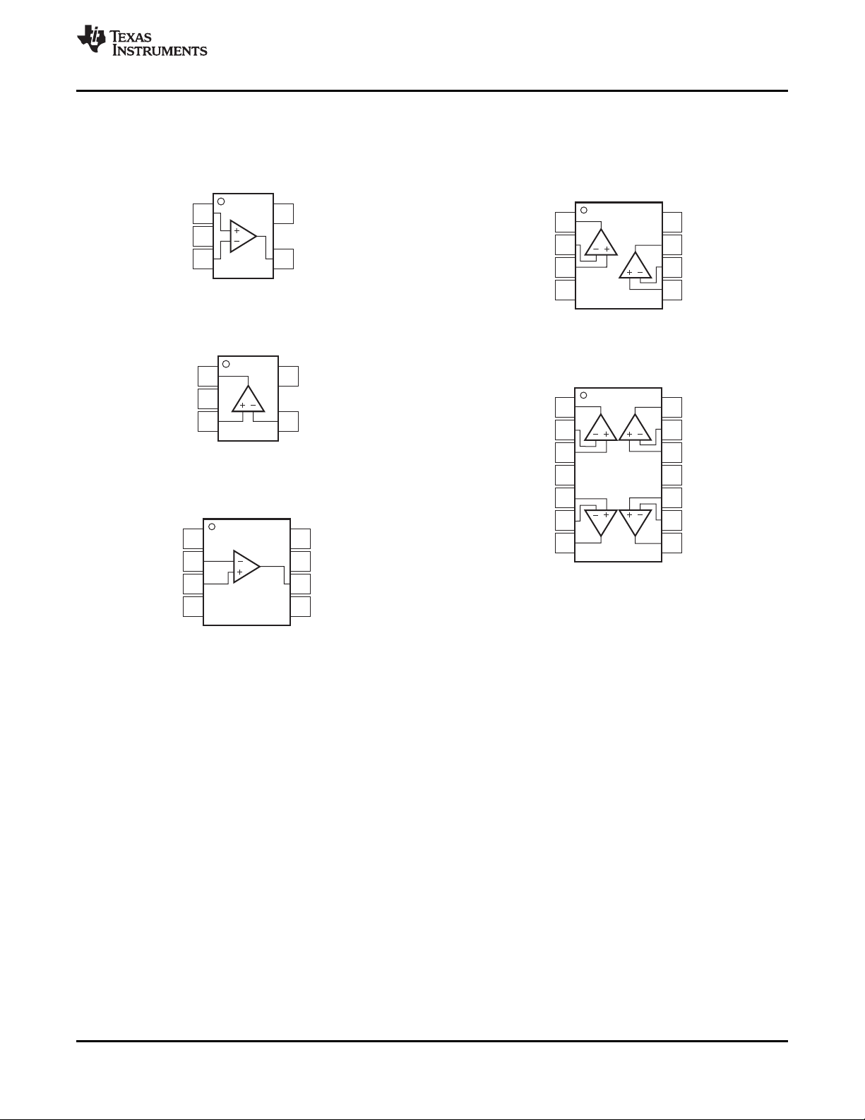
PIN CONFIGURATIONS
DRL PACKAGE: OPA171
SOT-553
(TOP VIEW)
DBV PACKAGE: OPA171
SOT23-5
(TOP VIEW)
D PACKAGE: OPA171
SO-8
(TOP VIEW)
D, DCU, AND DGK PACKAGES: OPA2171
SO-8, VSSOP-8, AND MSOP-8
(TOP VIEW)
D AND PW PACKAGES: OPA4171
SO-14 AND TSSOP-14
(TOP VIEW)
(1) No internal connection.
Product Folder Links: OPA171 OPA2171 OPA4171
Copyright © 2010–2012, Texas Instruments Incorporated Submit Documentation Feedback 5

OPA171
OPA2171
OPA4171
SBOS516D –SEPTEMBER 2010–REVISED SEPTEMBER 2012
TYPICAL CHARACTERISTICS
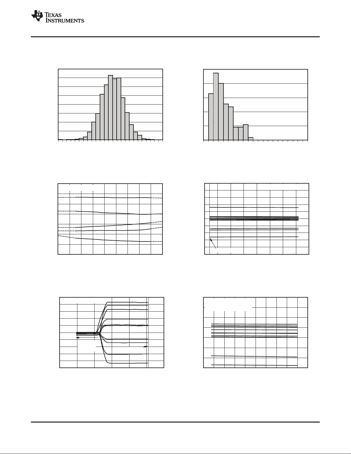
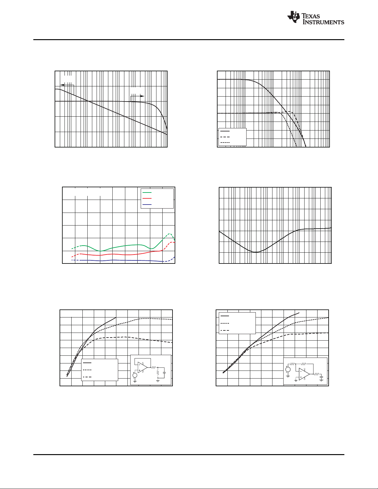
Table 1. Characteristic Performance Measurements
DESCRIPTION FIGURE
Offset Voltage Production Distribution Figure 1
Offset Voltage Drift Distribution Figure 2
Offset Voltage vs Temperature Figure 3
Offset Voltage vs Common-Mode Voltage Figure 4
Offset Voltage vs Common-Mode Voltage (Upper Stage) Figure 5
Offset Voltage vs Power Supply Figure 6
IBand IOSvs Common-Mode Voltage Figure 7
Input Bias Current vs Temperature Figure 8
Output Voltage Swing vs Output Current (Maximum Supply) Figure 9
CMRR and PSRR vs Frequency (Referred-to Input) Figure 10
CMRR vs Temperature Figure 11
PSRR vs Temperature Figure 12
0.1Hz to 10Hz Noise Figure 13
Input Voltage Noise Spectral Density vs Frequency Figure 14
THD+N Ratio vs Frequency Figure 15
THD+N vs Output Amplitude Figure 16
Quiescent Current vs Temperature Figure 17
Quiescent Current vs Supply Voltage Figure 18
Open-Loop Gain and Phase vs Frequency Figure 19
Closed-Loop Gain vs Frequency Figure 20
Open-Loop Gain vs Temperature Figure 21
Open-Loop Output Impedance vs Frequency Figure 22
Small-Signal Overshoot vs Capacitive Load (100mV Output Step) Figure 23, Figure 24
No Phase Reversal Figure 25
Positive Overload Recovery Figure 26
Negative Overload Recovery Figure 27
Small-Signal Step Response (100mV) Figure 28, Figure 29
Large-Signal Step Response Figure 30, Figure 31
Large-Signal Settling Time (10V Positive Step) Figure 32
Large-Signal Settling Time (10V Negative Step) Figure 33
Short-Circuit Current vs Temperature Figure 34
Maximum Output Voltage vs Frequency Figure 35
Channel Separation vs Frequency Figure 36
www.ti.com
6 Submit Documentation Feedback Copyright © 2010–2012, Texas Instruments Incorporated
Product Folder Links: OPA171 OPA2171 OPA4171
10000
8000
6000
4000
2000
0
2000
4000
6000
8000
10000
-
-
-
-
-
V ( V)m
OS
15.5 16 16.5 17 17.5 18 18.5
V (V)
CM
10TypicalUnitsShown
Normal
Operation
V =+18.1V
CM
350
250
150
50
50
150
250
350
-
-
-
-
V ( V)m
OS
0 2 4 6 8 16 20
V (V)
SUPPLY
V = 1.35Vto 18V
10TypicalUnitsShown
±
SUPPLY
±
18141210
600
400
200
0
200
400
600
800
-
-
-
-
OffsetVoltage( V)m
-75 -50 -25 0 25 150
Temperature( C)°
50 12510075
5TypicalUnitsShown
1000
800
600
400
200
0
200
400
600
800
1000
-
-
-
-
-
V ( V)m
OS
-20 -15 -10 -5 0 5 10 15 20
V (V)
CM
V = 18.1V-
CM
10TypicalUnitsShown
-1200
-1100
-1000
-900
-800
-700
-600
-500
-400
-300
-100
0
100
200
300
400
500
600
700
800
900
1000
1200
OffsetVoltage( V)m
PercentageofAmplifiers(%)
16
14
12
10
8
6
4
2
0
-200
1100
DistributionTakenFrom3500Amplifiers
0
0.1
0.2
0.3
0.4
0.5
0.6
0.7
0.8
0.9
1.1
1.2
1.3
2
OffsetVoltageDrift( V/ C)m °
PercentageofAmplifiers(%)
25
20
15
10
5
0
1
DistributionTakenFrom110Amplifiers
1.5
1.7
1.9
1.8
1.6
1.4
www.ti.com
OPA2171
OPA4171
SBOS516D –SEPTEMBER 2010–REVISED SEPTEMBER 2012
TYPICAL CHARACTERISTICS
VS= ±18V, VCM= VS/2, R
OFFSET VOLTAGE PRODUCTION DISTRIBUTION OFFSET VOLTAGE DRIFT DISTRIBUTION
Figure 1. Figure 2.
= 10kΩ connected to VS/2, and CL= 100pF, unless otherwise noted.
LOAD
OPA171
OFFSET VOLTAGE vs TEMPERATURE OFFSET VOLTAGE vs COMMON-MODE VOLTAGE
Figure 3. Figure 4.
OFFSET VOLTAGE vs COMMON-MODE VOLTAGE
(Upper Stage) OFFSET VOLTAGE vs POWER SUPPLY
Copyright © 2010–2012, Texas Instruments Incorporated Submit Documentation Feedback 7
Figure 5. Figure 6.
Product Folder Links: OPA171 OPA2171 OPA4171
30
20
10
0
10
20
30
-
-
-
Common-ModeRejectionRatio( V/V)m
-75 -50 -25 0 25 150
Temperature( C)°
50 12510075
V =2.7V
S
V =4V
S
V =36V
S
3
2
1
0
1
2
3
-
-
-
Power-SupplyRejectionRatio( V/V)m
-75 -50 -25 0 25 150
Temperature( C)°
50 12510075
V =2.7Vto36V
S
V =4Vto36V
S
18
OutputVoltage(V)
0 2 4 6 8 16
OutputCurrent(mA)
10 12 14
17
16
15
14.5
-14.5
-15
-16
-17
-18
- °40 C
+25 C°
+85 C°
+125 C°
140
120
100
80
60
40
20
0
Common-ModeRejectionRatio(dB),
Power-SupplyRejectionRatio(dB)
1 10 100 1k 10k 10M
Frequency(Hz)
100k 1M
+PSRR
-PSRR
CMRR
15
14
13
12
11
10
9
8
7
6
5
4
3
2
1
0
I andI (pA)
B OS
-20 -12 -6 0 6 20
V (V)
CM
12
-I
B
+I
B
-I
OS
-18 18
V = 18.1V-
CM
V =16V
CM
I
B+
I
B-
I
OS
10000
1000
100
10
1
0
InputBiasCurrent(pA)
-75 -50 -25 0 25 150
Temperature( C)°
50 12510075
I
B
I
OS
OPA171
OPA2171
OPA4171
SBOS516D –SEPTEMBER 2010–REVISED SEPTEMBER 2012
TYPICAL CHARACTERISTICS (continued)
VS= ±18V, VCM= VS/2, R
IBAND IOSvs COMMON-MODE VOLTAGE INPUT BIAS CURRENT vs TEMPERATURE
OUTPUT VOLTAGE SWING vs OUTPUT CURRENT CMRR AND PSRR vs FREQUENCY
= 10kΩ connected to VS/2, and CL= 100pF, unless otherwise noted.
LOAD
Figure 7. Figure 8.
(Maximum Supply) (Referred-to Input)
www.ti.com
Figure 9. Figure 10.
CMRR vs TEMPERATURE PSRR vs TEMPERATURE
8 Submit Documentation Feedback Copyright © 2010–2012, Texas Instruments Incorporated
Figure 11. Figure 12.
Product Folder Links: OPA171 OPA2171 OPA4171
0.65
0.6
0.55
0.5
0.45
0.4
0.35
I (mA)
Q
-75 -50 -25 0 25 150
Temperature( C)°
1251007550
0.6
0.55
0.5
0.45
0.4
0.35
0.3
0.25
I (mA)
Q
0 4 8 12 16 36
SupplyVoltage(V)
32282420
SpecifiedSupply-VoltageRange
0.01
0.001
0.0001
0.00001
TotalHarmonicDistortion+Noise(%)
10 100 1k 10k 20k
Frequency(Hz)
TotalHarmonicDistortion+Noise(dB)
V =3V
BW=80kHz
OUT RMS
G=+1,R =10kW
L
G= 1,R =2k- W
L
-80
-100
-120
-140
0.1
0.01
0.001
0.0001
0.00001
TotalHarmonicDistortion+Noise(%)
0.01 0.1 1 10 20
OutputAmplitude(V )
RMS
-80
TotalHarmonicDistortion+Noise(dB)
BW=80kHz
G=+1,R =10kW
L
G= 1,R =2k- W
L
-100
-120
-140
1000
100
10
1
VoltageNoiseDensity(nV/ )Ö
Hz
1 10 100 1k 10k 1M
Frequency(Hz)
100k
1 V/divm
Time(1s/div)
www.ti.com
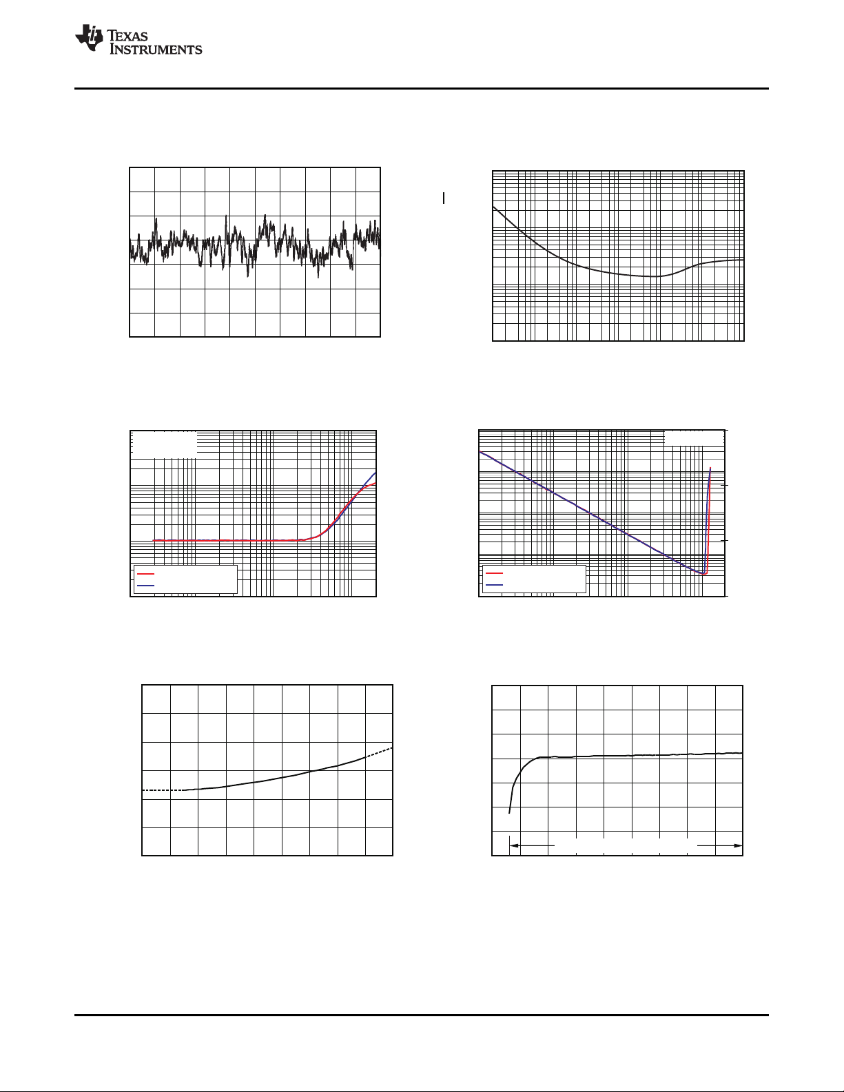
VS= ±18V, VCM= VS/2, R
THD+N RATIO vs FREQUENCY THD+N vs OUTPUT AMPLITUDE
SBOS516D –SEPTEMBER 2010–REVISED SEPTEMBER 2012
TYPICAL CHARACTERISTICS (continued)
= 10kΩ connected to VS/2, and CL= 100pF, unless otherwise noted.
LOAD
0.1Hz TO 10Hz NOISE FREQUENCY
Figure 13. Figure 14.
INPUT VOLTAGE NOISE SPECTRAL DENSITY vs
OPA171
OPA2171
OPA4171
QUIESCENT CURRENT vs TEMPERATURE QUIESCENT CURRENT vs SUPPLY VOLTAGE
Copyright © 2010–2012, Texas Instruments Incorporated Submit Documentation Feedback 9
Figure 15. Figure 16.
Figure 17. Figure 18.
Product Folder Links: OPA171 OPA2171 OPA4171
50
45
40
35
30
25
20
15
10
5
0
Overshoot(%)
0 100 200 300 400 500 600 700 800 900 1000
CapacitiveLoad(pF)
+18V
-18V
R
OUT
C
L
OPA171
R
L
G=+1
R =0W
OUT
R =25W
OUT
R =50W
OUT
R =10kW
L
50
45
40
35
30
25
20
15
10
5
0
Overshoot(%)
0 100 200 300 400 500 600 700 800 900 1000
CapacitiveLoad(pF)
OPA171
R =I10kW
R
OUT
C
L
RF=10kW
+18V
-18V
G= 1-
R =0W
OUT
R =25W
OUT
R =50W
OUT
3
2.5
2
1.5
1
0.5
0
A ( V/V)m
OL
-75 150
Temperature( C)°
-25-50 0
5TypicalUnitsShown
125100755025
V =2.7V
S
V =4V
S
V =36V
S
1M
100k
10k
1k
100
10
1
1m
Z ( )W
O
1 10 100 1k 10k 10M
Frequency(Hz)
100k 1M
180
135
90
45
0
45-
Gain(dB)
1 10 100 1k 10k 10M
Frequency(Hz)
1M100k
Phase
Gain
Phase( )°
180
135
90
45
0
-45
25
20
15
10
5
0
5
10
15
20
-
-
-
-
Gain(dB)
10k 100M
Frequency(Hz)
1M100k 10M
G=10
G=1
G= 1-
OPA171
OPA2171
OPA4171
SBOS516D –SEPTEMBER 2010–REVISED SEPTEMBER 2012
TYPICAL CHARACTERISTICS (continued)
VS= ±18V, VCM= VS/2, R
OPEN-LOOP GAIN AND PHASE vs FREQUENCY CLOSED-LOOP GAIN vs FREQUENCY
OPEN-LOOP GAIN vs TEMPERATURE OPEN-LOOP OUTPUT IMPEDANCE vs FREQUENCY
= 10kΩ connected to VS/2, and CL= 100pF, unless otherwise noted.
LOAD
Figure 19. Figure 20.
www.ti.com
Figure 21. Figure 22.
SMALL-SIGNAL OVERSHOOT vs CAPACITIVE LOAD SMALL-SIGNAL OVERSHOOT vs CAPACITIVE LOAD
(100mV Output Step) (100mV Output Step)
10 Submit Documentation Feedback Copyright © 2010–2012, Texas Instruments Incorporated
Figure 23. Figure 24.
Product Folder Links: OPA171 OPA2171 OPA4171
Time(20 s/div)m
20mV/div
+18V
-18V
R 2kW
F
=
R 2kW
I
=
C
L
OPA171
G= 1-
C =100pF
L
2V/div
Time(5 s/div)m
G=+1
R =10k
C =100pF
W
L
L
Time(5 s/div)m
5V/div
V
IN
V
OUT
2kW
20kW
V
IN
V
OUT
OPA171
G= 10-
+18V
-18V
20mV/div
Time(1 s/div)m
+18V
-18V
C
L
R
L
OPA171
G=+1
R =10k
C =100pF
W
L
L
Output
Output
Time(100 s/div)m
5V/div
+18V
-18V
37V
PP
SineWave
( 18.5V)±
OPA171
Time(5 s/div)m
5V/div
V
IN
V
OUT
2kW
20kW
V
IN
V
OUT
OPA171
G= 10-
+18V
-18V
www.ti.com
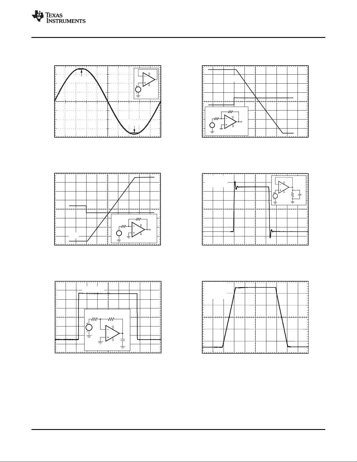
VS= ±18V, VCM= VS/2, R
NO PHASE REVERSAL POSITIVE OVERLOAD RECOVERY
NEGATIVE OVERLOAD RECOVERY (100mV)
SBOS516D –SEPTEMBER 2010–REVISED SEPTEMBER 2012
TYPICAL CHARACTERISTICS (continued)
= 10kΩ connected to VS/2, and CL= 100pF, unless otherwise noted.
LOAD
Figure 25. Figure 26.
SMALL-SIGNAL STEP RESPONSE
OPA171
OPA2171
OPA4171
Figure 27. Figure 28.
SMALL-SIGNAL STEP RESPONSE
(100mV) LARGE-SIGNAL STEP RESPONSE
Figure 29. Figure 30.
Copyright © 2010–2012, Texas Instruments Incorporated Submit Documentation Feedback 11
Product Folder Links: OPA171 OPA2171 OPA4171

15
12.5
10
7.5
5
2.5
0
OutputVoltage(V )
PP
10k 100k 1M 10M
Frequency(Hz)
V = 15V±
S
V = 5V±
S
V = 1.35V±
S
Maximumoutputvoltagewithout
slew-rateinduceddistortion.
-60
70
80
90
100
110
120
-
-
-
-
-
-
ChannelSeparation(dB)
10 100 1k 10k 100k
Frequency(Hz)
10
8
6
4
2
0
2
4
6
8
10
-
-
-
-
-
D FromFinalValue(mV)
0 36
Time( s)m
84 28 3224201612
12-BitSettling
( 1/2LSB= 0.024%)± ±
G= 1-
50
45
40
35
30
25
20
15
10
5
0
I (mA)
SC
-75 -50 -25 0 25 150
Temperature( C)°
50 125
I ,Source
SC
10075
I ,Sink
SC
10
8
6
4
2
0
2
4
6
8
10
-
-
-
-
-
D FromFinalValue(mV)
0 36
Time( s)m
84 28 3224201612
12-BitSettling
( 1/2LSB= 0.024%)± ±
G= 1-
Time(4 s/div)m
2V/div
G= 1
R =10k
C =100pF
W
L
L
OPA171
OPA2171
OPA4171
SBOS516D –SEPTEMBER 2010–REVISED SEPTEMBER 2012
TYPICAL CHARACTERISTICS (continued)
VS= ±18V, VCM= VS/2, R
LARGE-SIGNAL STEP RESPONSE (10V Positive Step)
LARGE-SIGNAL SETTLING TIME
= 10kΩ connected to VS/2, and CL= 100pF, unless otherwise noted.
LOAD
Figure 31. Figure 32.
(10V Negative Step) SHORT-CIRCUIT CURRENT vs TEMPERATURE
www.ti.com
LARGE-SIGNAL SETTLING TIME
Figure 33. Figure 34.
MAXIMUM OUTPUT VOLTAGE vs FREQUENCY CHANNEL SEPARATION vs FREQUENCY
12 Submit Documentation Feedback Copyright © 2010–2012, Texas Instruments Incorporated
Figure 35. Figure 36.
Product Folder Links: OPA171 OPA2171 OPA4171

Output
Output
Time(100 s/div)m
5V/div
+18V
-18V
37V
PP
SineWave
( 18.5V)±
OPA171
OPA171
OPA2171
OPA4171
www.ti.com
APPLICATION INFORMATION
The OPAx171 family of operational amplifiers provide This device can operate with full rail-to-rail input
high overall performance, making them ideal for many 100mV beyond the top rail, but with reduced
general-purpose applications. The excellent offset performance within 2V of the top rail. The typical
drift of only 2µV/°C provides excellent stability over performance in this range is summarized in Table 2.
the entire temperature range. In addition, the device
offers very good overall performance with high
CMRR, PSRR, and AOL. As with all amplifiers,
applications with noisy or high-impedance power
supplies require decoupling capacitors close to the
device pins. In most cases, 0.1µF capacitors are
adequate.
OPERATING CHARACTERISTICS
The OPAx171 family of amplifiers is specified for The input of the OPAx171 prevents phase reversal
operation from 2.7V to 36V (±1.35V to ±18V). Many with excessive common-mode voltage. Instead, the
of the specifications apply from –40°C to +125°C. output limits into the appropriate rail. This
Parameters that can exhibit significant variance with performance is shown in Figure 37.
regard to operating voltage or temperature are
presented in the Typical Characteristics.
PHASE-REVERSAL PROTECTION
The OPAx171 family has an internal phase-reversal
protection. Many op amps exhibit a phase reversal
when the input is driven beyond its linear commonmode range. This condition is most often encountered
in noninverting circuits when the input is driven
beyond the specified common-mode voltage range,
causing the output to reverse into the opposite rail.
SBOS516D –SEPTEMBER 2010–REVISED SEPTEMBER 2012
GENERAL LAYOUT GUIDELINES
For best operational performance of the device, good
printed circuit board (PCB) layout practices are
recommended. Low-loss, 0.1µF bypass capacitors
should be connected between each supply pin and
ground, placed as close to the device as possible. A
single bypass capacitor from V+ to ground is
applicable to single-supply applications.
COMMON-MODE VOLTAGE RANGE
The input common-mode voltage range of the
OPAx171 series extends 100mV below the negative
rail and within 2V of the top rail for normal operation.
Table 2. Typical Performance Range
PARAMETER MIN TYP MAX UNIT
Input Common-Mode Voltage (V+) – 2 (V+) + 0.1 V
Offset voltage 7 mV
vs Temperature 12 µV/°C
Common-mode rejection 65 dB
Open-loop gain 60 dB
GBW 0.7 MHz
Slew rate 0.7 V/µs
Noise at f = 1kHz 30 nV/√Hz
Figure 37. No Phase Reversal
Product Folder Links: OPA171 OPA2171 OPA4171
Copyright © 2010–2012, Texas Instruments Incorporated Submit Documentation Feedback 13

50
45
40
35
30
25
20
15
10
5
0
Overshoot(%)
0 100 200 300 400 500 600 700 800 900 1000
CapacitiveLoad(pF)
OPA171
R =I10kW
R
OUT
C
L
RF=10kW
+18V
-18V
G= 1-
R =0W
OUT
R =25W
OUT
R =50W
OUT
50
45
40
35
30
25
20
15
10
5
0
Overshoot(%)
0 100 200 300 400 500 600 700 800 900 1000
CapacitiveLoad(pF)
+18V
-18V
R
OUT
C
L
OPA171
R
L
G=+1
R =0W
OUT
R =25W
OUT
R =50W
OUT
R =10kW
L
5kW
OPA171
10mAmax
V+
V
IN
V
OUT
I
OVERLOAD
OPA171
OPA2171
OPA4171
SBOS516D –SEPTEMBER 2010–REVISED SEPTEMBER 2012
CAPACITIVE LOAD AND STABILITY or even the output pin. Each of these different pin
The dynamic characteristics of the OPAx171 have
been optimized for commonly encountered operating
conditions. The combination of low closed-loop gain
and high capacitive loads decreases the phase
margin of the amplifier and can lead to gain peaking
or oscillations. As a result, heavier capacitive loads
must be isolated from the output. The simplest way to
achieve this isolation is to add a small resistor (for
example, R
equal to 50Ω) in series with the These ESD protection diodes also provide in-circuit,
OUT
output. Figure 38 and Figure 39 illustrate graphs of input overdrive protection, as long as the current is
small-signal overshoot versus capacitive load for limited to 10mA as stated in the Absolute Maximum
several values of R
. Also, refer to Applications Ratings. Figure 40 shows how a series input resistor
OUT
Bulletin AB-028 (SBOA015), available for download may be added to the driven input to limit the input
from the TI website for details of analysis techniques current. The added resistor contributes thermal noise
and application circuits. at the amplifier input and its value should be kept to a
functions have electrical stress limits determined by
the voltage breakdown characteristics of the
particular semiconductor fabrication process and
specific circuits connected to the pin. Additionally,
internal electrostatic discharge (ESD) protection is
built into these circuits to protect them from
accidental ESD events both before and during
product assembly.
minimum in noise-sensitive applications.
www.ti.com
Figure 38. Small-Signal Overshoot versus
Capacitive Load (100mV Output Step)
Figure 39. Small-Signal Overshoot versus
Capacitive Load (100mV Output Step)
ELECTRICAL OVERSTRESS
Designers often ask questions about the capability of
an operational amplifier to withstand electrical
overstress. These questions tend to focus on the
device inputs, but may involve the supply voltage pins
14 Submit Documentation Feedback Copyright © 2010–2012, Texas Instruments Incorporated
An ESD event produces a short duration, highvoltage pulse that is transformed into a short
duration, high-current pulse as it discharges through
a semiconductor device. The ESD protection circuits
are designed to provide a current path around the
operational amplifier core to prevent it from being
damaged. The energy absorbed by the protection
circuitry is then dissipated as heat.
When the operational amplifier connects into a circuit,
the ESD protection components are intended to
remain inactive and not become involved in the
application circuit operation. However, circumstances
may arise where an applied voltage exceeds the
operating voltage range of a given pin. Should this
condition occur, there is a risk that some of the
internal ESD protection circuits may be biased on,
and conduct current. Any such current flow occurs
through ESD cells and rarely involves the absorption
device.
If there is an uncertainty about the ability of the
supply to absorb this current, external zener diodes
may be added to the supply pins. The zener voltage
must be selected such that the diode does not turn
on during normal operation.
However, its zener voltage should be low enough so
that the zener diode conducts if the supply pin begins
to rise above the safe operating supply voltage level.
Product Folder Links: OPA171 OPA2171 OPA4171
Figure 40. Input Current Protection

OPA171
OPA2171
OPA4171
www.ti.com
REVISION HISTORY
NOTE: Page numbers for previous revisions may differ from page numbers in the current version.
Changes from Revision C (June 2011) to Revision D Page
• Added "Value Line Series" to title ......................................................................................................................................... 1
Changes from Revision B (November 2010) to Revision C Page
• Added MSOP-8 package to device graphic .......................................................................................................................... 1
• Added MSOP-8 package to Features bullets ....................................................................................................................... 1
• Added MSOP-8 package to Product Family table ................................................................................................................ 1
• Added MSOP-8 package to Package/Ordering Information table ........................................................................................ 2
• Deleted "A" suffix from OPA4171 package markings in Package/Ordering Information table. ............................................ 2
• Added new row for Voltage Output Swing from Rail parameter to Output subsection of Electrical Characteristics ............ 3
• Changed Voltage Output Swing from Rail parameter to over temperature in Output subsection of Electrical
Characteristics ...................................................................................................................................................................... 3
• Updated format of thermal information tables ...................................................................................................................... 4
• Added MSOP-8 package to OPA2171 Thermal Information table ....................................................................................... 4
• Updated pinout configurations for OPA2171 and OPA4171 ................................................................................................ 5
• Changed Figure 9 ................................................................................................................................................................. 8
SBOS516D –SEPTEMBER 2010–REVISED SEPTEMBER 2012
Changes from Revision A (November, 2010) to Revision B Page
• Changed input offset voltage specification ........................................................................................................................... 3
• Changed input offset voltage, over temperature specification .............................................................................................. 3
• Changed quiescent current per amplifier, over temperature specification ........................................................................... 3
Copyright © 2010–2012, Texas Instruments Incorporated Submit Documentation Feedback 15
Product Folder Links: OPA171 OPA2171 OPA4171

PACKAGE OPTION ADDENDUM
www.ti.com
PACKAGING INFORMATION
Orderable Device Status
OPA171AID ACTIVE SOIC D 8 75 Green (RoHS
OPA171AIDBVR ACTIVE SOT-23 DBV 5 3000 Green (RoHS
OPA171AIDBVT ACTIVE SOT-23 DBV 5 250 Green (RoHS
OPA171AIDR ACTIVE SOIC D 8 2500 Green (RoHS
OPA171AIDRLR ACTIVE SOT DRL 5 4000 Green (RoHS
OPA171AIDRLT ACTIVE SOT DRL 5 250 Green (RoHS
OPA2171AID ACTIVE SOIC D 8 75 Green (RoHS
OPA2171AIDCUR ACTIVE US8 DCU 8 3000 Green (RoHS
OPA2171AIDCUT ACTIVE US8 DCU 8 250 Green (RoHS
OPA2171AIDGK ACTIVE VSSOP DGK 8 80 Green (RoHS
OPA2171AIDGKR ACTIVE VSSOP DGK 8 2500 Green (RoHS
OPA2171AIDR ACTIVE SOIC D 8 2500 Green (RoHS
OPA4171AID ACTIVE SOIC D 14 50 Green (RoHS
OPA4171AIDR ACTIVE SOIC D 14 2500 Green (RoHS
OPA4171AIPW ACTIVE TSSOP PW 14 90 Green (RoHS
OPA4171AIPWR ACTIVE TSSOP PW 14 2000 Green (RoHS
(1)
The marketing status values are defined as follows:
ACTIVE: Product device recommended for new designs.
Package Type Package
(1)
Drawing
Pins Package
Qty
Eco Plan
(2)
& no Sb/Br)
& no Sb/Br)
& no Sb/Br)
& no Sb/Br)
& no Sb/Br)
& no Sb/Br)
& no Sb/Br)
& no Sb/Br)
& no Sb/Br)
& no Sb/Br)
& no Sb/Br)
& no Sb/Br)
& no Sb/Br)
& no Sb/Br)
& no Sb/Br)
& no Sb/Br)
Lead/Ball Finish
(6)
MSL Peak Temp
(3)
Op Temp (°C) Device Marking
CU NIPDAU Level-2-260C-1 YEAR -40 to 125 O171A
CU NIPDAU Level-2-260C-1 YEAR -40 to 125 OSUI
CU NIPDAU Level-2-260C-1 YEAR -40 to 125 OSUI
CU NIPDAU Level-2-260C-1 YEAR -40 to 125 O171A
CU NIPDAU Level-1-260C-UNLIM -40 to 125 DAP
CU NIPDAU Level-1-260C-UNLIM -40 to 125 DAP
CU NIPDAU Level-2-260C-1 YEAR -40 to 125 2171A
CU NIPDAU Level-1-260C-UNLIM -40 to 125 OPOC
CU NIPDAU Level-1-260C-UNLIM -40 to 125 OPOC
CU NIPDAU |
Level-2-260C-1 YEAR -40 to 125 OPMI
CU NIPDAUAG
CU NIPDAU |
Level-2-260C-1 YEAR -40 to 125 OPMI
CU NIPDAUAG
CU NIPDAU Level-2-260C-1 YEAR -40 to 125 2171A
CU NIPDAU Level-3-260C-168 HR -40 to 125 OPA4171
CU NIPDAU Level-3-260C-168 HR -40 to 125 OPA4171
CU NIPDAU Level-2-260C-1 YEAR -40 to 125 OPA4171
CU NIPDAU Level-2-260C-1 YEAR -40 to 125 OPA4171
18-Oct-2013
Samples
(4/5)
Addendum-Page 1

PACKAGE OPTION ADDENDUM
www.ti.com
LIFEBUY: TI has announced that the device will be discontinued, and a lifetime-buy period is in effect.
NRND: Not recommended for new designs. Device is in production to support existing customers, but TI does not recommend using this part in a new design.
PREVIEW: Device has been announced but is not in production. Samples may or may not be available.
OBSOLETE: TI has discontinued the production of the device.
18-Oct-2013
(2)
Eco Plan - The planned eco-friendly classification: Pb-Free (RoHS), Pb-Free (RoHS Exempt), or Green (RoHS & no Sb/Br) - please check http://www.ti.com/productcontent for the latest availability
information and additional product content details.
TBD: The Pb-Free/Green conversion plan has not been defined.
Pb-Free (RoHS): TI's terms "Lead-Free" or "Pb-Free" mean semiconductor products that are compatible with the current RoHS requirements for all 6 substances, including the requirement that
lead not exceed 0.1% by weight in homogeneous materials. Where designed to be soldered at high temperatures, TI Pb-Free products are suitable for use in specified lead-free processes.
Pb-Free (RoHS Exempt): This component has a RoHS exemption for either 1) lead-based flip-chip solder bumps used between the die and package, or 2) lead-based die adhesive used between
the die and leadframe. The component is otherwise considered Pb-Free (RoHS compatible) as defined above.
Green (RoHS & no Sb/Br): TI defines "Green" to mean Pb-Free (RoHS compatible), and free of Bromine (Br) and Antimony (Sb) based flame retardants (Br or Sb do not exceed 0.1% by weight
in homogeneous material)
(3)
MSL, Peak Temp. - The Moisture Sensitivity Level rating according to the JEDEC industry standard classifications, and peak solder temperature.
(4)
There may be additional marking, which relates to the logo, the lot trace code information, or the environmental category on the device.
(5)
Multiple Device Markings will be inside parentheses. Only one Device Marking contained in parentheses and separated by a "~" will appear on a device. If a line is indented then it is a continuation
of the previous line and the two combined represent the entire Device Marking for that device.
(6)
Lead/Ball Finish - Orderable Devices may have multiple material finish options. Finish options are separated by a vertical ruled line. Lead/Ball Finish values may wrap to two lines if the finish
value exceeds the maximum column width.
Important Information and Disclaimer:The information provided on this page represents TI's knowledge and belief as of the date that it is provided. TI bases its knowledge and belief on information
provided by third parties, and makes no representation or warranty as to the accuracy of such information. Efforts are underway to better integrate information from third parties. TI has taken and
continues to take reasonable steps to provide representative and accurate information but may not have conducted destructive testing or chemical analysis on incoming materials and chemicals.
TI and TI suppliers consider certain information to be proprietary, and thus CAS numbers and other limited information may not be available for release.
In no event shall TI's liability arising out of such information exceed the total purchase price of the TI part(s) at issue in this document sold by TI to Customer on an annual basis.
OTHER QUALIFIED VERSIONS OF OPA171 :
Automotive: OPA171-Q1
•
NOTE: Qualified Version Definitions:
Automotive - Q100 devices qualified for high-reliability automotive applications targeting zero defects
•
Addendum-Page 2

PACKAGE MATERIALS INFORMATION
www.ti.com 18-Sep-2013
TAPE AND REEL INFORMATION
*All dimensions are nominal
Device Package
Type
OPA171AIDBVR SOT-23 DBV 5 3000 179.0 8.4 3.2 3.2 1.4 4.0 8.0 Q3
OPA171AIDBVR SOT-23 DBV 5 3000 180.0 8.4 3.23 3.17 1.37 4.0 8.0 Q3
OPA171AIDBVT SOT-23 DBV 5 250 180.0 8.4 3.23 3.17 1.37 4.0 8.0 Q3
OPA171AIDBVT SOT-23 DBV 5 250 179.0 8.4 3.2 3.2 1.4 4.0 8.0 Q3
OPA171AIDRLR SOT DRL 5 4000 180.0 8.4 1.98 1.78 0.69 4.0 8.0 Q3
OPA171AIDRLT SOT DRL 5 250 180.0 8.4 1.98 1.78 0.69 4.0 8.0 Q3
OPA2171AIDCUR US8 DCU 8 3000 180.0 8.4 2.25 3.35 1.05 4.0 8.0 Q3
OPA2171AIDCUT US8 DCU 8 250 180.0 8.4 2.25 3.35 1.05 4.0 8.0 Q3
OPA2171AIDGKR VSSOP DGK 8 2500 330.0 12.4 5.3 3.4 1.4 8.0 12.0 Q1
OPA2171AIDGKR VSSOP DGK 8 2500 330.0 12.4 5.3 3.4 1.4 8.0 12.0 Q1
OPA2171AIDR SOIC D 8 2500 330.0 12.4 6.4 5.2 2.1 8.0 12.0 Q1
OPA4171AIPWR TSSOP PW 14 2000 330.0 12.4 6.9 5.6 1.6 8.0 12.0 Q1
Package
Drawing
Pins SPQ Reel
Diameter
(mm)
Reel
Width
W1 (mm)
A0
(mm)B0(mm)K0(mm)P1(mm)W(mm)
Pin1
Quadrant
Pack Materials-Page 1

PACKAGE MATERIALS INFORMATION
www.ti.com 18-Sep-2013
*All dimensions are nominal
Device Package Type Package Drawing Pins SPQ Length (mm) Width (mm) Height (mm)
OPA171AIDBVR SOT-23 DBV 5 3000 195.0 200.0 45.0
OPA171AIDBVR SOT-23 DBV 5 3000 202.0 201.0 28.0
OPA171AIDBVT SOT-23 DBV 5 250 202.0 201.0 28.0
OPA171AIDBVT SOT-23 DBV 5 250 195.0 200.0 45.0
OPA171AIDRLR SOT DRL 5 4000 202.0 201.0 28.0
OPA171AIDRLT SOT DRL 5 250 202.0 201.0 28.0
OPA2171AIDCUR US8 DCU 8 3000 202.0 201.0 28.0
OPA2171AIDCUT US8 DCU 8 250 202.0 201.0 28.0
OPA2171AIDGKR VSSOP DGK 8 2500 366.0 364.0 50.0
OPA2171AIDGKR VSSOP DGK 8 2500 358.0 335.0 35.0
OPA2171AIDR SOIC D 8 2500 367.0 367.0 35.0
OPA4171AIPWR TSSOP PW 14 2000 367.0 367.0 35.0
Pack Materials-Page 2


IMPORTANT NOTICE
Texas Instruments Incorporated and its subsidiaries (TI) reserve the right to make corrections, enhancements, improvements and other
changes to its semiconductor products and services per JESD46, latest issue, and to discontinue any product or service per JESD48, latest
issue. Buyers should obtain the latest relevant information before placing orders and should verify that such information is current and
complete. All semiconductor products (also referred to herein as “components”) are sold subject to TI’s terms and conditions of sale
supplied at the time of order acknowledgment.
TI warrants performance of its components to the specifications applicable at the time of sale, in accordance with the warranty in TI’s terms
and conditions of sale of semiconductor products. Testing and other quality control techniques are used to the extent TI deems necessary
to support this warranty. Except where mandated by applicable law, testing of all parameters of each component is not necessarily
performed.
TI assumes no liability for applications assistance or the design of Buyers’ products. Buyers are responsible for their products and
applications using TI components. To minimize the risks associated with Buyers’ products and applications, Buyers should provide
adequate design and operating safeguards.
TI does not warrant or represent that any license, either express or implied, is granted under any patent right, copyright, mask work right, or
other intellectual property right relating to any combination, machine, or process in which TI components or services are used. Information
published by TI regarding third-party products or services does not constitute a license to use such products or services or a warranty or
endorsement thereof. Use of such information may require a license from a third party under the patents or other intellectual property of the
third party, or a license from TI under the patents or other intellectual property of TI.
Reproduction of significant portions of TI information in TI data books or data sheets is permissible only if reproduction is without alteration
and is accompanied by all associated warranties, conditions, limitations, and notices. TI is not responsible or liable for such altered
documentation. Information of third parties may be subject to additional restrictions.
Resale of TI components or services with statements different from or beyond the parameters stated by TI for that component or service
voids all express and any implied warranties for the associated TI component or service and is an unfair and deceptive business practice.
TI is not responsible or liable for any such statements.
Buyer acknowledges and agrees that it is solely responsible for compliance with all legal, regulatory and safety-related requirements
concerning its products, and any use of TI components in its applications, notwithstanding any applications-related information or support
that may be provided by TI. Buyer represents and agrees that it has all the necessary expertise to create and implement safeguards which
anticipate dangerous consequences of failures, monitor failures and their consequences, lessen the likelihood of failures that might cause
harm and take appropriate remedial actions. Buyer will fully indemnify TI and its representatives against any damages arising out of the use
of any TI components in safety-critical applications.
In some cases, TI components may be promoted specifically to facilitate safety-related applications. With such components, TI’s goal is to
help enable customers to design and create their own end-product solutions that meet applicable functional safety standards and
requirements. Nonetheless, such components are subject to these terms.
No TI components are authorized for use in FDA Class III (or similar life-critical medical equipment) unless authorized officers of the parties
have executed a special agreement specifically governing such use.
Only those TI components which TI has specifically designated as military grade or “enhanced plastic” are designed and intended for use in
military/aerospace applications or environments. Buyer acknowledges and agrees that any military or aerospace use of TI components
which have not been so designated is solely at the Buyer's risk, and that Buyer is solely responsible for compliance with all legal and
regulatory requirements in connection with such use.
TI has specifically designated certain components as meeting ISO/TS16949 requirements, mainly for automotive use. In any case of use of
non-designated products, TI will not be responsible for any failure to meet ISO/TS16949.
Products Applications
Audio www.ti.com/audio Automotive and Transportation www.ti.com/automotive
Amplifiers amplifier.ti.com Communications and Telecom www.ti.com/communications
Data Converters dataconverter.ti.com Computers and Peripherals www.ti.com/computers
DLP® Products www.dlp.com Consumer Electronics www.ti.com/consumer-apps
DSP dsp.ti.com Energy and Lighting www.ti.com/energy
Clocks and Timers www.ti.com/clocks Industrial www.ti.com/industrial
Interface interface.ti.com Medical www.ti.com/medical
Logic logic.ti.com Security www.ti.com/security
Power Mgmt power.ti.com Space, Avionics and Defense www.ti.com/space-avionics-defense
Microcontrollers microcontroller.ti.com Video and Imaging www.ti.com/video
RFID www.ti-rfid.com
OMAP Applications Processors www.ti.com/omap TI E2E Community e2e.ti.com
Wireless Connectivity www.ti.com/wirelessconnectivity
Mailing Address: Texas Instruments, Post Office Box 655303, Dallas, Texas 75265
Copyright © 2013, Texas Instruments Incorporated

 Loading...