

Page 1
OPA129
OPA129
O
P
A
1
2
9
SBOS026A – JANUARY 1994 – REVISED APRIL 2007
Ultra-Low Bias Current
OPERATIONAL AMPLIFIER
FEATURES
● ULTRA-LOW BIAS CURRENT: 100fA max
● LOW OFFSET: 2mV max
● LOW DRIFT: 10µV/°C max
● HIGH OPEN-LOOP GAIN: 94dB min
● LOW NOISE: 15nV/√Hz at 10kHz
● PLASTIC DIP AND SO PACKAGES
DESCRIPTION
The OPA129 is an ultra-low bias current monolithic
operational amplifier offered in an 8-pin PDIP and
SO-8 package. Using advanced geometry
dielectrically-isolated FET (
amplifier achieves a high performance level.
Difet
fabrication eliminates isolation-junction leakage
current—the main contributor to input bias current with
conventional monolithic FETs. This reduces
input bias current by a factor of 10 to 100. Very low
input bias current can be achieved without resorting to
small-geometry FETs or CMOS designs which can
suffer from much larger offset voltage, voltage noise,
drift, and poor power-supply rejection.
The OPA129 special pinout eliminates leakage current
that occurs with other op amps. Pins 1 and 4 have no
internal connection, allowing circuit board guard traces—
even with the surface-mount package version.
OPA129 is available in 8-pin DIP and SO packages,
specified for operation from –40°C to +85°C.
®
Difet
) inputs, this monolithic
Difet
®
APPLICATIONS
● PHOTODETECTOR PREAMPS
● CHROMATOGRAPHY
● ELECTROMETER AMPLIFIERS
● MASS SPECTROMETERS
● pH PROBE AMPLIFIERS
● ION GAGE MEASUREMENT
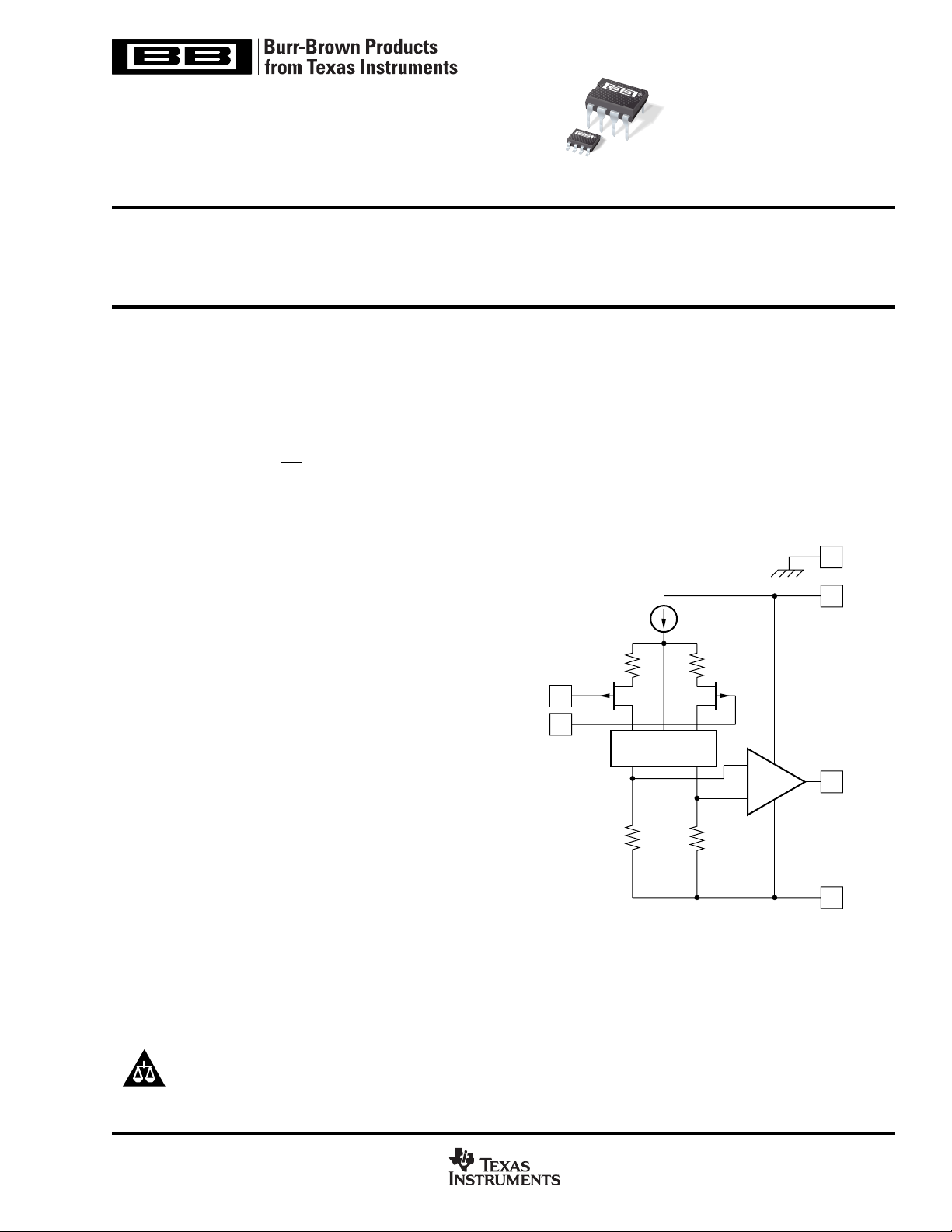
–In
2
3
+In
Noise-Free
Cascode
30kΩ 30kΩ
Simplified Circuit
Substrate
8
7
V+
6
Output
5
V–
Please be aware that an important notice concerning availability, standard warranty, and use in critical applications of
Texas Instruments semiconductor products and disclaimers thereto appears at the end of this data sheet.
Difet is a registered trademark of Texas Instruments.
All other trademarks are the property of their respective owners.
PRODUCTION DATA information is current as of publication date.
Products conform to specifications per the terms of Texas Instruments
standard warranty. Production processing does not necessarily include
testing of all parameters.
Copyright © 1994–2007, Texas Instruments Incorporated
www.ti.com
Page 2
SPECIFICATIONS
ELECTRICAL
At VS = ±15V and TA = +25°C, unless otherwise noted. Pin 8 connected to ground.
OPA129PB, UB OPA129P, U
PARAMETER CONDITION MIN TYP MAX MIN TYP MAX UNITS
INPUT BIAS CURRENT
vs Temperature Doubles every 10°C*
INPUT OFFSET CURRENT V
OFFSET VOLTAGE
Input Offset Voltage VCM = 0V ±0.5 ±2 ±1 ±5mV
vs Temperature ±3 ±10 ±5 µV/°C
Supply Rejection V
NOISE
Voltage f = 10Hz 85 * nV/√Hz
Current f = 10kHz 0.1 * fA/√Hz
INPUT IMPEDANCE
Differential 1013 || 1 * Ω || pF
Common-Mode 10
VOLTAGE RANGE
Common-Mode Input Range ±10 ±12 * * V
Common-Mode Rejection V
OPEN-LOOP GAIN, DC
Open-Loop Voltage Gain RL ≥ 2kΩ 94 120 * * dB
FREQUENCY RESPONSE
Unity Gain, Small Signal 1 * MHz
Full Power Response 20Vp-p, R
Slew Rate V
Settling Time: G = –1, R
0.1% 5*µs
0.01% 10 * µs
Overload Recovery, 50% Overdrive
RATED OUTPUT
Voltage Output RL = 2kΩ±12 ±13 * * V
Current Output V
Load Capacitance Stability Gain = +1 1000 * pF
Short-Circuit Current ±35 ±55 * * mA
POWER SUPPLY
Rated Voltage ±15 * V
Voltage Range, Derated Performance ±5 ±18 * * V
Current, Quiescent I
TEMPERATURE
Specification Ambient Temperature –40 +85 * * °C
Operating Ambient Temperature –40 +125 * * °C
Storage –40 +125 * * °C
Thermal Resistance
DIP-8 90 * °C/W
SO-8 100 * °C/W
NOTES: (1) High-speed automated test.
(2) Overload recovery is defined as the time required for the output to return from saturation to linear operation following the removal of a 50% input
overdrive.
(1)
VCM = 0V ±30 ±100 * ±250 fA
= 0V ±30 * fA
CM
= ±5V to ±18V ±3 ±100 * * µV/V
S
f = 100Hz 28 * nV/√Hz
f = 1kHz 17 * nV/√Hz
f = 10kHz 15 * nV/√Hz
f
= 0.1Hz to 10Hz 4 * µV
B
15
|| 2 * Ω || pF
= ±10V 80 118 * * dB
IN
= 2kΩ 47 * kHz
L
= ±10V, RL = 2kΩ 1 2.5 * * V/µs
O
= 2kΩ, 10V Step
L
(2)
G = –15 *µs
= ±12V ±6 ±10 * * mA
O
= 0mA 1.2 1.8 * * mA
O
θ
, Junction-to-Ambient
JA
PP
2
www.ti.com
OPA129
SBOS026A
Page 3
ABSOLUTE MAXIMUM RATINGS
Power Supply Voltage ......................................................................±18V
Differential Input Voltage ............................................................ V– to V+
Input Voltage Range .................................................................... V– to V+
Storage Temperature Range ......................................... –40°C to +125°C
Operating Temperature Range ......................................–40°C to +125°C
Output Short Circuit Duration
Junction Temperature (T
NOTE: (1) Short circuit may be to power supply common at +25°C ambient.
(1)
..................................................................
) ............................................................ +150°C
J
Continuous
ELECTROSTATIC
DISCHARGE SENSITIVITY
Any integrated circuit can be damaged by ESD. Texas
Instruments recommends that all integrated circuits be
handled with appropriate precautions. Failure to observe proper handling and installation procedures can
cause damage.
ESD damage can range from subtle performance degradation to complete device failure. Precision integrated circuits may be more susceptible to damage
because very small parametric changes could cause
the device not to meet published specifications.
PACKAGE INFORMATION
PRODUCT PACKAGE-LEAD PACKAGE DESIGNATOR
OPA129P DIP-8 P
OPA129PB DIP-8 P
OPA129U SO-8 D
OPA129UB SO-8 D
NOTE: (1) For the most current package and ordering information, see the
Package Option Addendum at the end of this data sheet, or see the TI website
at www.ti.com.
(1)
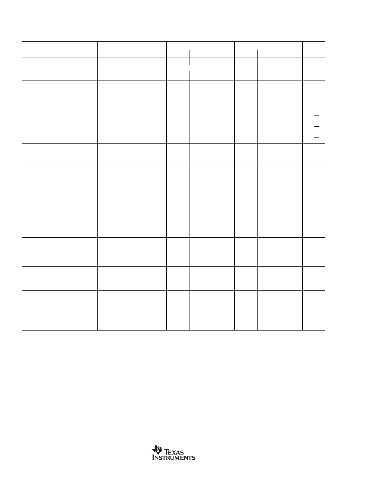
CONNECTION DIAGRAM
Top View DIP/SO
1
NC
2
–In
3
+In
4
NC
NC: No internal connection.
OPA
8
7
6
5
Substrate
V+
Output
V–
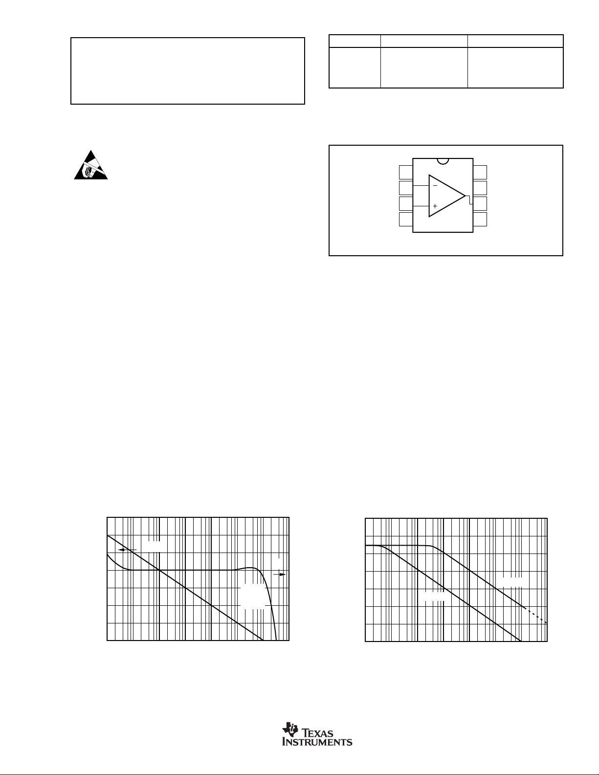
TYPICAL PERFORMANCE CURVES
At TA = +25°C, +15VDC, unless otherwise noted.
140
120
100
80
60
Voltage Gain (dB)
40
20
0
OPA129
SBOS026A
OPEN-LOOP FREQUENCY RESPONSE
Gain
Phase
Margin
≈90°
1001 1M 10M
1k 10k 100k10
Frequency (Hz)
θ
45
90
135
Pulse Shift (degrees)
180
www.ti.com
140
120
100
80
60
40
Power Supply Rejection (dB)
20
POWER SUPPLY REJECTION vs FREQUENCY
0
1001 1M 10M1k 10k 100k10
+PSRR
–PSRR
Frequency (Hz)
3
Page 4
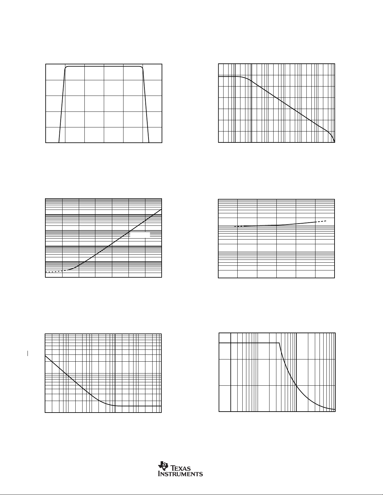
TYPICAL PERFORMANCE CURVES (Cont.)
At TA = +25°C, +15VDC, unless otherwise noted.
COMMON-MODE REJECTION
120
110
100
90
80
Common-Mode Rejection (dB)
70
15 1510 10
100pA
10pA
1pA
vs INPUT COMMON-MODE VOLTAGE
505
Common-Mode Voltage (V)
BIAS AND OFFSET CURRENT vs TEMPERATURE
IB and I
140
120
100
80
60
40
Common-Mode Rejection (dB)
20
10
OS
COMMON-MODE REJECTION vs FREQUENCY
0
1001 1M 10M1k 10k 100k10
Frequency (Hz)
BIAS AND OFFSET CURRENT
vs INPUT COMMON-MODE VOLTAGE
1
100
10
Bias and Offset Current (fA)
1
–50 50 125–25 0 25 75 100
Ambient Temperature (°C)
INPUT VOLTAGE NOISE SPECTRAL DENSITY
1k
100
Voltage Density (nV/√Hz)
10
1 10 100 1k 10k 100k
Frequency (Hz)
0.1
Normalized Bias and Offset Current
0.01
–15 –10 –551015
Common-Mode Voltage (V)
30
)
PP
20
10
Output Voltage (V
0
FULL-POWER OUTPUT vs FREQUENCY
10k 100k1k 1M
0
Frequency (Hz)
4
www.ti.com
OPA129
SBOS026A
Page 5

TYPICAL PERFORMANCE CURVES (Cont.)
At TA = +25°C, +15VDC, unless otherwise noted.
GAIN BANDWIDTH AND SLEW RATE
4
3
2
1
Gain Bandwidth (MHz)
0
–75 125–50 75–25 0 25 50 100
2.0
1.5
1.0
SUPPLY CURRENT vs TEMPERATURE
vs TEMPERATURE
Ambient Temperature (°C)
GAIN BANDWIDTH AND SLEW RATE
4
3
2
Slew Rate (V/µs)
1
0
3
2
1
Gain Bandwidth (MHz)
0
OPEN-LOOP GAIN, PSR AND CMR vs TEMPERATURE
130
120
110
vs SUPPLY VOLTAGE
+Slew
–Slew
GBW
515020
Supply Voltage (±V
10
)
CC
A
OL
CMR
6
4
2
Slew Rate (v/µs)
0
Supply Current (mA)
0.5
0
–75 125–50 75
LARGE SIGNAL TRANSIENT RESPONSE
10
0
Output Voltage (V)
–10
05025
–25 0 25 50 100
Ambient Temperature (°C)
5V
Time (µs)
5µs
100
PSR, CMR, Voltage Gain (dB)
90
–75 125–50 75–25 0 25 50 100
Ambient Temperature (°C)
SMALL SIGNAL TRANSIENT RESPONSE
80
40
0
Output Voltage (mV)
–40
–80
20mV
010
2468
Time (µs)
1µs
PSR
OPA129
SBOS026A
www.ti.com
5
Page 6

TYPICAL PERFORMANCE CURVES (CONT)
TA = +25°C, +15VDC, unless otherwise noted.
COMMON-MODE INPUT RANGE vs SUPPLY VOLTAGE
15
10
5
Common-Mode Voltage (+V)
0
510020
Supply Voltage (±V
15
)
CC
APPLICATIONS INFORMATION
NON-STANDARD PINOUT
The OPA129 uses a non-standard pinout to achieve lowest
possible input bias current. The negative power supply is
connected to pin 5—see Figure 1. This is done to reduce the
leakage current from the V- supply (pin 4 on conventional
op amps) to the op amp input terminals. With this new
pinout, sensitive inputs are separated from both power
supply pins.
R
F
R
V
IN
IN
FIGURE 1. Offset Adjust Circuit.
OFFSET VOLTAGE TRIM
The OPA129 has no conventional offset trim connections.
Pin 1, next to the critical inverting input, has no internal
connection. This eliminates a source of leakage current and
allows guarding of the input terminals. Pin 1 and pin 4, next
to the two input pins, have no internal connection. This
allows an optimized circuit board layout with guarding—see
the Circuit Board Layout section.
V+
2
3
7
OPA129
470kΩ 470kΩ
6
5
V–
V
OUT
V+
0.1µF220Ω
V–
BIAS CURRENT vs ADDITIONAL POWER DISSIPATION
100pA
10pA
1pA
100
Bias Current (fA)
10
1
0 200 35050 100 150 250 300
Additional Power Dissipation (mW)
Due to its laser-trimmed input stage, most applications do
not require external offset voltage trimming. If trimming is
required, the circuit shown in Figure 1 can be used. Power
supply voltages are divided down, filtered and applied to the
non-inverting input. The circuit shown is sensitive to variation in the supply voltages. Regulation can be added, if
needed.
GUARDING AND SHIELDING
Ultra-low input bias current op amps require precautions to
achieve best performance. Leakage current on the surface of
circuit board can exceed the input bias current of the amplifier. For example, a circuit board resistance of 1012Ω from
a power supply pin to an input pin produces a current of
15pA—more than 100 times the input bias current of the op
amp.
To minimize surface leakage, a guard trace should completely surround the input terminals and other circuitry
connecting to the inputs of the op amp. The DIP package
should have a guard trace on both sides of the circuit board.
The guard ring should be driven by a circuit node equal in
potential to the op amp inputs—see Figure 2. The substrate,
pin 8, should also be connected to the circuit board guard to
assure that the amplifier is fully surrounded by the guard
potential. This minimizes leakage current and noise pick-up.
Careful shielding is required to reduce noise pickup. Shielding near feedback components may also help reduce noise
pick-up.
Triboelectric effects (friction-generated charge) can be a
troublesome source of errors. Vibration of the circuit board,
input connectors and input cables can cause noise and drift.
Make the assembly as rigid as possible. Attach cables to
avoid motion and vibration. Special low noise or low leakage cables may help reduce noise and leakage current. Keep
all input connections as short possible. Surface-mount components may reduce circuit board size and allow a more rigid
assembly.
6
www.ti.com
OPA129
SBOS026A
Page 7

CIRCUIT BOARD LAYOUT
2
3
6
8
OPA129
Output
Pin photodiode
HP 5082-4204
5
7
+15V
–15V
0.1µF
5 x 10⁹V/W
0.1µF
1010Ω
~1pF to prevent gain peaking
Guard
Circuit must be well shielded.
2
3
6
7
5
8
OPA129
1000MΩ
R
F
Output
V
O
= –IIN • R
F
VO = –10V/nA
18kΩ
2kΩ
Current
Input
I
IN
V–
V+
The OPA129 uses a new pinout for ultra low input bias
current. Pin 1 and pin 4 have no internal connection. This
allows ample circuit board space for a guard ring surrounding the op amp input pins—even with the tiny SO-8 surfacemount package. Figure 3 shows suggested circuit board
layouts. The guard ring should be connected to pin 8 (substrate) as shown. It should be driven by a circuit node equal
in potential to the input terminals of the op amp—see Figure
2 for common circuit configurations.
TESTING
Accurately testing the OPA129 is extremely difficult due to
its high performance. Ordinary test equipment may not be
able to resolve the amplifier’s extremely low bias current.
Inaccurate bias current measurements can be due to:
1. Test socket leakage.
2. Unclean package.
3. Humidity or dew point condensations.
4. Circuit contamination from fingerprints or anti-static
treatment chemicals.
5. Test ambient temperature.
6. Load power dissipation.
7. Mechanical stress.
8. Electrostatic and electromagnetic interference.
(A) Non-Inverting
2
3
In
8
Out
6
In
(C) Inverting
In
2
3
8
(B) Buffer
2
3
Out
6
8
6
Out
FIGURE 4. Current-to-Voltage Converter.
500Ω 9.5kΩ
2
OPA129
3
V+
8
7
6
5
V–
Output
pH Probe
R
≈ 500MΩ
S
50mV Out
Guard
FIGURE 5. High Impedance (1015Ω) Amplifier.
C
10pF
F
11
Ω
10
R
F
V+
8
2
∆Q
OPA129
3
7
5
Low frequency cutoff =
V–
1/(2πR
V
OUT
6
= –∆Q/C
) = 0.16Hz
FCF
Output
1VDC
V
OUT
F
Guard top and bottom of board.
FIGURE 2. Connection of Input Guard.
18
4
(A) DIP package
FIGURE 3. Suggested Board Layout for Input Guard.
OPA129
SBOS026A
(B) SOIC package
5
18
4
5
Connect to proper circuit
node, depending on circuit
V+
configuration (see Figure 2).
V
0
V–
Connect to proper circuit
node, depending on circuit
V+
configuration (see Figure 2).
V
0
V–
FIGURE 6. Piezoelectric Transducer Charge Amplifier.
FIGURE 7. Sensitive Photodiode Amplifier.
www.ti.com
7
Page 8

PACKAGE OPTION ADDENDUM
www.ti.com
24-Feb-2009
PACKAGING INFORMATION
Orderable Device Status
(1)
Package
Type
Package
Drawing
Pins Package
Qty
Eco Plan
OPA129P OBSOLETE PDIP P 8 TBD Call TI Call TI
OPA129PB OBSOLETE PDIP P 8 TBD Call TI CallTI
OPA129U ACTIVE SOIC D 8 75 Green (RoHS &
no Sb/Br)
OPA129UB ACTIVE SOIC D 8 75 Green (RoHS &
no Sb/Br)
OPA129UB/2K5 ACTIVE SOIC D 8 2500 Green (RoHS &
no Sb/Br)
OPA129UB/2K5E4 ACTIVE SOIC D 8 2500 Green (RoHS &
no Sb/Br)
OPA129UBE4 ACTIVE SOIC D 8 75 Green (RoHS &
no Sb/Br)
OPA129UBG4 ACTIVE SOIC D 8 75 Green (RoHS &
no Sb/Br)
OPA129UE4 ACTIVE SOIC D 8 75 Green (RoHS &
no Sb/Br)
(1)
The marketing status values are defined as follows:
ACTIVE: Product device recommended for new designs.
LIFEBUY: TI has announced that the device will be discontinued, and a lifetime-buy period is in effect.
NRND: Not recommended for new designs. Device is in production to support existing customers, but TI does not recommend using this part in
a new design.
PREVIEW: Device has been announced but is not in production. Samples may or may not be available.
OBSOLETE: TI has discontinued the production of the device.
(2)
Lead/Ball Finish MSL Peak Temp
CU NIPDAU Level-3-260C-168 HR
CU NIPDAU Level-3-260C-168 HR
CU NIPDAU Level-3-260C-168 HR
CU NIPDAU Level-3-260C-168 HR
CU NIPDAU Level-3-260C-168 HR
CU NIPDAU Level-3-260C-168 HR
CU NIPDAU Level-3-260C-168 HR
(3)
(2)
Eco Plan - The planned eco-friendly classification: Pb-Free (RoHS), Pb-Free (RoHS Exempt), or Green (RoHS & no Sb/Br) - please check
http://www.ti.com/productcontent for the latest availability information and additional product content details.
TBD: The Pb-Free/Green conversion plan has not been defined.
Pb-Free (RoHS): TI's terms "Lead-Free" or "Pb-Free" mean semiconductor products that are compatible with the current RoHS requirements
for all 6 substances, including the requirement that lead not exceed 0.1% by weight in homogeneous materials. Where designed to be soldered
at high temperatures, TI Pb-Free products are suitable for use in specified lead-free processes.
Pb-Free (RoHS Exempt): This component has a RoHS exemption for either 1) lead-based flip-chip solder bumps used between the die and
package, or 2) lead-based die adhesive used between the die and leadframe. The component is otherwise considered Pb-Free (RoHS
compatible) as defined above.
Green (RoHS & no Sb/Br): TI defines "Green" to mean Pb-Free (RoHS compatible), and free of Bromine (Br) and Antimony (Sb) based flame
retardants (Br or Sb do not exceed 0.1% by weight in homogeneous material)
(3)
MSL, Peak Temp. -- The Moisture Sensitivity Level rating according to the JEDEC industry standard classifications, and peak solder
temperature.
Important Information and Disclaimer:The information provided on this page represents TI's knowledge and belief as of the date that it is
provided. TI bases its knowledge and belief on information provided by third parties, and makes no representation or warranty as to the
accuracy of such information. Efforts are underway to better integrate information from third parties. TI has taken and continues to take
reasonable steps to provide representative and accurate information but may not have conducted destructive testing or chemical analysis on
incoming materials and chemicals. TI and TI suppliers consider certain information to be proprietary, and thus CAS numbers and other limited
information may not be available for release.
In no event shall TI's liability arising out of such information exceed the total purchase price of the TI part(s) at issue in this document sold by TI
to Customer on an annual basis.
Addendum-Page 1
Page 9

PACKAGE MATERIALS INFORMATION
www.ti.com 14-Jul-2009
TAPE AND REEL INFORMATION
*All dimensions arenominal
Device Package
OPA129UB/2K5 SOIC D 8 2500 330.0 12.4 6.4 5.2 2.1 8.0 12.0 Q1
Type
Package
Drawing
Pins SPQ Reel
Diameter
(mm)
Reel
Width
W1 (mm)
A0 (mm) B0 (mm) K0 (mm) P1
(mm)W(mm)
Pin1
Quadrant
Pack Materials-Page 1
Page 10

PACKAGE MATERIALS INFORMATION
www.ti.com 14-Jul-2009
*All dimensions arenominal
Device Package Type Package Drawing Pins SPQ Length (mm) Width (mm) Height (mm)
OPA129UB/2K5 SOIC D 8 2500 346.0 346.0 29.0
Pack Materials-Page 2
Page 11

Page 12

MECHANICAL DATA
MPDI001A – JANUARY 1995 – REVISED JUNE 1999
P (R-PDIP-T8) PLASTIC DUAL-IN-LINE
0.400 (10,60)
0.355 (9,02)
8
5
0.260 (6,60)
0.240 (6,10)
1
0.021 (0,53)
0.015 (0,38)
NOTES: A. All linear dimensions are in inches (millimeters).
B. This drawing is subject to change without notice.
C. Falls within JEDEC MS-001
4
0.070 (1,78) MAX
0.020 (0,51) MIN
0.200 (5,08) MAX
0.125 (3,18) MIN
0.100 (2,54)
0.010 (0,25)
Seating Plane
M
0.325 (8,26)
0.300 (7,62)
0.015 (0,38)
Gage Plane
0.010 (0,25) NOM
0.430 (10,92)
MAX
4040082/D 05/98
For the latest package information, go to http://www.ti.com/sc/docs/package/pkg_info.htm
POST OFFICE BOX 655303 • DALLAS, TEXAS 75265
Page 13

IMPORTANT NOTICE
Texas Instruments Incorporated and its subsidiaries (TI) reserve the right to make corrections, modifications, enhancements, improvements,
and other changes to its products and services at any time and to discontinue any product or service without notice. Customers should
obtain the latest relevant information before placing orders and should verify that such information is current and complete. All products are
sold subject to TI’s terms and conditions of sale supplied at the time of order acknowledgment.
TI warrants performance of its hardware products to the specifications applicable at the time of sale in accordance with TI’s standard
warranty. Testing and other quality control techniques are used to the extent TI deems necessary to support this warranty. Except where
mandated by government requirements, testing of all parameters of each product is not necessarily performed.
TI assumes no liability for applications assistance or customer product design. Customers are responsible for their products and
applications using TI components. To minimize the risks associated with customer products and applications, customers should provide
adequate design and operating safeguards.
TI does not warrant or represent that any license, either express or implied, is granted under any TI patent right, copyright, mask work right,
or other TI intellectual property right relating to any combination, machine, or process in which TI products or services are used. Information
published by TI regarding third-party products or services does not constitute a license from TI to use such products or services or a
warranty or endorsement thereof. Use of such information may require a license from a third party under the patents or other intellectual
property of the third party, or a license from TI under the patents or other intellectual property of TI.
Reproduction of TI information in TI data books or data sheets is permissible only if reproduction is without alteration and is accompanied
by all associated warranties, conditions, limitations, and notices. Reproduction of this information with alteration is an unfair and deceptive
business practice. TI is not responsible or liable for such altered documentation. Information of third parties may be subject to additional
restrictions.
Resale of TI products or services with statements different from or beyond the parameters stated by TI for that product or service voids all
express and any implied warranties for the associated TI product or service and is an unfair and deceptive business practice. TI is not
responsible or liable for any such statements.
TI products are not authorized for use in safety-critical applications (such as life support) where a failure of the TI product would reasonably
be expected to cause severe personal injury or death, unless officers of the parties have executed an agreement specifically governing
such use. Buyers represent that they have all necessary expertise in the safety and regulatory ramifications of their applications, and
acknowledge and agree that they are solely responsible for all legal, regulatory and safety-related requirements concerning their products
and any use of TI products in such safety-critical applications, notwithstanding any applications-related information or support that may be
provided by TI. Further, Buyers must fully indemnify TI and its representatives against any damages arising out of the use of TI products in
such safety-critical applications.
TI products are neither designed nor intended for use in military/aerospace applications or environments unless the TI products are
specifically designated by TI as military-grade or "enhanced plastic." Only products designated by TI as military-grade meet military
specifications. Buyers acknowledge and agree that any such use of TI products which TI has not designated as military-grade is solely at
the Buyer's risk, and that they are solely responsible for compliance with all legal and regulatory requirements in connection with such use.
TI products are neither designed nor intended for use in automotive applications or environments unless the specific TI products are
designated by TI as compliant with ISO/TS 16949 requirements. Buyers acknowledge and agree that, if they use any non-designated
products in automotive applications, TI will not be responsible for any failure to meet such requirements.
Following are URLs where you can obtain information on other Texas Instruments products and application solutions:
Products Applications
Amplifiers amplifier.ti.com Audio www.ti.com/audio
Data Converters dataconverter.ti.com Automotive www.ti.com/automotive
DLP® Products www.dlp.com Broadband www.ti.com/broadband
DSP dsp.ti.com Digital Control www.ti.com/digitalcontrol
Clocks and Timers www.ti.com/clocks Medical www.ti.com/medical
Interface interface.ti.com Military www.ti.com/military
Logic logic.ti.com Optical Networking www.ti.com/opticalnetwork
Power Mgmt power.ti.com Security www.ti.com/security
Microcontrollers microcontroller.ti.com Telephony www.ti.com/telephony
RFID www.ti-rfid.com Video & Imaging www.ti.com/video
RF/IF and ZigBee® Solutions www.ti.com/lprf Wireless www.ti.com/wireless
Mailing Address: Texas Instruments, Post Office Box 655303, Dallas, Texas 75265
Copyright © 2009, Texas Instruments Incorporated
 Loading...