

VIOmax
STABLE
25 µV
25°C to 85°C
100 µV
25 µV
55°C to 125°C
100 µV
查询OP27A供应商
OP27A, OP27C, OP27E, OP27G
OP37A, OP37C, OP37E, OP37G
LOW-NOISE HIGH-SPEED PRECISION OPERATIONAL AMPLIFIERS
SLOS100B – FEBRUARY 1989 – REVISED AUGUST 1994
• Direct Replacements for PMI and LTC OP27
and OP37 Series
Features of OP27A, OP27C, OP37A, and
OP37C:
• Maximum Equivalent Input Noise Voltage:
3.8 nV/√Hz
5.5 nV/√Hz
at 1 kHz
at 10 kHz
• Very Low Peak-to-Peak Noise Voltage at
0.1 Hz to 10 Hz . . . 80 nV Typ
• Low Input Offset Voltage ...25 µV Max
• High Voltage Amplification ...1 V/µV Min
Feature of OP37 Series:
• Minimum Slew Rate ...11 V/µs
description
The OP27 and OP37 operational amplifiers
combine outstanding noise performance with
excellent precision and high-speed specifications.
The wideband noise is only 3 nV/√Hz
1/f noise corner at 2.7 Hz, low noise is maintained
for all low-frequency applications.
The outstanding characteristics of the OP27 and
OP37 make these devices excellent choices
for low-noise amplifier applications requiring
precision performance and reliability . Additionally ,
the OP37 is free of latch-up in high-gain,
large-capacitive-feedback configurations.
The OP27 series is compensated for unity gain.
The OP37 series is decompensated for increased
bandwidth and slew rate and is stable down to a
gain of 5.
The OP27A, OP27C, OP37A, and OP37C are
characterized for operation over the full military
temperature range of –55°C to 125°C. The
OP27E, OP27G, OP37E, and OP37G are
characterized for operation from – 25°C to 85°C.
T
A
°
–
°
–
°
°
AT 25°C
and with the
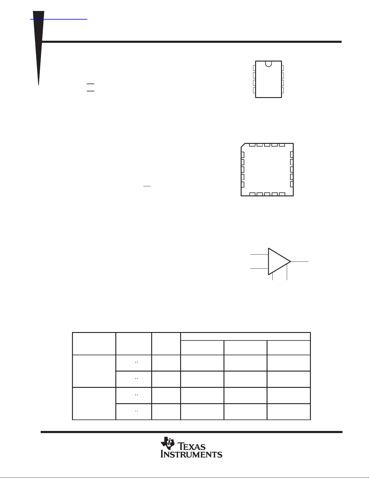
JG OR P PACKAGE
(TOP VIEW)
VIO TRIM
V
CC –
NC
1N–
NC
IN+
NC
NC – No internal connection
1
IN–
2
IN +
3
4
FK PACKAGE
(TOP VIEW)
NC
V TRIM
3 2 1 20 19
4
5
6
7
8
910111213
NC
V
IO
NCNCNC
NC
CC –
8
7
6
5
NC
IO
V TRIM
symbol
3
2
+
–
18
VIO TRIM
PLASTIC DIP
IN+
IN –
Pin numbers are for the JG and P packages.
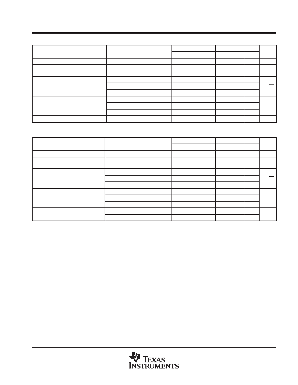
AVAILABLE OPTIONS
PACKAGE
GAIN
1 — — OP27EP
5 — — OP37EP
1 — — OP27GP
5 — — OP37GP
1 OP27AJG OP27AFK —
5 OP37AJG OP37AFK —
1 OP27CJG — —
5 OP37CJG — —
CERAMIC DIP
(JG)
CHIP CARRIER
(FK)
VIO TRIM
V
CC+
OUT
NC
NC
18
V
17
CC+
NC
16
OUT
15
NC
14
(P)
6
OUT
PRODUCTION DATA information is current as of publication date.
Products conform to specifications per the terms of Texas Instruments
standard warranty. Production processing does not necessarily include
testing of all parameters.
POST OFFICE BOX 655303 • DALLAS, TEXAS 75265
POST OFFICE BOX 1443
• HOUSTON, TEXAS 77251–1443
Copyright 1994, Texas Instruments Incorporated
2–1
OP27A, OP27C, OP27E, OP27G
OP37A, OP37C, OP37E, OP37G
LOW-NOISE HIGH-SPEED OPERATIONAL AMPLIFIER
SLOS100B – FEBRUARY 1989 – REVISED AUGUST 1994
V
+
CC
260
750
480 µA
–
OUT
Q46
µA
Q19
Q20
µA
†
C1
Q22
Q24Q23
Q45
340
Q26
CC
V
µA
TRIM
IO
TRIM V
IO
V
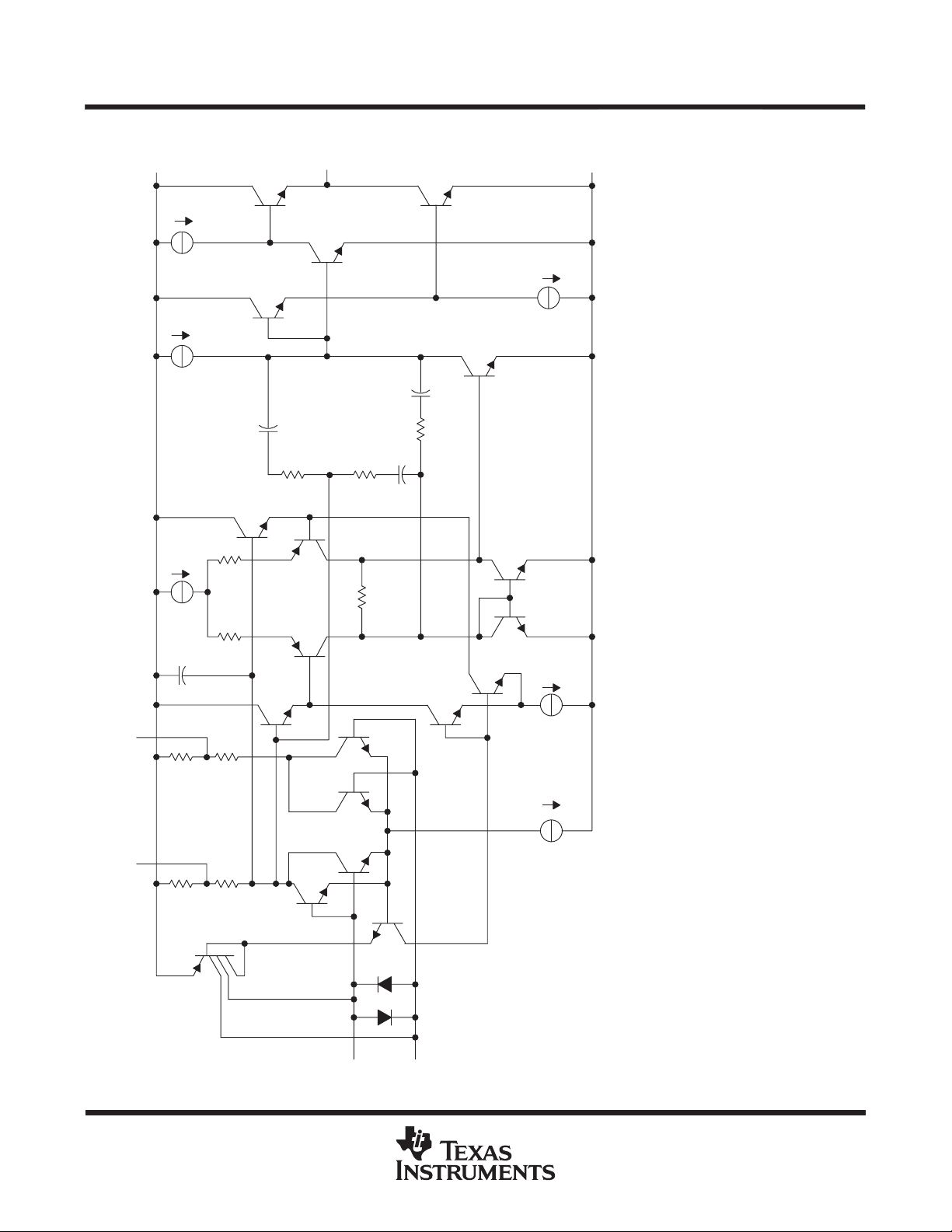
schematic
Q6
Q21
Q1A
Q1B Q2B Q2A
IN +
Q3
IN –
Q27 Q28
Q12
Q11
240 µA 120
µA
C1 = 120 pF for OP27
C1 = 15 pF for OP37
†
2–2
POST OFFICE BOX 655303 DALLAS, TEXAS 75265POST OFFICE BOX 1443 HOUSTON, TEXAS 77251–1443
••

OP27A, OP27C, OP27E, OP27G
OP37A, OP37C, OP37E, OP37G
LOW-NOISE HIGH-SPEED PRECISION OPERATIONAL AMPLIFIERS
SLOS100B – FEBRUARY 1989 – REVISED AUGUST 1994
absolute maximum ratings over operating free-air temperature range (unless otherwise noted)
Supply voltage, V
Supply voltage, V
Input voltage, V
(see Note 1) 22 V. . . . . . . . . . . . . . . . . . . . . . . . . . . . . . . . . . . . . . . . . . . . . . . . . . . . . . . . . .
CC+
(see Note 1) – 22 V. . . . . . . . . . . . . . . . . . . . . . . . . . . . . . . . . . . . . . . . . . . . . . . . . . . . . . . . .
CC–
V
. . . . . . . . . . . . . . . . . . . . . . . . . . . . . . . . . . . . . . . . . . . . . . . . . . . . . . . . . . . . . . . . . . . . . . . . .
I
Duration of output short circuit unlimited. . . . . . . . . . . . . . . . . . . . . . . . . . . . . . . . . . . . . . . . . . . . . . . . . . . . . . . . . . .
Differential input current (see Note 2) ±25 mA. . . . . . . . . . . . . . . . . . . . . . . . . . . . . . . . . . . . . . . . . . . . . . . . . . . . .
Continuous power dissipation See Dissipation Rating Table. . . . . . . . . . . . . . . . . . . . . . . . . . . . . . . . . . . . . . . . .
Operating free-air temperature range: OP27A, OP27C, OP37A, OP37C – 55°C to 125°C. . . . . . . . . . . . . . .
OP27E, OP27G, OP37E, OP37G – 25°C to 85°C. . . . . . . . . . . . . . .
Storage temperature range – 65°C to 150°C. . . . . . . . . . . . . . . . . . . . . . . . . . . . . . . . . . . . . . . . . . . . . . . . . . . . . . .
Lead temperature 1,6 mm (1/16 inch) from case for 60 seconds: JG or FK package 300°C. . . . . . . . . . . . . .
Lead temperature 1,6 mm (1/16 inch) from case for 10 seconds : P package 260°C. . . . . . . . . . . . . . . . . . . .
NOTES: 1. All voltage values are with respect to the midpoint between V
2. The inputs are protected by back-to-back diodes. Current-limiting resistors are not used in order to achieve low noise. Excessive
input current will flow if a differential input voltage in excess of approximately ± 0.7 V is applied between the inputs unless some
limiting resistance is used.
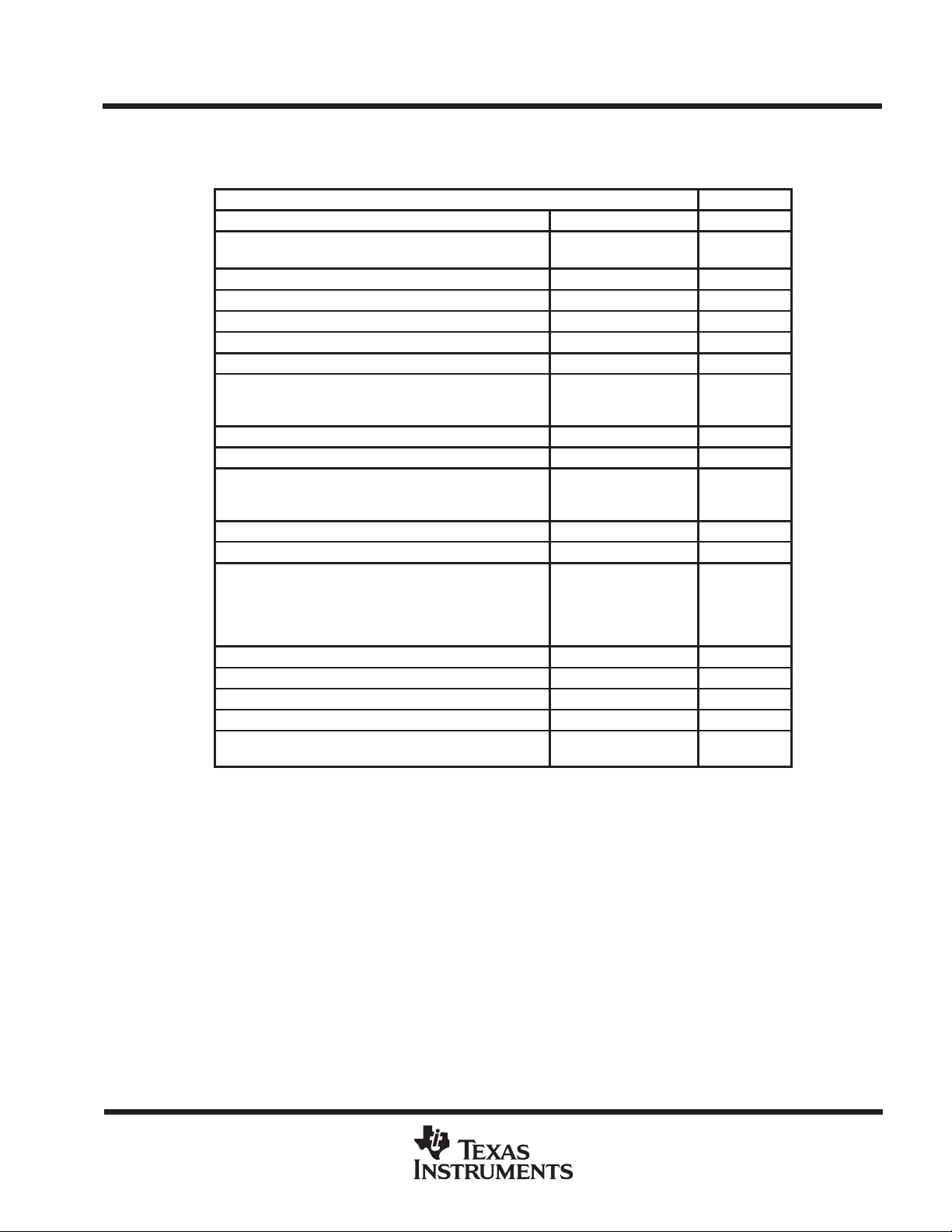
DISSIPATION RATING TABLE
PACKAGE
JG
FK
P
TA ≤ 25°C
POWER RATING
1050 mW
1375 mW
1000 mW
DERATING FACTOR
ABOVE TA = 25°C
8.4 mW/°C
11.0 mW/°C
8.0 mW/°C
CC+
and V
unless otherwise noted.
CC–
TA = 85°C
POWER RATING
546 mW
715 mW
520 mW
TA = 125°C
POWER RATING
210 mW
275 mW
N/A
CC±
POST OFFICE BOX 655303 • DALLAS, TEXAS 75265
POST OFFICE BOX 1443
• HOUSTON, TEXAS 77251–1443
2–3
OP27A, OP27C, OP27E, OP27G
UNIT
Common-mode input voltage, V
V
PARAMETER
TEST CONDITIONS
T
†
UNIT
VIOInput offset voltage
O
,
IC
V
IIOInput offset current
V
V
0
nA
IIBInput bias current
V
V
0
nA
V
V
Large-signal differential
CMRR
j
dB
k
ygj
dB
OP37A, OP37C, OP37E, OP37G
LOW-NOISE HIGH-SPEED PRECISION OPERATIONAL AMPLIFIERS
SLOS100B – FEBRUARY 1989 – REVISED AUGUST 1994
recommended operating conditions
OP27A, OP37A OP27C, OP37C
MIN NOM MAX MIN NOM MAX
Supply voltage, V
Supply voltage, V
Operating free-air temperature, T
CC+
CC–
p
V
= ± 15 V, TA = 25°C ± 11 ±11
IC
CC±
V
= ± 15 V, TA = – 55°C to 125°C ±10.3 ±10.2
CC±
A
4 15 22 4 15 22 V
–4 –15 –22 –4 –15 –22 V
–55 125 –55 125 °C
electrical characteristics at specified free-air temperature, V
A
V
p
Average temperature
α
V
A
r
i(CM)
r
o
†
Full range is – 55°C to 125°C.
NOTES: 3. Input offset voltage measurements are performed by automatic test equipment approximately 0.5 seconds after applying power.
coefficient of input
VIO
offset voltage
Long-term drift of input
offset voltage
p
p
Common-mode input
ICR
voltage range
Peak output voltage swing
OM
VD
voltage amplification
Common-mode input
resistance
Output resistance VO = 0, IO = 0 25°C 70 70 Ω
Common-mode rejection
ratio
Supply voltage rejection
SVR
ratio
4. Long-term drift of input offset voltage refers to the average trend line of offset voltage versus time over extended periods after the
first 30 days of operation. Excluding the initial hour of operation, changes in VIO during the first 30 days are typically 2.5 µV
(see Figure 3).
= 0, V
RS = 50 Ω, See Note 3
See Note 4 0.2 1 0.4 2 µV/mo
= 0,
O
= 0,
O
RL ≥ 2 kΩ ±12 ±13.8 ±11.5 ±13.5
RL ≥ 0.6 kΩ
RL ≥ 2 kΩ Full range ±11.5 10.5
RL ≥ 2 kΩ, VO = ±10 V 1000 1800 700 1500
RL ≥ 1 kΩ, VO = ±10 V 800 1500 1500
RL ≥ 0.6 kΩ, VO = ±1 V,
V
= ± 4 V
CC±
RL ≥ 2 kΩ, VO = ±10 V Full range 600 300
VIC = ±11 V 25°C 114 126 100 120
VIC = ±10 V
V
= ±4 V to ±18 V 25°C 100 120 94 118
CC±
V
= ±4.5 V to ±18 V Full range 96 86
CC±
= 0
=
IC
=
IC
25°C 10 25 30 100
Full range 60 300
Full range 0.2 0.6 0.4 1.8 µV/°C
25°C 7 35 12 75
Full range 50 135
25°C ±10 ±40 ±15 ±80
Full range ±60 ±150
25°C
Full range
Full range 110 94
MIN TYP MAX MIN TYP MAX
–11
10.3
–10.3
±10 ±11.5 ±10 ±1 1.5
250 700 200 500
= ±15 V (unless otherwise noted)
CC±
OP27A, OP37A OP27C, OP37C
11
to
to
3 2 GΩ
11
to
–11
10.5
to
–10.5
µ
V
V/mV
2–4
POST OFFICE BOX 655303 • DALLAS, TEXAS 75265
POST OFFICE BOX 1443
• HOUSTON, TEXAS 77251–1443
LOW-NOISE HIGH-SPEED PRECISION OPERATIONAL AMPLIFIERS
Common-mode input voltage, V
V
PARAMETER
TEST CONDITIONS
T
†
UNIT
VIOInput offset voltage
O
,
IC
V
IIOInput offset current
V
V
0
nA
IIBInput bias current
V
0
V
0
nA
V
V
Large-signal differential
CMRR
j
dB
k
ygj
dB
recommended operating conditions
Supply voltage, V
Supply voltage, V
Operating free-air temperature, T
CC+
CC –
p
IC
A
OP27A, OP27C, OP27E, OP27G
OP37A, OP37C, OP37E, OP37G
SLOS100B – FEBRUARY 1989 – REVISED AUGUST 1994
V
= ±15 V, TA = 25°C ±11
CC±
V
= ±15 V, TA = – 55°C to 125°C ±10.5
CC±
MIN NOM MAX UNIT
4 15 22 V
–4 –15 –22 V
–25 85 °C
electrical characteristics at specified free-air temperature, V
A
V
p
Average temperature
αV
V
A
r
i(CM)
r
o
†
Full range is – 25°C to 85°C.
NOTES: 3. Input offset voltage measurements are performed by automatic test equipment approximately 0.5 seconds after applying power .
coefficient of input
IO
offset voltage
Long-term drift of input
offset voltage
p
p
Common-mode input
ICR
voltage range
Peak output voltage swing
OM
VD
voltage amplification
Common-mode input
resistance
Output resistance VO = 0, IO = 0 25°C 70 70 Ω
Common-mode rejection
ratio
Supply voltage rejection
SVR
ratio
4. Long-term drift of input offset voltage refers to the average trend line of offset voltage versus time over extended periods after the
first 30 days of operation. Excluding the initial hour of operation, changes in VIO during the first 30 days are typically 2.5 µV
(see Figure 3).
= 0, V
RS = 50 Ω, See Note 3
See Note 4 0.2 1 0.4 2 µV/mo
= 0,
O
,
=
O
RL ≥ 2 kΩ ±12 ±13.8 ±11.5 ±13.5
RL ≥ 0.6 kΩ
RL ≥ 2 kΩ Full range ±1 1.5 10.5
RL ≥ 2 kΩ, VO = ±10 V 1000 1800 700 1500
RL ≥ 1 kΩ, VO = ±10 V 800 1500 1500
RL ≥ 0.6 kΩ, VO = ±1 V,
V
= ± 4 V
CC±
RL ≥ 2 kΩ, VO = ± 10 V Full range 600 450
VIC = ±11 V 25°C 114 126 100 120
VIC = ±10 V
V
= ± 4 V to ±18 V 25°C 100 120 94 118
CC±
V
= ± 4.5 V to ±18 V Full range 96 90
CC±
= 0
=
IC
=
IC
25°C 10 25 30 100
Full range 60 220
Full range 0.2 0.6 0.4 1.8 µV/°C
25°C 7 35 12 75
Full range 50 135
25°C ±10 ±40 ±15 ±80
Full range ±60 ±150
25°C
Full range
Full range 110 96
MIN TYP MAX MIN TYP MAX
–11
10.3
–10.3
±10 ±11.5 ±10 ±1 1.5
250 700 200 500
= ±15 V (unless otherwise noted)
±
CC
OP27E, OP37E OP27G, OP37G
11
to
to
3 2 GΩ
11
to
–11
10.5
to
–10.5
µ
V
V/mV
POST OFFICE BOX 655303 • DALLAS, TEXAS 75265
POST OFFICE BOX 1443
• HOUSTON, TEXAS 77251–1443
2–5
OP27A, OP27C, OP27E, OP27G
PARAMETER
TEST CONDITIONS
UNIT
PARAMETER
TEST CONDITIONS
UNIT
voltage
Gain-bandwidth product
MH
OP37A, OP37C, OP37E, OP37G
LOW-NOISE HIGH-SPEED PRECISION OPERATIONAL AMPLIFIERS
SLOS100B – FEBRUARY 1989 – REVISED AUGUST 1994
OP27 operating characteristics over operating free-air temperature range, V
OP27A, OP27E OP27C, OP27G
MIN TYP MAX MIN TYP MAX
SR Slew rate AVD ≥ 1, RL ≥ 2 kΩ 1.7 2.8 1.7 2.8 V/µs
V
N(PP)
V
n
I
n
Peak-to-peak equivalent
input noise voltage
Equivalent input noise voltage
Equivalent input noise current
Gain-bandwidth product f = 100 kHz 5 8 5 8 MHz
f = 0.1 Hz to 10 Hz, RS = 20 Ω,
See Figure 34
f = 10 Hz, RS = 20 Ω 3.5 5.5 3.8 8
f = 30 Hz, RS = 20 Ω
f = 1 kHz, RS = 20 Ω 3 3.8 3.2 4.5
f = 10 Hz, See Figure 35 1.5 4 1.5
f = 30 Hz, See Figure 35
f = 1 kHz, See Figure 35 0.4 0.6 0.4 0.6
0.08 0.18 0.09 0.25 µV
3.1 4.5 3.3 5.6
1 2.3 1
OP37 operating characteristics over operating free-air temperature range, V
OP37A, OP37E OP37C, OP37G
MIN TYP MAX MIN TYP MAX
SR Slew rate AVD ≥ 5, RL ≥ 2 kΩ 11 17 11 17 V/µs
V
N(PP)
V
n
I
n
Peak-to-peak equivalent
input noise voltage
Equivalent input noise
Equivalent input noise current
p
f = 0.1 Hz to 10 Hz, RS = 20 Ω,
See Figure 34
f = 10 Hz, RS = 20 Ω 3.5 5.5 3.8 8
f = 30 Hz, RS = 20 Ω 3.1 4.5 3.3 5.6
f = 1 kHz, RS = 20 Ω 3 3.8 3.2 4.5
f = 10 Hz, See Figure 35 1.5 4 1.5
f = 30 Hz, See Figure 35
f = 1 kHz, See Figure 35 0.4 0.6 0.4 0.6
f = 10 kHz 45 63 45 63
AV ≥ 5, f = 1 MHz 40 40
0.08 0.18 0.09 0.25 µV
1 2.3 1
CC±
CC±
= ±15 V
= ±15 V
nV/√Hz
pA/√Hz
nV/√Hz
pA/√Hz
z
2–6
POST OFFICE BOX 655303 • DALLAS, TEXAS 75265
POST OFFICE BOX 1443
• HOUSTON, TEXAS 77251–1443
OP27A, OP27C, OP27E, OP27G
OP37A, OP37C, OP37E, OP37G
LOW-NOISE HIGH-SPEED PRECISION OPERATIONAL AMPLIFIERS
SLOS100B – FEBRUARY 1989 – REVISED AUGUST 1994
TYPICAL CHARACTERISTICS
Table of Graphs
FIGURE
V
IO
∆V
I
IO
I
IB
V
ICR
V
OM
V
O(PP)
A
VD
CMRR Common-mode rejection ratio vs Frequency 15
k
SVR
SR Slew rate
φ
m
φ Phase shift vs Frequency 12, 13
V
n
I
n
I
OS
I
CC
Input offset voltage vs Temperature 1
Change in input offset voltage
IO
Input offset current vs Temperature 4
Input bias current vs Temperature 5
Common-mode input voltage range vs Supply voltage 6
Maximum peak output voltage vs Load resistance 7
Maximum peak-to-peak output voltage vs Frequency 8, 9
Differential voltage amplification
Supply voltage rejection ratio vs Frequency 16
Phase margin vs Temperature 20, 21
Equivalent input noise voltage
Equivalent input noise current vs Frequency 27
Gain-bandwidth product vs Temperature 20, 21
Short-circuit output current vs Time 28
Supply current vs Supply voltage 29
Pulse response
vs Time after power on
vs Time (long-term drift)
vs Supply voltage
vs Load resistance
vs Frequency
vs Temperature
vs Supply voltage
vs Load resistance
vs Bandwidth
vs Source resistance
vs Supply voltage
vs Temperature
vs Frequency
Small signal
Large signal
2
3
10
11
12, 13, 14
17
18
19
22
23
24
25
26
30, 32
31, 33
POST OFFICE BOX 655303 • DALLAS, TEXAS 75265
POST OFFICE BOX 1443
• HOUSTON, TEXAS 77251–1443
2–7

OP27A, OP27C, OP27E, OP27G
OP37A, OP37C, OP37E, OP37G
LOW-NOISE HIGH-SPEED PRECISION OPERATIONAL AMPLIFIERS
SLOS100B – FEBRUARY 1989 – REVISED AUGUST 1994
TYPICAL CHARACTERISTICS
INPUT OFFSET VOLTAGE OF
REPRESENTATIVE INDIVIDUAL UNITS
vs
FREE-AIR TEMPERATURE
100
V
= ±15 V
80
60
µV
40
20
0
– 20
– 40
– Input Offset Voltage – V
IO
– 60
– 80
– 100
– 50 – 25 0 25 50 75 100 125
CC±
OP27C/37C
OP27A/37A
OP27E/37E
OP27G/37G
OP27C/37C
TA – Free-Air T emperature – °C
OP27A/37A
†
WARM-UP CHANGE IN
INPUT OFFSET VOLTAGE
vs
ELAPSED TIME
V
= ±15 V
CC±
TA = 25°C
10
OP27CP/GP
OP37CP/GP
5
OP27AP/EP
– Change in Input Offset Voltage – Vµ
IO
∆V
0
12345
Time After Power On – minutes
OP37AP/EP
Figure 1 Figure 2
LONG-TERM DRIFT OF INPUT OFFSET VOLTAGE OF
REPRESENTATIVE INDIVIDUAL UNITS
6
0.2-µV/mo Trend Line
4
2
0
– 2
– Change in Input Offset Voltage – Vµ
– 4
IO
∆V
0.2-µV/mo Trend Line
– 6
012345678
Time – months
Figure 3
†
Data for temperatures below – 25°C and above 85°C are applicable to the OP27A, OP27C, OP37A, and OP37C only.
2–8
POST OFFICE BOX 655303 • DALLAS, TEXAS 75265
POST OFFICE BOX 1443
• HOUSTON, TEXAS 77251–1443

OP27A, OP27C, OP27E, OP27G
OP37A, OP37C, OP37E, OP37G
LOW-NOISE HIGH-SPEED PRECISION OPERATIONAL AMPLIFIERS
SLOS100B – FEBRUARY 1989 – REVISED AUGUST 1994
INPUT OFFSET CURRENT
FREE-AIR TEMPERATURE
50
V
= ±15 V
CC±
40
30
20
– Input Offset Current – nA
IO
I
10
OP27A/E
OP37A/E
0
– 75 – 50 – 25 0 50 75 100 12525
TA – Free-Air Temperature – ° C
TYPICAL CHARACTERISTICS
vs
OP27C/G
OP37C/G
†
INPUT BIAS CURRENT
FREE-AIR TEMPERATURE
± 50
V
= ±15 V
CC±
± 40
± 30
± 20
– Input Bias Current – nA
IB
I
± 10
OP27A/E
OP37A/E
0
– 50 – 25 0 50 75 100 12525
– 75
TA – Free-Air Temperature – ° C
vs
OP27C/G
OP37C/G
Figure 4 Figure 5
COMMON-MODE INPUT VOLTAGE RANGE LIMITS
vs
SUPPLY VOLTAGE
16
TA = –55°C
12
8
4
0
– 4
– 8
– 12
ICR
VICR – Common-Mode Input Voltage Range Limits – V
– 16
V
TA = 25°C
TA = 125°C
TA = – 55°C
TA = 25°C
TA = 125°C
0 ±5 ±10 ±15 ±20
V
– Supply Voltage – V
CC+
MAXIMUM PEAK OUTPUT VOLTAGE
vs
LOAD RESISTANCE
20
VCC ± = ± 15 V
18
TA = 25°C
16
Positive
14
Swing
12
10
8
6
4
– Maximum Peak Output Voltage – VV
OM
2
0
0.1 1 10
RL – Load Resistance – kΩ
Negative
Swing
Figure 6 Figure 7
†
Data for temperatures below – 25°C and above 85°C are applicable to the OP27A, OP27C, OP37A, and OP37C only.
POST OFFICE BOX 655303 • DALLAS, TEXAS 75265
POST OFFICE BOX 1443
• HOUSTON, TEXAS 77251–1443
2–9

OP27A, OP27C, OP27E, OP27G
OP37A, OP37C, OP37E, OP37G
LOW-NOISE HIGH-SPEED PRECISION OPERATIONAL AMPLIFIERS
SLOS100B – FEBRUARY 1989 – REVISED AUGUST 1994
TYPICAL CHARACTERISTICS
28
24
20
16
12
8
4
– Maximum Peak-to-Peak Output Voltage – V
OPP
O(PP)
V
0
V
1 k
OP27
MAXIMUM PEAK-TO-PEAK
MAXIMUM PEAK-TO-PEAK
OUTPUT VOLTAGE
vs
FREQUENCY
28
VCC ± = ± 15 V
RL = 1 kΩ
TA = 25°C
10 k 100 k 1 M 10 M
f – Frequency – Hz
24
20
16
12
8
4
– Maximum Peak-to-Peak Output Voltage – V
OPP
O(PP)
V
0
V
10 k
Figure 8 Figure 9
OP37
OUTPUT VOLTAGE
vs
FREQUENCY
VCC ± = ± 15 V
RL = 1 kΩ
TA = 25°C
100 k 1 M 10 M
f – Frequency – Hz
OP27A, OP27E, OP37A, OP37E
LARGE-SIGNAL
DIFFERENTIAL VOLTAGE AMPLIFICATION
vs
TOTAL SUPPLY VOLTAGE
VO = ± 10 V
TA = 25°C
2000
RL = 2 kΩ
1500
RL = 1 kΩ
1000
500
– Differential Voltage Amplification – V/mV
VD
A
0
0 20304050
10
– VCC – – Total Supply Voltage – V
CC+
Figure 10 Figure 11
24002500
2200
2000
1800
1600
1400
1200
1000
– Differential Voltage Amplification – V/mV
VD
A
OP27A, OP27E, OP37A, OP37E
LARGE-SIGNAL
DIFFERENTIAL VOLTAGE AMPLIFICATION
vs
LOAD RESISTANCE
VCC ± = ± 15 V
VO = ± 10 V
TA = 25°C
800
600
400
0.1
110
RL – Load Resistance – kΩV
100
2–10
POST OFFICE BOX 655303 • DALLAS, TEXAS 75265
POST OFFICE BOX 1443
• HOUSTON, TEXAS 77251–1443

OP27A, OP27C, OP27E, OP27G
OP37A, OP37C, OP37E, OP37G
LOW-NOISE HIGH-SPEED PRECISION OPERATIONAL AMPLIFIERS
SLOS100B – FEBRUARY 1989 – REVISED AUGUST 1994
TYPICAL CHARACTERISTICS
OP27
LARGE-SIGNAL DIFFERENTIAL
VOLTAGE AMPLIFICATION AND PHASE SHIFT
vs
FREQUENCY
25
V
CC±
RL = 1 kΩ
TA = 25°C
Phase Shift
– Differential Voltage Amplification – dBA
VD
20
15
10
– 5
– 10
φm = 70°
5
0
A
VD
1
f – Frequency – Hz
10 100
Figure 12 Figure 13
= ±15 V
80°
100°
120°
140°
160°
180°
200°
220°
OP37
LARGE-SIGNAL DIFFERENTIAL
VOLTAGE AMPLIFICATION AND PHASE SHIFT
vs
FREQUENCY
60
50
40
30
20
– Phase Shift
φ
10
– Differential Voltage Amplification – dBA
0
VD
– 10
0.1
Phase Shift
A
VD
1 100
f – Frequency – MHz
V
RL = 1 kΩ
TA = 25°C
φm = 71°
10
CC±
=±15 V
80°
100°
120°
140°
160°
180°
200°
220°
– Phase Shift
φ
OP27A, OP27E, OP37A, OP37E
LARGE-SIGNAL
DIFFERENTIAL VOLTAGE AMPLIFICATION
vs
FREQUENCY
140
V
CC±
120
100
80
60
40
20
– Differential Voltage Amplification – dBA
VD
0
–20
0.1 1 10 100 1 k 10 k 1 M 100 M
f – Frequency – Hz
OP27A/E
RL = 2 kΩ
TA = 25°C
OP37A/E
Figure 14 Figure 15
= ±15 V
OP27A, OP27E, OP37A, OP37E
COMMON-MODE REJECTION RATIO
vs
FREQUENCY
140
120
100
80
OP27A/E
60
CMRR – Common-Mode Rejection Ratio – dB
40
1 k
10 k 100 k 1 M 10 M
f – Frenquency – Hz
V
VIC = ± 10 V
TA = 25°C
OP37A/E
CC±
= ±15 V
POST OFFICE BOX 655303 • DALLAS, TEXAS 75265
POST OFFICE BOX 1443
• HOUSTON, TEXAS 77251–1443
2–11

OP27A, OP27C, OP27E, OP27G
OP37A, OP37C, OP37E, OP37G
LOW-NOISE HIGH-SPEED PRECISION OPERATIONAL AMPLIFIERS
SLOS100B – FEBRUARY 1989 – REVISED AUGUST 1994
TYPICAL CHARACTERISTICS
SUPPLY VOLTAGE REJECTION RATIO
vs
FREQUENCY
160
V
= ±4 V to ±18 V
CC±
TA = 25°C
140
120
100
80
60
40
– Supply Voltage Rejection Ratio – dBk
20
SVR
0
1 10 100 1 k 10 k 100 k 1 M 10 M 100 M – 50 – 25 0 25 50 75 100 125
Negative
Supply
Positive
Supply
f – Frequency – Hz
20
18
16
14
12
10
8
6
SR – Slew Rate – V/µs
4
2
0
†
SLEW RATE
vs
FREE-AIR TEMPERATURE
V
= ±15 V
CC±
RL ≥ 2 kΩ
TA – Free Air Temperature – °C
Figure 16 Figure 17
OP37
(AVD ≥ 5)
OP27
(AVD ≥ 1)
OP37
SLEW RATE
vs
SUPPLY VOLTAGE
20
AVD = 5
RL = 2 kΩ
TA = 25°C
15
µs
10
SR – Slew Rate – V/
5
0
± 3 ± 6 ± 9 ± 12 ± 15 ± 18 ± 21
V
– Supply Voltage – V
CC±
Rise
Fall
Figure 18 Figure 19
OP37
SLEW RATE
vs
LOAD RESISTANCE
19
V
= ±15 V
CC±
AVD = 5
V
= 20 V
O(PP)
TA = 25°C
18
17
SR – Slew Rate – V/µs
16
15
0.1
1 100
f – Frequency – Hz
10
†
Data for temperatures below – 25°C and above 85°C are applicable to the OP27A, OP27C, OP37A, and OP37C only.
2–12
POST OFFICE BOX 655303 • DALLAS, TEXAS 75265
POST OFFICE BOX 1443
• HOUSTON, TEXAS 77251–1443

OP27A, OP27C, OP27E, OP27G
OP37A, OP37C, OP37E, OP37G
LOW-NOISE HIGH-SPEED PRECISION OPERATIONAL AMPLIFIERS
SLOS100B – FEBRUARY 1989 – REVISED AUGUST 1994
PHASE MARGIN AND
GAIN-BANDWIDTH PRODUCT
FREE-AIR TEMPERATURE
85°
V
= ±15 V
80°
75°
70°
65°
60°
55°
Φ – Phase Margin
m
φ
50°
45°
40°
35°
CC±
– 75 – 50 – 25 0 50 75 100 12525
TA – Free-Air Temperature – ° C
OP27
vs
φ
m
GBW (f = 100 kHz)
TYPICAL CHARACTERISTICS
GAIN-BANDWIDTH PRODUCT
11
10.6
10.2
9.8
9.4
9
8.6
8.2
7.8
7.4
7
80°
V
75°
70°
65°
60°
55°
50°
Φ – Phase Margin
m
φ
45°
Gain-Bandwidth Product – MHz
40°
35°
30°
CC±
– 50 – 25 0 25 50 75 100 125
†
OP37
PHASE MARGIN AND
vs
FREE-AIR TEMPERATURE
= ±15 V
φ
m
GBW (f = 10 kHz)
TA – Free-Air T emperature – °C
85
80
75
70
65
60
55
Gain-Bandwidth Product – MHz
50
45
40
10
µV
1
0.1
– Equivalent Input Noise Voltage –
n
V
0.01
0.1
Figure 20 Figure 21
EQUIVALENT INPUT NOISE VOLTAGE
vs
BANDWIDTH
V
= ±15 V
CC±
RS = 20 Ω
TA = 25°C
110
Bandwidth – kHz
(0.1 Hz to frequency indicated)
100
TOTAL EQUIVALENT INPUT NOISE VOLTAGE
vs
SOURCE RESISTANCE
100
R1
R2
RS = R1 + R2
Resistor Noise Only
nV/ Hz
10
Total Equivalent Input Noise Voltage –
1
100
V
= ±15 V
CC±
BW = 1 Hz
TA = 25°C
f = 10 Hz
f = 1 kHz
RS – Source Resistance – Ω
–
+
10 k1 k
Figure 22 Figure 23
†
Data for temperatures below – 25°C and above 85°C are applicable to the OP27A, OP27C, OP37A, and OP37C only.
POST OFFICE BOX 655303 • DALLAS, TEXAS 75265
POST OFFICE BOX 1443
• HOUSTON, TEXAS 77251–1443
2–13

OP27A, OP27C, OP27E, OP27G
5
OP37A, OP37C, OP37E, OP37G
LOW-NOISE HIGH-SPEED PRECISION OPERATIONAL AMPLIFIERS
SLOS100B – FEBRUARY 1989 – REVISED AUGUST 1994
TYPICAL CHARACTERISTICS
OP27A, OP27E, OP37A, OP37E
EQUIVALENT INPUT NOISE VOLTAGE
vs
TOTAL SUPPLY VOLTAGE
20
HzV
nV/
– Equivalent Input Noise Voltage –
RS = 20 Ω
BW = 1 Hz
TA = 25°C
15
10
5
n
0
010203040
V
– V
CC+
CC–
f = 10 Hz
f = 1 kHz
– Total Supply Voltage – V
†
OP27A, OP27E, OP37A, OP37E
EQUIVALENT INPUT NOISE VOLTAGE
vs
FREE-AIR TEMPERATURE
5
V
= ±15 V
CC±
RS = 20 Ω
nV/ Hz
– Equivalent Input Noise Voltage –
n
V
BW = 1 Hz
4
3
2
1
– 50 – 25 0 25 50 75 100 12
TA – Free-Air T emperature – °C
f = 10 Hz
f = 1 kHz
10
9
8
7
nV/ HzV
6
5
4
3
2
– Equivalent Input Noise Voltage –
n
1
Figure 24 Figure 25
OP27A, OP27E, OP37A, OP37E
EQUIVALENT INPUT NOISE VOLTAGE
vs
FREQUENCY
V
CC±
RS = 20 Ω
BW = 1 Hz
TA = 25°C
1/f Corner = 2.7 Hz
1
10 100
f – Frequency – Hz
= ±15 V
1000
EQUIVALENT INPUT NOISE CURRENT
vs
FREQUENCY
10
V
= ±15 V
1
0.1
CC±
BW = 1 Hz
TA = 25°C
10
1/f Corner = 140 Hz
100 1 k
f – Frequency – Hz
HzI
pA/
– Equivalent Input Noise Current –
n
10 k
Figure 26 Figure 27
†
Data for temperatures below – 25°C and above 85°C are applicable to the OP27A, OP27C, OP37A, and OP37C only.
2–14
POST OFFICE BOX 655303 • DALLAS, TEXAS 75265
POST OFFICE BOX 1443
• HOUSTON, TEXAS 77251–1443

OP27A, OP27C, OP27E, OP27G
OP37A, OP37C, OP37E, OP37G
LOW-NOISE HIGH-SPEED PRECISION OPERATIONAL AMPLIFIERS
SLOS100B – FEBRUARY 1989 – REVISED AUGUST 1994
TYPICAL CHARACTERISTICS
SHORT-CIRCUIT OUTPUT CURRENT
vs
ELAPSED TIME
60
V
= ± 15 V
CC±
TA = 25°C
50
I
40
30
20
– Short-Circuit Output Current – mA
OS
OS
I
I
10
012345
OS–
I
OS+
t – Time – minutes
†
SUPPLY CURRENT
vs
TOTAL SUPPLY VOLTAGE
5
4
TA = 125°C
3
– Supply Current – mA
CC
CC
I
I
2
1
515253545
V
CC+
TA = – 55°C
– V
– Total Supply Voltage – V
CC–
TA = 25°C
– Output Voltage – mV
O
V
80
60
40
20
– 20
– 40
– 60
– 80
Figure 28 Figure 29
OP27
VOLTAGE FOLLOWER
VOLTAGE FOLLOWER
SMALL-SIGNAL
PULSE RESPONSE
8
6
4
2
0
V
= ±15 V
CC±
AV = 1
CL = 15 pF
TA = 25°C
0 0.5 1 1.5 2 2.5 3
t – Time – µs
0
– 2
– Output Voltage – V
O
V
– 4
– 6
– 8
PULSE RESPONSE
024681012
OP27
LARGE-SIGNAL
VCC ± = ± 15 V
AV = – 1
TA = 25°C
t – Time – µs
Figure 30 Figure 31
†
Data for temperatures below – 25°C and above 85°C are applicable to the OP27A, OP27C, OP37A, and OP37C only.
POST OFFICE BOX 655303 • DALLAS, TEXAS 75265
POST OFFICE BOX 1443
• HOUSTON, TEXAS 77251–1443
2–15

OP27A, OP27C, OP27E, OP27G
OP37A, OP37C, OP37E, OP37G
LOW-NOISE HIGH-SPEED PRECISION OPERATIONAL AMPLIFIERS
SLOS100B – FEBRUARY 1989 – REVISED AUGUST 1994
TYPICAL CHARACTERISTICS
– Output Voltage – mV
O
V
– 20
– 40
– 60
– 80
80
60
40
20
OP37
VOLTAGE-FOLLOWER
SMALL-SIGNAL PULSE RESPONSE
0
V
= ±15 V
CC±
AV = 5
CL = 15 pF
TA = 25°C
0 0.2 0.4 0.6 0.8 1 1.2
t – Time – µs
Figure 32 Figure 33
8
6
4
2
0
– 2
– Output Voltage – V
O
V
– 4
– 6
– 8
OP37
VOLTAGE-FOLLOWER
LARGE-SIGNAL PULSE RESPONSE
V
= ±15 V
CC±
AV = 5
TA = 25°C
0123456
t – Time – µs
APPLICATION INFORMATION
general
The OP27 and OP37 series devices can be inserted directly onto OP07, OP05, µA725, and SE5534 sockets
with or without removing external compensation or nulling components. In addition, the OP27 and OP37 can
be fitted to µA741 sockets by removing or modifying external nulling components.
noise testing
Figure 34 shows a test circuit for 0.1-Hz to 10-Hz peak-to-peak noise measurement of the OP27 and OP37. The
frequency response of this noise tester indicates that the 0.1-Hz corner is defined by only one zero. Because
the time limit acts as an additional zero to eliminate noise contributions from the frequency band below 0.1 Hz,
the test time to measure 0.1-Hz to 10-Hz noise should not exceed 10 seconds.
Measuring the typical 80-nV peak-to-peak noise performance of the OP27 and OP37 requires the following
special test precautions:
1. The device should be warmed up for at least five minutes. As the operational amplifier warms up, the
offset voltage typically changes 4 µV due to the chip temperature increasing from 10°C to 20°C starting
from the moment the power supplies are turned on. In the 10-s measurement interval, these
temperature-induced effects can easily exceed tens of nanovolts.
2. For similar reasons, the device should be well shielded from air currents to eliminate the possibility of
thermoelectric effects in excess of a few nanovolts, which would invalidate the measurements.
3. Sudden motion in the vicinity of the device should be avoided, as it produces a feedthrough effect that
increases observed noise.
2–16
POST OFFICE BOX 655303 • DALLAS, TEXAS 75265
POST OFFICE BOX 1443
• HOUSTON, TEXAS 77251–1443

OP27A, OP27C, OP27E, OP27G
OP37A, OP37C, OP37E, OP37G
LOW-NOISE HIGH-SPEED PRECISION OPERATIONAL AMPLIFIERS
SLOS100B – FEBRUARY 1989 – REVISED AUGUST 1994
APPLICATION INFORMATION
100
90
80
70
60
50
– Differential Voltage Amplification – dB
40
VD
A
30
0.01 0.1 1 10 100
f – Frequency – Hz
0.1 µF
100 kΩ
10 Ω
–
+
OP27/OP37
Device
Under
Test
NOTE: All capacitor values are for nonpolarized capacitors only.
Gain = 50,000
2 kΩ
Voltage
4.7 µF
Figure 34. 0.1-Hz to 10-Hz Peak-to-Peak Noise Test Circuit and Frequency Response
LT1001
+
–
24.3 kΩ
100 kΩ
0.1 µF
4.3 kΩ
2.2 µF
22 µF
Oscilloscope
Rin = 1 MΩ
110 kΩ
POST OFFICE BOX 655303 • DALLAS, TEXAS 75265
POST OFFICE BOX 1443
• HOUSTON, TEXAS 77251–1443
2–17

OP27A, OP27C, OP27E, OP27G
OP37A, OP37C, OP37E, OP37G
LOW-NOISE HIGH-SPEED PRECISION OPERATIONAL AMPLIFIERS
SLOS100B – FEBRUARY 1989 – REVISED AUGUST 1994
APPLICATION INFORMATION
When measuring noise on a large number of units, a noise-voltage density test is recommended. A 10-Hz
noise-voltage density measurement correlates well with a 0.1-Hz to 10-Hz peak-to-peak noise reading since
both results are determined by the white noise and the location of the 1/f corner frequency.
Figure 35 shows a circuit measuring current noise and the formula for calculating current noise.
10kΩ
100 Ω 500 kΩ
500 kΩ
–
+
V
no
In =
[V
no
2
– (130 nV)2]
1 MΩ × 100
1/2
Figure 35. Current Noise Test Circuit and Formula
offset voltage adjustment
The input offset voltage and temperature coefficient of the OP27 and OP37 are permanently trimmed to a low
level at wafer testing. However, if further adjustment of V
as shown in Figure 36 does not degrade the temperature coefficient α
creates an α
of VIO/300 µV/°C. For example, if VIO is adjusted to 300 µV, the change in α
VIO
The adjustment range with a 10-kΩ potentiometer is approximately ±2.5 mV. If a smaller adjustment range is
needed, the sensitivity and resolution of the nulling can be improved by using a smaller potentiometer in
conjunction with fixed resistors. The example in Figure 37 has an approximate null range of ±200 µV.
10 kΩ
15 V
1
2
8
Input
–
3
+
–15 V
7
6
Output
4
Figure 36. Standard Input Offset
Voltage Adjustment
is necessary , using a 10-kΩ nulling potentiometer
IO
Input
. Trimming to a value other than zero
VIO
VIO
4.7 kΩ
1 kΩ
15 V
4.7 kΩ
1
2
3
–15 V
8
7
6
Output
4
is 1 µV/°C.
Figure 37. Input Offset Voltage Adjustment With
Improved Sensitivity
offset voltage and drift
Unless proper care is exercised, thermoelectric effects caused by temperature gradients across dissimilar
metals at the contacts to the input terminals can exceed the inherent temperature coefficient ∝V
amplifier. Air currents should be minimized, package leads should be short, and the two input leads should be
close together and at the same temperature.
2–18
POST OFFICE BOX 655303 • DALLAS, TEXAS 75265
POST OFFICE BOX 1443
• HOUSTON, TEXAS 77251–1443
of the
IO

OP27A, OP27C, OP27E, OP27G
OP37A, OP37C, OP37E, OP37G
LOW-NOISE HIGH-SPEED PRECISION OPERATIONAL AMPLIFIERS
SLOS100B – FEBRUARY 1989 – REVISED AUGUST 1994
APPLICATION INFORMATION
offset voltage and drift (continued)
The circuit shown in Figure 38 measures offset voltage. This circuit can also be used as the burn-in configuration
for the OP27 and OP37 with the supply voltage increased to 20 V, R1 = R3 = 10 kΩ, R2 = 200 Ω, and
A
= 100.
VD
R1
50 kΩ
15 V
R2
100 Ω
R3
50 kΩ
2
3
–
+
–15 V
7
6
4
VO = 1000 V
IO
NOTE A: Resistors must have low thermoelectric potential.
Figure 38. Test Circuit for Offset Voltage and Offset Voltage
Temperature Coefficient
unity gain buffer applications
The resulting output waveform, when R
is shown in the pulsed-operation diagram in Figure 39.
R
f
–
+
OP27
During the initial (fast-feedthrough-like) portion of the output waveform, the input protection diodes effectively
short the output to the input, and a current, limited only by the output short-circuit protection, is drawn by the
signal generator. When R
≥ 500 Ω, the output is capable of handling the current requirements (load
f
current ≤ 20 mA at 10 V), the amplifier stays in its active mode, and a smooth transition occurs. When
R
> 2 kΩ, a pole is created with Rf and the amplifier’s input capacitance, creating additional phase shift and
f
reducing the phase margin. A small capacitor (20 pF to 50 pF) in parallel with R
≤ 100 Ω and the input is driven with a fast large-signal pulse (> 1 V),
f
2.8 V/µs
Output
Figure 39. Pulsed Operation
eliminates this problem.
f
POST OFFICE BOX 655303 • DALLAS, TEXAS 75265
POST OFFICE BOX 1443
• HOUSTON, TEXAS 77251–1443
2–19

OP27A, OP27C, OP27E, OP27G
OP37A, OP37C, OP37E, OP37G
LOW-NOISE HIGH-SPEED PRECISION OPERATIONAL AMPLIFIERS
SLOS100B – FEBRUARY 1989 – REVISED AUGUST 1994
APPLICATION INFORMATION
120
100
80
60
40
Noise Voltage – nV
20
0
0246
t – Time – seconds
810
Type S Thermocouples
5.4 µV/°C at 0°C
+
#1
–
+
#2
–
+
#24
–
NOTE A: If 24 channels are multiplexed per second and the output is required to settle to 0.1 % accuracy, the amplifier’s bandwidth cannot be
limited to less than 30 Hz. The peak-to-peak noise contribution of the OP27 will still be only 0.1 1 µV, which is equivalent to an error
of only 0.02°C.
To Gate
Drive
Typical
Multiplexing
FET Switches
Cold-Junction
Circuitry
+
–
AVD = 10,000
+
OP27
–
0.05 µF
High-Quality
Single-Point Ground
Output
100 kΩ
10 Ω
Figure 40. Low-Noise, Multiplexed Thermocouple Amplifier and 0.1-Hz To 10-Hz
Peak-to-Peak Noise Voltage
2–20
POST OFFICE BOX 655303 • DALLAS, TEXAS 75265
POST OFFICE BOX 1443
• HOUSTON, TEXAS 77251–1443

IMPORTANT NOTICE
T exas Instruments and its subsidiaries (TI) reserve the right to make changes to their products or to discontinue
any product or service without notice, and advise customers to obtain the latest version of relevant information
to verify, before placing orders, that information being relied on is current and complete. All products are sold
subject to the terms and conditions of sale supplied at the time of order acknowledgement, including those
pertaining to warranty, patent infringement, and limitation of liability.
TI warrants performance of its semiconductor products to the specifications applicable at the time of sale in
accordance with TI’s standard warranty. Testing and other quality control techniques are utilized to the extent
TI deems necessary to support this warranty . Specific testing of all parameters of each device is not necessarily
performed, except those mandated by government requirements.
CERT AIN APPLICATIONS USING SEMICONDUCTOR PRODUCTS MAY INVOLVE POTENTIAL RISKS OF
DEATH, PERSONAL INJURY, OR SEVERE PROPERTY OR ENVIRONMENTAL DAMAGE (“CRITICAL
APPLICATIONS”). TI SEMICONDUCTOR PRODUCTS ARE NOT DESIGNED, AUTHORIZED, OR
WARRANTED TO BE SUITABLE FOR USE IN LIFE-SUPPORT DEVICES OR SYSTEMS OR OTHER
CRITICAL APPLICA TIONS. INCLUSION OF TI PRODUCTS IN SUCH APPLICATIONS IS UNDERST OOD TO
BE FULLY AT THE CUSTOMER’S RISK.
In order to minimize risks associated with the customer’s applications, adequate design and operating
safeguards must be provided by the customer to minimize inherent or procedural hazards.
TI assumes no liability for applications assistance or customer product design. TI does not warrant or represent
that any license, either express or implied, is granted under any patent right, copyright, mask work right, or other
intellectual property right of TI covering or relating to any combination, machine, or process in which such
semiconductor products or services might be or are used. TI’s publication of information regarding any third
party’s products or services does not constitute TI’s approval, warranty or endorsement thereof.
Copyright 1998, Texas Instruments Incorporated
 Loading...