

Page 1

MSP-FET430 FLASH Emulation Tool (FET)
(For use with IAR Workbench Version 3.x)
User's Guide
User's Guide
2004 SLAU138A
Mixed Signal
Products
Page 2

IMPORTANT NOTICE
Texas Instruments and its subsidiaries (TI) reserv e the right to make changes to their products or to discontinue any
product or service without notice, and advise customers to obtai n the latest version of relevant information to verify, before
placing orders, that information being relied on is current and complete. All products are sold subjec t to the terms and
conditions of sale supplied at the time of order acknowledgment, including those pertaining to warranty, patent
infringement, and limitation of liability.
TI warrants performance of its products to the specifications applicable at the time of sale in accordance with TI’s
standard warranty. Testing and other quality c ontrol techniques are utilized to the extent TI deems necessary to support
this warranty. Specific t esting of all parameters of each dev ice is not necessarily performed, except those mandated by
government requirements.
Customers are responsible for their applications using TI components.
In order to minimize risks associated with the customer’s appl ications, adequate design and operating safeguards must
be provided by the customer to minimize inherent or procedural hazards.
TI assumes no liability for applications assistance or customer produc t design. TI does not warrant or represent that any
license, either express or implied, is granted under any patent right, copyright, mask work right, or other intellectual
property right of TI coveri ng or relati ng to any comb ination, m achine, or proc ess in whic h s uch produc ts or s ervic es might
be or are used. TI’s publication of inform ation regarding any third party’s products or services does not const itute TI’s
approval, license, warranty or endorsement thereof.
Reproduction of information in TI data books or data s heets is perm issible onl y if reproduc tion is wit hout alterat ion and is
accompanied by all associated warranties, conditions, limitations and notices. Repres entation or reproduction of this
information with alteration voids all warrant ies provided f or an ass ociated TI produc t or s ervice, is an unf air and dec eptiv e
business practice, and TI is not responsible nor liable for any such use.
Resale of TI’s products or servic es with statements different from or beyond the parameters
or service voids all express and any implied warranties for the associated TI product or serv ice, is an unfair and deceptive
business practice, and TI is not responsible nor liable for any such use.
Also see: Standard Terms and Conditions of Sale for Semiconductor Products.
Mailing Address:
Texas Instruments
Post Office Box 655303
Dallas, Texas 75265
Copyright © 2001, Texas Instruments Incorporated
www.ti.com/sc/docs/stdterms.htm
stated by TI for that product
ii
Page 3

Page 4

User's Guide
July 2004
Page 5

About This Manual
This manual documents the Texas Instruments MSP-FET430 Flash
Emulation Tool (FET). The FET is the program development tool for the
MSP430 ultra low power microcontroller. Both available interfaces, the
Parallel-Port-Interface and the USB-Interface, are described here.
How to Use This Manual
Read and follow the Get Started Now! chapter. This chapter will enable you
to inventory your FET, and then it will instruct you to install the software
and hardware, and then run the demonstration programs. Once you’ve
been demonstrated how quick and easy it is to use the FET, we suggest
that you complete the reading of this manual.
Preface
Read This First
This manual describes the set-up and operation of the FET, but does not
fully teach the MSP430 or the development software systems. For details
of these items, refer to the appropriate TI and IAR documents listed in
Chapter 1.9 Important MSP430 Documents on the CD-ROM and WEB.
This manual is applicable to the following tools (and devices):
MSP-FET430X110 (for the MSP430F11xIDW, MSP430F11x1AIDW, and
MSP430F11x2IDW devic es )
MSP-FET430P120 (for the MSP430F12xIDW and MSP430F12x2IDW
devices)
MSP-FET430P140 (for the MSP430F13xIPM, MSP430F14xIPM,
MSP430F15xIPM, MSP430F16xIPM, and MSP430F161xIPM devices)
MSP-FET430P410 (for the MSP430F41xIPM devices)
MSP-FET430P430 (for the MSP430F43xIPN devices)
MSP-FET430P440 (for the MSP430F43xIPZ and MSP430F44xIPZ
devices)
MSP-FET430UIF (debug interface with USB connection, for all MSP430
Flash based devices)
This tool contains the most up-to-date materials available at the time of
packaging. For the latest materials (data sheets, User’s Guides, software,
applications, etc.), visit the TI MSP430 web site at www.ti.com/sc/msp430
or contact your local TI sales office.
,
iii
Page 6

C
W
Information About Cautions and Warnings
This book may contain cautions and warnings.
This is an example of a caution statement.
A caution statement describes a situation that could potentially
damage your software or equipment.
AUTION
This is an example of a warning statement.
A warning statement describes a situation that could potentially
cause harm to you
.
ARNING
The information in a caution or a warning is provided for your protection.
Read each caution and warning carefu lly .
Related Documentation From Texas Instruments
MSP430xxxx Device Data Sheets
❏❏❏❏ MSP430x1xx Family User’s Guide, SLAU049
❏❏❏❏ MSP430x3xx Family User’s Guide, SLAU012
❏❏❏❏ MSP430x4xx Family User’s Guide, SLAU056
iv
Page 7

If You Need Assistance
Support for the MSP430 device and the FET is provided by the Texas
Instruments Product Information Center (PIC). Contact information for the
PIC can be found on the TI web site at www.ti.com
specific information can be found on the MSP430 web site at
www.ti.com/sc/msp430
Note: Kickstart is supported by Texas Instruments
Although Kicksta rt is a product of IAR, Texas Instruments provides the
support for it. Therefore, please do not request support for Kickstart from
IAR. Please consult the extensive documentation provided with Kickstart
before requesting assistance.
FCC Warning
This equipment is intended for use in a laboratory test environment only. It
generates, uses, and can radiate radio frequency energy and has not been
tested for compliance with the limits of computing devices pursuant to
subpart J of part 15 of FCC rules, which are designed to provide
reasonable protection against radio frequency interference. Operation of
this equipment in other environments may cause interference with radio
communications, in which case the user at his own expense will be
required to take whatever measures may be required to correct this
interference.
. Additional device-
.
v
Page 8

vi vii
Page 9

Contents
Read This First................................................................................................................iii
About This Manual.....................................................................................................iii
How to Use This Manual............................................................................................iii
Information About Cautions and Warnings................................................................ iv
Related Documentation From Texas Instruments...................................................... iv
If You Need Assistance..............................................................................................v
FCC Warning.............................................................................................................v
Contents.........................................................................................................................vii
Figures.............................................................................................................................ix
Tables..............................................................................................................................ix
Get Started Now!...........................................................................................................1-1
1.1 Kit Contents, MSP-FET430X110.....................................................................1-2
1.2 Kit Contents, MSP-FET430Pxx0 (‘P120, ‘P140, ‘P410, ‘P430, ‘P440) .............1-2
1.3 Kit Contents, MSP-FET430UIF........................................................................1-3
1.4 Software Installation........................................................................................1-3
1.5 Hardware Instal lation, MS P -FET430X110.......................................................1-3
1.6 Hardware Installation, MSP-FET430Pxx0 (‘P120, ‘P140, ‘P410, ‘P430, ‘P440)1-4
1.7 Hardware Installation, USB-IF, MSP-FET430UIF ............................................1-4
1.8 “Flash”ing the LED...........................................................................................1-4
1.9 Important MSP430 Documents on the CD-ROM and WEB..............................1-6
Development Flow........................................................................................................2-1
2.1 Overview.........................................................................................................2-2
2.2 Using Kickstart.................................................................................................2-2
2.2.1 Project Settings ..................................................................................................2-3
2.2.2 Creating a Project from Scratch.........................................................................2-5
2.2.3 Using an Existing IAR V1.x/V2.x Project............................................................2-6
2.2.4 Stack Management within the .xcl Files.............................................................2-6
2.2.5 How to Generate Texas Instrument .TXT (and other format) Files....................2-7
2.2.6 Overview of Example Programs.........................................................................2-7
2.3 Using C-SPY...................................................................................................2-9
2.3.1 Breakpoint Types ...............................................................................................2-9
2.3.2 Using Breakpoints..............................................................................................2-9
2.3.3 Using Single Step.............................................................................................2-10
2.3.4 Using Watch Windows .....................................................................................2-11
Design Considerations for In-Circuit Programming................................................... 3-1
3.1 Bootstrap Loader.............................................................................................3-2
3.2 External Power................................................................................................3-2
3.3 Device Signals.................................................................................................3-3
3.4 Signal Connections for In-System Programming and Debugging, MSP-
FET430X110...................................................................................................3-4
3.5 Signal Connections for In-System Programming and Debugging, MSP-
FETP430IF, MSP-FET430U IF.........................................................................3-6
Page 10

Frequently Asked Questions.......................................................................................A-1
A.1 Hardware........................................................................................................A-2
A.2 Program Development (Assembler, C-Compiler, Linker).................................A-3
A.3 Debugging (C-SPY)........................................................................................ A-5
Hardware.......................................................................................................................B-1
B.1 History of changes to MSP-TS430PM64 Target Socket modul e................... B-12
FET Specific Menus..................................................................................................... C-1
C.1 EMULATOR....................................................................................................C-2
C.1.1 EMULATOR->RELEASE JTAG ON GO...........................................................C-2
C.1.2 EMULATOR->RESYNCHRONIZE JTAG .........................................................C-2
C.1.3 EMULATOR->INIT NEW DEVICE....................................................................C-2
C.1.4 EMULATOR->SHOW USED BREAKPOINTS..................................................C-2
C.1.5 EMULATOR->ADVANCED->GENERAL CLOCK CONTROL ..........................C-2
C.1.6 EMULATOR->ADVANCED->EMULATION MODE...........................................C-2
C.1.7 EMULATOR->ADVANCED->MEMORY DUMP................................................C-3
C.1.8 EMULATOR->ADVANCED->BREAKPOINT COMBINER................................C-3
C.1.9 EMULATOR->STATE STO RAGE.....................................................................C-3
C.1.10 EMULATOR->ST ATE STO R AGE WIN D OW....................................................C-3
C.1.11 EMULATOR->SEQUENCER............................................................................C-3
C.1.12 EMULATOR->”POWER ON” RESET ...............................................................C-3
C.1.13 EMULATOR->SECURE....................................................................................C-3
C.1.14 EMULATOR->GIE on/o ff...................................................................................C-4
C.1.15 EMULATOR->LEAVE TARGET RUNNING......................................................C-4
C.1.16 EMULATOR->FORCE SIN G LE STEPPI NG.....................................................C-4
C.1.17 EMULATOR->SET VCC...................................................................................C-4
80-pin MSP430F44x and MSP430F43x Device Emulation..........................................D-1
TI to IAR 2.x/3.x Assembler Migrat ion........................................................................E-1
E.1 Segment Control............................................................................................. E-2
E.2 Translating Asm430 Assembler Directives to A430 Directives........................ E-2
E.2.1 Introduction........................................................................................................E-2
E.2.2 Character strings...............................................................................................E-2
E.2.3 Section Control Directives.................................................................................E-3
E.2.4 Constant Initialization Directives .......................................................................E-4
E.2.5 Listing Control Directives .................................................................................. E-4
E.2.6 File Reference Directives.................................................................................. E-5
E.2.7 Conditional-Assembly Directives.......................................................................E-5
E.2.8 Symbol Control Directives.................................................................................E-6
E.2.9 Macro Directives................................................................................................E-7
E.2.10 Miscellaneous Directives...................................................................................E-7
E.2.11 Preprocessor Directives ....................................................................................E-7
E.2.12 Alphabetical Listing and Cross Reference of Asm4 30 Dir ectiv es..................... E-8
E.2.13 Additional A430 Directives (IAR).......................................................................E-8
MSP-FET430UIF Installation Guide............................................................................. F-1
F.1 Hardware Installation...................................................................................... F-2
viii
Page 11

Figures
Figure 3-1. Signal connections for MSP-FET430X110................................................3-5
Figure 3-2. JTAG Signal Connections.........................................................................3-7
Figure A-1. Modification to FET Interface module..................................................... A-7
Figure B-1. MSP-FET430X110, Schematic.................................................................. B-2
Figure B-2. MSP-FET430X110, PCB Pictorials........................................................... B-3
Figure B-3. MSP-FET430IF FET Interface module, Schematic.................................. B-4
Figure B-4. MSP-FET430IF FET Interface module, PCB Pictorial.............................B-5
Figure B-5. MSP-TS430DW28 Target Socket module, Schematic............................. B-6
Figure B-6. MSP-TS430DW28 Target Socket module, PCB Pictorials......................B-7
Figure B-7. MSP-TS430PM64 Target Socket module, Schematic, Rev. 1.0..............B-8
Figure B-8. MSP-TS430PM64 Target Socket module, PCB Pictorials, Rev. 1.0....... B-9
Figure B-9. MSP-TS430PM64 Target Socket module, Schematic, Rev. 1.1............B-10
Figure B-10. MSP-TS430PM64 Target Socket module, PCB Pictorials, Rev. 1.1 ... B-11
Figure B-11. MSP-TSPN80 Target Socket module, Schematic................................B-13
Figure B-12. MSP-TSPN80 Target Socket module, PCB Pictorials......................... B-14
Figure B-13. MSP-TSPZ100 Target Socket module, Schematic.............................. B-15
Figure B-14. MSP-TSPZ100 Target Socket module, PCB Pictorials....................... B-16
Figure B-15. MSP-FET430UIF USB Interface schematics........................................ B-17
Figure F-1. WinXP Hardware Recognition................................................................... F-2
Figure F-2. WinXP Hardware Wizard............................................................................F-2
Figure F-3. WinXP Driver Location Selection Folder..................................................F-3
Figure F-4. WinXP Driver Installation...........................................................................F-4
Figure F-5. Device Manager..........................................................................................F-5
Tables
Table 2-1. Number of device breakpoints, and other emulation features.................2-9
Table D-1. F4xx/80-pin Signal Mapping...................................................................... D-2
ix
Page 12

Page 13

Chapter 1
Get Started Now!
This chapter will enable you to inventory your FET, and then it will instruct you to
install the software and hardware, and the n run the de mons trat ion progra ms .
Topic Page
1.1 Kit Contents, MSP-FET430X110 1-2
1.2 Kit Contents, MSP-FET430Pxx0 (‘P120, ‘P140, ‘P410, ‘P430,
‘P440)
1.3 Kit Contents, MSP-FET430UIF 1-3
1.4 Software Installation 1-3
1.5 Hardware Installation, MSP-FET430X110 1-3
1.6 Hardware Installation, MSP-FET430Pxx0 (‘P120, ‘P140, ‘P410,
‘P430, ‘P440)
1.7 Hardware Installation, USB-IF, MSP-FET430UIF 1-4
1.8 “Flash”ing the LED 1-4
1.9 Important MSP430 Documents on the CD-ROM and WEB 1-6
1-2
1-4
1-1
Page 14

Get Started Now!
1.1 Kit Contents, MSP-FET430X110
One READ ME FIRST document.
One MSP430 CD-ROM.
One MSP-FET430X110 Flash Emulation Tool. This is the PCB on which is
mounted a 20-pin ZIF socket for the MSP430F11xIDW,
MSP430F11x1AIDW, or MSP430F11x2IDW device. A 25-conductor cable
originates from the FET.
One small box containing two MSP430F1121AIDW device samples.
1.2 Kit Contents, MSP-FET430Pxx0 (‘P120, ‘P140, ‘P410, ‘P430, ‘P440)
One READ ME FIRST document.
One MSP430 CD-ROM.
One MSP-FETP430IF FET Interface module. This is the unit that has a 25-pin
male D-Sub connector on one end of the case, and a 2x7 pin male
connector on the other end of the case.
MSP-FET430P120: One MSP-TS430DW28 Target Socket module. This is the
PCB on which is mounted a 28-pin ZIF socket for the MSP430F12xIDW or
MSP43012x2IDW device. A 2x7 pin male connector is also present on the
PCB.
MSP-FET430P140: One MSP-TS430PM64 Target Socket module. This is the
PCB on which is mounted a 64-pin clam-shell-style socket for the
MSP430F13xIPM, MSP430F14xIPM, MSP430F15xIPM, MSP430F16xIPM,
or MSP430F161xIPM device. A 2x7 pin male connector is also present on
the PCB.
MSP-FET430P410: One MSP-TS430PM64 Target Socket module. This is the
PCB on which is mounted a 64-pin clam-shell-style socket for the
MSP430F41xIPM device. A 2x7 pin male connector is also present on the
PCB.
MSP-FET430P430: One MSP-TS430PN80 Target Socket module. This is the
PCB on which is mounted an 80-pin ZIF socket for the MSP430F43xIPN
device. A 2x7 pin male connector is also present on the PCB.
MSP-FET430P440: One MSP-TS430PZ100 Target Socket module. This is the
PCB on which is mounted a 100-pin ZIF socket for the MSP430F43xIPZ or
MSP430F44xIPZ device. A 2x7 pin male connector is also present on the
PCB.
One 25-conductor cable.
1-2
One 14-conductor cable.
MSP-FET430P120: Four PCB 1x14 pin headers (Two male and two female).
MSP-FET430P140: Eight PCB 1x16 pin headers (Four male and four female).
MSP-FET430P410: Eight PCB 1x16 pin headers (Four male and four female).
Page 15

MSP-FET430P430: Eight PCB 1x20 pin headers (Four male and four female).
MSP-FET430P440: Eight PCB 1x25 pin headers (Four male and four female).
One small box containing two or four MSP430 device samples.
MSP-FET430P120: MSP430F123IDW and/or MSP430F1232IDW
MSP-FET430P140: MSP430F149IPM and/or MSP430F169IPM
MSP-FET430P410: MSP430F413IPM
MSP-FET430P430: MSP430F437IPN and/or MSP430FG439
MSP-FET430P440: MSP430F449IPZ
Consult the device data sheets for device specifications. A list of device
errata can be found at http://www.ti.com/sc/cgi-bin/buglist.cgi
1.3 Kit Contents, MSP-FET430UIF
❏❏❏❏ One READ ME FIRST document
❏❏❏❏ One MSP430 CD-ROM
❏❏❏❏ One MSP-FET430UIF interface module
❏❏❏❏ One USB-Cable
❏❏❏❏ One 14-conductor cable
Get Started Now!
1.4 Software Installation
Follow the instructions on the supplied READ ME FIRST document to install the
IAR Embedded Workbench Kickstart. Read the file <Installation
Root>\Embedded Workbench x.x\430\doc\readme.htm from IAR for the latest
information about the Workbench. The term Kickstart is used to refer to the
function-limited version of Emb edd ed Wor kbe nc h (inc lud ing C-SPY deb ug ger ).
Kickstart is supplied on the CD-ROM included with each FET, and the latest
version is available from the MSP430 web site.
The above documents (and this document) can be accessed using:
START->PROGRAMS->IAR SYSTEMS->IAR EMBEDDED WORKBENCH
KICKSTART FOR MSP430 V3
Kickstart is compatible with WINDOWS 98, 2000, ME, NT4.0, and XP. However,
the USB-FET-Interface works only with WINDOWS 2000 and XP.
1.5 Hardware Installation, MSP-FET430X110
1) Connect the 25-conductor cable originating from the FET to the parallel port
of your PC.
2) Ensure that the MSP430F1121AIDW is securely seated in the socket, and
that its pin 1 (indicated with a circular indentation on the top surface) aligns
with the “1” mark on the PCB.
3) Ensure that jumpers J1 (near the non-socketed IC on the FET) and J5 (near
the LED) are in place. Pictorials of the FET and its parts are presented in
Appendix B.
1-3
Page 16

Get Started Now!
1.6 Hardware Installation, MSP-FET430Pxx0 (‘P120, ‘P140, ‘P410, ‘P430, ‘P440)
1) Use the 25-conductor cable to connect the FET Interface module to the
parallel port of your PC.
2) Use the 14-conductor cable to connect the FET Interface module to the
supplied Target Socket module.
3) Ensure that the MSP430 device is securely seated in the socket, and that its
pin 1 (indicated with a circular indentation on the top surface) aligns with the
“1” mark on the PCB.
4) Ensure that the two jumpers (LED and Vcc) near the 2x7 pin male connector
are in place. Pictorials of the Target Socket module and its parts are
presented in Appendix B.
1.7 Hardware Installation, USB-IF, MSP-FET430UIF
Use the USB cable to connect the USB-FET Interface module to a USB port of
your PC. The USB FET should be recognized instantly as the USB device
driver should have been installed already with the Kickstart SW. If for any
reason the Install Wizard starts, respond to the prompts and point the wizard
to the driver files which are located in directory: <Installation
Root>\Embedded Workbench x.x\430\bin\WinXP. Detailed driver installation
instructions can be found in Appendix F.
After connecting to a PC the USB FET performs a selftest where the red LED
flashes for about 2 seconds. If the selftest passed successfully, the green
LED lits permanently.
Use the 14-conductor cable to connect the USB-FET Interface module to a
target board, such as an MSP430-FETPxxx Target Socket Module.
Ensure that the MSP430 device is securely seated in the socket, and that its pin
1 (indicated with a circular indentation on the top surface) aligns with the “1”
mark on the PCB.
Ensure that the two jumpers (LED and Vcc) near the 2x7 pin male connector are
in place. Pictorials of the MSP430 Target Socket modules and their parts are
presented in Appendix B.
The USB FET has additional features like: programming of the security fuse and
adjustable target Vcc (1.8V–5.0V); target can be supplied with up to 100mA.
1.8 “Flash”ing the LED
This section demonstrates on the FET the equivalent of the C-language “Hello
world!” introductory program; an application that flashes the LED is developed
and downloaded to the FET, and then run.
1) Start the Workbench (START->PROGRAMS->IAR SYSTEMS->IAR
EMBEDDED WORKBENCH KICKSTART FOR MSP430 V3->IAR
EMBEDDED WORKB EN C H) .
1-4
2) Use FILE->OPEN WORKSPACE to open the file at: <Installation
Root>\Embedded Workbench x.x\430\FET_examples\fet_projects.eww. The
workspace window will open.
Page 17

Get Started Now!
3) Click on the tab at the bottom of the workspace window that corresponds to
your tool (FETxxx) and desired language (assembler or C).
4) Use PROJECT->OPTIONS->FET Debugger->Setup->Connection to select
the appropriate port: LPTx for the parallel FET Interface or TI USB FET for
the USB Interface.
5) Use PROJECT->REBUILD ALL to build and link the source code. You can
view the source code by double-clicking on the project, and then doubleclicking on the displayed source file.
6) Use PROJECT->DEBUG to start the C-SPY debugger. C-SPY will erase the
device Flash, and then download the application object file to the device
Flash.
Refer to FAQ, Debugging #1) if C-SPY is unable to communicate with the
device.
7) Use DEBUG->GO to start the application. The LED should flash!
8) Use DEBUG->STOP DEBUGGING to stop debugging, to exit C-SPY, and to
return to the Workbench.
9) Use FILE->EXIT to exit the Workbench.
Congratulations, you’ve just built and tested your first MSP430 application!
1-5
Page 18

Get Started Now!
1.9 Important MSP430 Documents on the CD-ROM and WEB
The primary sources of MSP430 information are the device specific data sheet
and User’s Guide. The most up to date versions of these documents available at
the time of production have been provided on the CD-ROM included with this
tool. The MSP430 web site (www.ti.com/sc/msp430
version of these documents.
From the MSP430 main page on the CD-ROM, navigate to: Literature->MSP430
Literature->Data Sheets, to access the MSP430 device data sheets.
From the MSP430 main page on the CD-ROM, navigate to: Literature->MSP430
Literature->User’s Guides, to access the MSP430 device User’s Guides and
tools.
Documents describing the IAR tools (Workbench/C-SPY, the assembler, the C
compiler, the linker, and the librarian) are located in common\doc and 430\doc.
The documents are in PDF-format. Supplements to the documents (i.e., the
latest information) are available in HTML-format within the same directories.
430\doc\readme_start.htm provides a convenient starting point for navigating the
IAR documentation.
) will contain the latest
1-6
Page 19

Chapter 2
Development Flow
This chapter discusses how to use Kickstart to develop your application
software, and how to use C-SPY to debug it.
Topic Page
2.1 Overview 2-2
2.2 Using Kickstart 2-2
2.2.1 Project Settings 2-3
2.2.2 Creating a Project from Scratch 2-5
2.2.3 Using an Existing IAR V1.x/V2.x Project 2-6
2.2.4 Stack Management within the .xcl Files 2-6
2.2.5 How to Generate Texas Instrument .TXT (and other format)
Files
2.2.6 Overview of Example Programs 2-7
2.3 Using C-SPY 2-9
2.3.1 Breakpoint Types 2-9
2.3.2 Using Breakpoints 2-9
2.3.3 Using Single Step 2-10
2.3.4 Using Watch Windows 2-11
2-7
2-1
Page 20

Development Flow
2.1 Overview
Applications are developed in assembler and/or C using the Workbench, and
they are debugged using C-SPY. C-SPY is seamlessly integrated into the
Workbench. However, it is more convenient to make the distinction between the
code development environment (Workbench) and the debugger (C-SPY). CSPY can be configured to operate with the FET (i.e., an actual MSP430
device), or with a software simulation of the device. Kickstart is used to ref er to
the Workbench and C-SPY collectively. The Kickstart software tools are a
product of IAR.
Documentation for the MSP430 family and Kickstart is extensive. The CD-ROM
supplied with this tool contains a large amount of documentation describing the
MSP430. The MSP430 home page (www.ti.com/sc/msp430
of MSP430 information. The components of Kickstart (workbench/debugger,
assembler, compiler, linker) are fully documented in <Installation
Root>\Embedded Workbench x.x\common\doc and <Installation
Root>\Embedded Workbench\430\doc. .htm files located throughout the
Kickstart directory tree contain the most up to date information and supplement
the .pdf files. In addition, Kickstart documentation is available on-line via HELP.
) is another source
Read Me Firsts from IAR and TI, and this document, can be accessed using:
START->PROGRAMS->IAR SYSTEMS->IAR EMBEDDED WORKBENCH
KICKSTART FOR MSP430 V3
Tool User’s Guide Most Up To Date
Information
Workbench/C-SPY EW430_UsersGuide.pdf readme.htm, ew430.htm,
cs430.htm, cs430f.htm,
Assembler EW430_AssemblerReference.pdf a430.htm, a430_msg.htm
Compiler EW430_CompilerReference.pdf icc430.htm, icc430_msg.htm
C library CLibrary.htm
Linker and Librarian xlink.pdf xlink.htm, xman.htm, xar.htm
2.2 Using Kickstart
The Kickstart development environment is function-li mited. The following
restrictions are in place:
The C compiler will not generate an assembly code list file.
The linker will link a maximum of 4K bytes of code originating from C source
(but an unlimited amount of code originating from assembler source).
2-2
Page 21

The simulator will input a maximum of 4K bytes of code.
A “Full” (i.e., unrestricted) version of the software tools can be purchased from
IAR. A mid-featured tool set – called “Baseline”, with a 12K byte C code size
limitation and basic floating-point operations – is also available from IAR.
Consult the IAR web site (www.iar.se
2.2.1 Project Settings
The settings required to configure the Workbench and C-SPY are numerous
and detailed. Please read and thorou ghly und er s tand t he doc ume ntat io n
supplied by IAR when dealing with project settings. Please review the project
settings of the supplied assembler and C examples; the project settings are
accessed using: PROJECT->OPTIONS with the project name selected. Use
these project settings as templates when developing your own projects. Note
that if the project name is not selected when settings are made, the settings will
be applied to the selected file (and not to the project).
The following project settings are recommended/required:
Specify the target device (GENERAL OPTIONS->TARGET->DEVICE)
Development Flow
) for more information.
Enable an assembler project or a C/assembler project (GENERAL OPTIONS-
>TARGET->ASSEMBLER ONLY PROJECT)
Enable the generation of an executable output file (GENERAL OPTIONS-
>OUTPUT->OUTPUT FILE->EXECUTABLE)
In order to most easily debug a C project, disable optimization (C/C++
Compiler->CODE->OPTIMIZATIONS->SIZE->NONE (BEST DEBUG
SUPPORT))
Enable the generation of debug information in the compiler output (C/C++
Compiler ->OUTPUT->GENERATE DEBUG INFO)
Specify the search path for the C preprocessor (C/C++ Compiler-
>PREPROCESSOR->INCLUDE PATHS)
Enable the generation of debug information in the assembler output
(ASSEMBLER->OUTPUT->GENERATE DEBUG-INFO)
Specify the search path for the assembler preprocessor (ASSEMBLER -
>PREPROCESSOR->INCLUDE PATHS)
In order to debug the project using C-SPY, specify a compatible format
(LINKER->OUTPUT->FORMAT->DEBUG INFO [WITH TERMINAL IO])
Specify the search path for any used libraries (LINKER->CONFIG->SEARCH
PATHS)
Specify the C-SPY driver. Selec t PROJ ECT ->OPTIONS->Debugger->Setup-
>Driver->FET Debugger to debug on the FET (i.e., MSP430 device). Select
SIMULATOR to debug on the simulator. If FET Debugger is selected, use
PROJECT->OPTIONS->FET Debugger->Setup->Connection to select the
appropriate port: LPTx for the parallel FET Interface or TI USB FET for the
USB Interface.
2-3
Page 22

Development Flow
Enable the Device Description file. This file makes C-SPY “aware” of the
specifics of the device it is debugging. This file will correspond to the
specified target device (DEBUGGER->SETUP->DEVICE DESCRIPTION>OVERRIDE DEFAULT)
Enable the erasure of the Main and Information memories before object code
download (FET DEBUGGER->SETUP->DOWNLOAD CONTROL->ERASE
MAIN AND INFORMATION MEMORY)
In order to maximize system performance during debug, disable Virtual
Breakpoints (FET DEBUGGER->SETUP ->USE VIRTUAL
BREAKPOINTS), and disable all System Breakpoints (FET DEBUGGER>SETUP ->SYSTEM BREAKPOINTS ON)
Note: Use of Factory Settings to quickly configure a project
It is possible to use the Factory Settings button to quickly configure a
project to a usable state.
The following steps can be used to quickly configure a project:
Note: The GENERAL OPTIONS tab does not have a FACTORY
SETTINGS button
1) Specify the target device (GENERAL OPTIONS ->TARGET>DEVICE)
2) Enable an assembler project or a C/assembler project (GENERAL
OPTIONS ->TARGET->ASSEMBLER ONLY PROJECT)
3) Enable the generation of an executable output file (GENERAL
OPTIONS ->OUTPUT->OUTPUT FILE->EXECUTABLE)
4) Accept the factory settings for the compiler (C/C++ COMPILER>FACTORY SETTI NGS)
5) Accept the factory settings for the assembler (ASSEMBLER>FACTORY SETTI NGS)
6) Accept the factory settings for the linker (LINKER->FACTORY
SETTINGS)
7) Accept the factory settings for C-SPY (DEBUGGER->FACTORY
SETTINGS)
8) To debug on the hardware, select DEBUGGER ->SETUP>DRIVER->FET DEBUGGER
9) Specify the active parallel port used to interface to the FET if not
LPT1 (FET DEBUGGER ->SETUP->CONNECTION->LPTx) or
specify the USB port (FET DEBUGGER ->SETUP->CONNECTION>TI USB FET)
2-4
Page 23

Note: Avoid the use of absolute pathnames when referencing files.
Instead, use the relative pathname keywords $TOOLKIT_DIR$ and
$PROJ_DIR$. Refer to the IAR documentation for a description of these
keywords. The use of relative pathnames will permit projects to be
moved easily, and projects will not require modification when IAR
systems are upgraded (say, from Kickstart, or Baseline, to Full).
2.2.2 Creating a Project from Scratch
The following section presents step-by-step instructions to create an assembler
or C project from scratch, and to download and run the application on the
MSP430. Refer to Project Settings above. Also, the MSP430 IAR Embedded
Workbench IDE User Guide presents a more comprehensive overview of the
process.
1) Start the Workbench (START->PROGRAMS->IAR SYSTEMS->IAR
EMBEDDED WORKBENCH KICKSTART FOR MSP430 V3->KICKSTART
IAR EMBEDDED WORKBENCH).
2) Create a new text file (FILE->NEW->SOURCE/TEXT).
Development Flow
3) Enter the pr ogram text into the file.
Note: Use .h files to simplify your code development
Kickstart is supplied with files for each device that define the device
registers and the bit names, and these files can greatly simplify the task
of developing your program. The files are located in <Installation
Root>\Embedded Workbench x.x\430\inc. Simply include the .h file
corresponding to your target device in your text file (#include
“msp430xyyy.h”). Additionally, files io430xxxx.h are provided, and are
optimized to be included by C source files.
4) Save the text file (FILE->SAVE).
It is recommended that assembler text file be saved with a file type suffix of
“.s43”, and that C text files be saved with a file type suffix of “.c”.
5) Create a new workspace (FILE->NEW->WORKSPACE). Specify a
workspace name and press SAVE.
6) Create a new project (PROJECT->CREATE NEW PROJECT). Specify a
project name and press CREATE
7) Add the text file to the project (PROJECT->ADD FILES). Select the text file
and press OPEN. Alternatively, double-click on the text file to add it to the
project.
2-5
Page 24

Development Flow
Note: How to add assembler source files to your project
The default file type presented in the Add Files window is “C/C++ Files”.
In order to view assembler files (.s43), select “Assembler Files” in the
“Files of type” drop-down menu.
8) Configure the project options (PROJECT->OPTIONS). For each of the
listed subcategories (GENERAL OPTIONS, C/C++ COMPILER,
ASSEMBLER, LINKER, DEBUGGER), accept the default Factory Settings
with the following exception s :
Specify the target device (GENERAL OPTIONS->TARGET->DEVICE)
Enable an assembler project or a C/assembler project (GENERAL
OPTIONS ->TARGET->ASSEMBLER ONLY PROJECT)
Enable the generation of an executable output file (GENERAL OPTIONS -
>OUTPUT->OUTPUT FILE->EXECUTABLE)
To debug on the FET (i.e., the MSP430), select DEBUGGER ->SETUP-
>DRIVER-> FET DEBUGGER
Specify the active port used to interface to the FET (FET DEBUGGER -
>SETUP->CONNECTION)
8) Build the pr ojec t (PROJE C T ->RE BUIL D ALL).
9) Debug the application using C-SPY (PROJECT->DEBUG). This will start CSPY, and C-SPY will get control of the target, erase the target memory,
program the target memory with the application, and reset the target.
Refer to FAQ, Debugging #1) if C-SPY is unable to communicate with the
device.
10) Use DEBUG->GO to start the application.
11) Use DEBUG->STOP DEBUGGING to stop the application, to exit C-SPY,
and to return to the Workbench.
12) Use FILE->EXIT to exit the Workbench.
2.2.3 Using an Existing IAR V1.x/V2.x Project
It is possible to use an existing project from an IAR V1.x/V2.x system with the
new IAR V3.x system; refer to the IAR document Step by step migration for
EW430 x.xx. This document can be located in: <Installation Root>\Embedded
Workbench x.x\430\doc\migration.htm
2.2.4 Stack Management within the .xcl Files
The .xcl files are input to the linker, and contain statements that control the
allocation of device memory (RAM, Flash). Refer to the IAR XLINK
documentation for a complete description of these files. The .xcl files provided
with the FET (<Installation Root >\E mb edd ed Wor k be n ch
x.x\430\config\lnk430xxxx.xcl) define a relocatable segment (RSEG) called
CSTACK. CSTACK is used to define the region of RAM that is used for the
2-6
Page 25

Development Flow
system stack within C programs. CSTACK can also be used in assembler
programs [MOV #SFE(CSTACK), SP]. CSTACK is defined to extend from the
last location of RAM for 50 bytes (i.e., the stack extends downwards through
RAM for 50 bytes).
Other statements in the .xcl file define other relocatable regions that are
allocated from the first location of RAM to the bottom of the stack. It is critical to
note that:
1. The supplied .xcl files reserve 50 bytes of RAM for the stack,
regardless if this amount of stack is actually required (or if it is
sufficient).
2. There is no runtime checking of the stack. The stack can overflow
the 50 reserved bytes and possible overwrite the other segments.
No error will be output.
The supplied .xcl files can be easily modified to tune the size of the stack to the
needs of the application; simply edit -D_STACK_SIZE=xx to allocate xx bytes
for the stack. Note that the .xcl file will reserve 50 byes for the heap if required
(say, by malloc()).
2.2.5 How to Generate Texas Instrument .TXT (and other format) F iles
The Kickstart linker can be configured to output objects in TI .TXT format for
use with the GANG430 and PRGS430 programmers. Select: PROJECT>OPTIONS->LINKER->OUTPUT->FORMAT->OTHER->MSP430-TXT. Intel
and Motorola formats can also be selected.
Refer to FAQ, Program Development #6).
2.2.6 Overview of Example Programs
Example programs for MSP430 devices are provided in <Installation
Root>\Embedded Workbench x.x\430\FET_examples. Each tool folder contains
folders that contain the assembler and C sources.
<Installation Root>\Embedded
Workbench\x.x\430\FET_examples\fet_projects.eww conveniently organizes
the FET_1 demonstration code into a workspace. The workspace contains
assembler and C projects of the code for each of the FET tools. Debug and
Release versions are provided for each of the projects.
<Installation Root>\Embedded Workbench
x.x\430\FET_examples\code_examples.eww conveniently organizes the code
examples into a workspace. The workspace contains assembler and C projects
of the code for each of the FET tools. Debug and Release versions are
provided for each of the projects.
<Installation Root>\Embedded Workbench x.x\430\FET_examples\contents.htm
conveniently organizes and documents the examples.
Additional code examples can be found on the MSP430 home page under
Design Resources.
2-7
Page 26

Development Flow
Note: Some example programs require a 32KHz crystal on LFXT1, and
not all FETs are supplied with a 32KHz crystal.
2-8
Page 27

2.3 Using C-SPY
Refer to Appendix C for a description of FET-specific menus within C-SPY.
2.3.1 Breakpoint Types
The C-SPY breakpoint mechanism makes use of a limited number of on-chip
debugging resources (specifically, N breakpoint registers, refer to Table 2-1
below). When N or fewer breakpoints are set, the application runs at full device
speed (or “Realtime”). When greater than N breakpoints are set and Use Virtual
Breakpoints is enabled (FET DEBUGGER->SETUP->USE VIRTUAL
BREAKPOINTS), the application runs under the control of the host PC; the
system operates at a much slower speed, but offers unlimited software
breakpoint (or “Non-Realtime”). During Non-Realtime mode, the PC effectively
repeatedly single steps the device and interrogates the device after each
operation to determine if a breakpoint has been hit .
Both (code) address and data (value) breakpoints are supported. Data
breakpoints and range breakpoints each require two address breakpoints.
Development Flow
Table 2-1. Number of device breakpoints, and other emulation features.
Device Breakpoints
(N)
MSP430F11x1 2
MSP430F11x2 2
MSP430F12x 2
MSP430F12x2 2
MSP430F13x 3 X
MSP430F14x 3 X
MSP430F15x 8 X X X X
MSP430F16x 8 X X X X
MSP430F161x 8 X X X X
MSP430F41x 2 X
MSP430F42x 2 X
MSP430F43x 8 X X X X
MSP430F44x 8 X X X X
MSP430FE42x 2 X
MSP430FG43x 2 X
MSP430FW42x 2 X
Range
Breakpoints
Clock
Control
2.3.2 Using Breakpoints
If C-SPY is started with greater than N breakpoints set and virtual breakpoints
are disabled, a message will be output that informs the user that only N
(Realtime) breakpoints are enabled (and one or more breakpoints are
disabled). Note that the workbench permits any number of breakpoints to be
set, regardless of the USE VIRTUAL BREAKPO INTS setting of C-SPY. If virtual
breakpoints are disabled, a maximum of N breakpoints can be set within CSPY.
State
Sequencer
Trace
Buffer
RESET’ing a program temporarily requires a breakpoint if PROJECT>OPTIONS->DEBUGGER->SETUP->RUN TO is enabled. Refer to FAQ,
Debugging #30).
2-9
Page 28

Development Flow
The RUN TO CURSOR operation temporarily requires a breakpoint.
Consequently, only N-1 breakpoints can be active when RUN TO CURSOR is
used if virtual breakpoints are disabled. Refer to FAQ, Debugging #31).
If, while processing a breakpoint, an interrupt becomes active, C-SPY will stop
at the first instruction of the interrupt service routine. Refer to FAQ, Debugging
#24).
2.3.3 Using Single Step
When debugging an assembler file, STEP OVER, STEP OUT, and NEXT
STATEMENT operate like STEP INTO; the current instruction is executed at full
speed.
When debugging an assembler file, a step operation of a CALL instruction
stops at the first instruction of the CALL’ed function.
When debugging an assembler file, a (true) STEP OVER a CALL instruction
that executes the CALL’ed function at full device speed can be synthesized by
placing a breakpoint after the CALL and GO’ing (to the breakpoint in “Realtime
mode”).
When debugging a C file, a single step (STEP) operation executes the next C
statement. Thus, it is possible to step over a function reference. If possible, a
hardware breakpoint will be placed after the function reference and a GO will be
implicitly executed. This will cause the function to be executed at full speed. If
no hardware breakpoints are available, the function will be executed in NonRealtime mode. STEP INTO is supported. STEP OUT is supported.
Within Disassembly mode (VIEW->DISASSEMBLY), a step operation of a nonCALL instruction executes the instruction at full device speed.
Within Disassembly mode (VIEW->DISASSEMBLY), a step operation of a
CALL instruction will place – if possible - a hardware breakpoint after the CALL
instruction, and then execute GO. The CALL’ed function will execute at full
device speed. If no hardware breakpoint is available prior to the GO, the
CALL’ed function will be executed in Non-Realtime mode. In either case,
execution will stop at the instruction following the CALL.
It is only possible to single step when source statements are present.
Breakpoints must be used when running code for which there is no source code
(i.e., place the breakpoint after the CALL to the function for which there is no
source, and then GO to the breakpoint in “Realtime mode”).
If, during a single step operation, an interrupt becomes active, the current
instruction is completed and C-SPY will stop at the first instruction of the
interrupt service routine. Refer to FAQ, Debugging #24).
2-10
Page 29

2.3.4 Using Watch Windows
The C-SPY Watch Window mechanism permits C variables to be monitored
during the debugging session. Although not originally designed to do so, the
Watch Window mechanism can be extended to monitor assembler variables.
Assume that the variables to watch are defined in RAM, say:
RSEG DATA16_I
varword ds 2 ; two bytes per word
varchar ds 1 ; one byte per character
In C-SPY:
1) Open the Watc h W ind ow: VIEW- >W ATCH
2) Use DEBUG->QUICK WATCH
3) To watch varw or d, enter in the Ex pr ess ion box:
(__data16 unsigned int *) #varword
4) To watch varchar, enter in the Expression box:
(__data16 unsigned char *) #varchar
Development Flow
5) Press the Add Watch button
6) Close the Quick Watch window
7) For the created entry in the Watch Window, click on the + symbol. This will
display the contents (or value) of the watched variable.
To change the format of the displayed variable (default, binary, octal, decimal,
hex, char), select the type, click the right mouse button, and then select the
desired format. The value of the displayed variable can be changed by
selecting it, and then entering the new value.
In C, variables can be watched by selecting them and then dragging-n-dropping
then into the Watch Window.
Since the MSP430 peripherals are memory mapped, it is possible to extend the
concept of watching variables to watching peripherals. Be aware that there may
be side effects when peripherals are read and written by C-SPY. Refer to FAQ,
Debugging #22).
CPU core registers can be specified for watching by preceding their name with
‘#’ (i.e., #PC, #SR, #SP, #R5, etc.).
Variables watched within the Watch Window are only updated when C-SPY
gets control of the device (say, following a breakpoint hit, a single step, or a
STOP/escape).
Although registers can be monitored in the Watch Window, VIEW->REGISTER
is a superior method.
2-11
Page 30

Page 31

Chapter 3
Design Considerations for In-Circuit
Programming
This chapter presents signal requirements for in-circuit programming of the
MSP430.
Topic Page
3.1 Bootstrap Loader 3-2
3.2 External Power 3-2
3.3 Device Signals 3-3
3.4 Signal Connections for In-System Programming and Debugging,
MSP-FET430X110
3.5 Signal Connections for In-System Programming and Debugging,
MSP-FETP430IF, MSP-FET430UIF
3-4
3-6
3-1
Page 32

Design Considerations for In-Circuit Programming
3.1 Bootstrap Loader
The JTAG pins provide access to the Flash memory of the MSP430F device.
On some devices, these pins must be “shared” with the device port pins, and
this sharing of pins can complicate a design (or it may simply not be possible to
do so). As an alternative to using the JTAG pins, MSP430F devices contain a
program (a “Bootstrap Loader”) that permits the Flash memory to be erased
and programmed simply, using a reduced set of signals. Application Notes
SLAA089 and SLAA096 fully describe this interface. TI does not produce a BSL
tool. However, customers can easily develop their own BSL tools using the
information in the Application Notes, or BSL tools can be purchased from 3
parties. Refer to the MSP430 web site for the Application Notes and a list of
MSP430 3
Texas Instruments suggests that MSP430Fxxx customers design their circuits
with the BSL in mind (i.e., we suggest providing access to these signals, e.g.
via a header). Refer to section Device Signals below.
Refer to FAQ, Hardware #9) for a second alternative to sharing the JTAG and
port pins.
rd
party tool developers.
rd
3.2 External Power
The PC parallel port can source a limited amount of current. Owing to the ultra
low power requirement of the MSP430, a stand-alone FET does not exceed the
available current. However, if additional circuitry is added to the tool, this
current limit could be exceeded. In this case, external power can be supplied to
the tool via connections provided on the MSP-FET430X110 and the Target
Socket modules. Refer to the schematics and pictorials of the MSPFET430X110 and the Target Socket modules presented in Appendix B to locate
the external power connectors.
The USB-IF can supply targets with up to 100mA through pin 2 of the 14-pin
connector. Vcc for the target can be selected between 1.8V and 5.0V in steps
of 0.1V. Alternatively the target can be supplied externally. Then the external
voltage should be connected to pin 4 of the 14-pin connector. The USB-IF then
adjusts the level of the JTAG signals to external Vcc automatically. Only pin 2
(USB-IF supplies target) OR pin 4 (target is externally supplied) should be
connected, not both at the same time.
To connect 20-pin MSP430 devices to the USB-IF, the 28pin socket module
MSP-TS430DW28, which is part of the MSP-FET430P120-kit, should be used.
Pin 1 of the 20-pin device should align with pin 1 of the 28-pin socket.
When an MSP-FET430X110 is powered from an external supply, an on-board
device regulates the external voltage to the level required by the MSP430.
When a Target Socket module is powered from an external supply, the external
supply powers the device on the Target Socket module and any user circuitry
connected to the Target Socket module, and the FET Interface module
continues to be powered from the PC via the parallel port. If the externally
supplied voltage differs from that of the FET Interface module, the Target
Socket module must be modified so that the externally supplied voltage is
routed to the FET Interface module (so that it may adjust its output voltage
3-2
Page 33

Design Considerations for In-Circuit Programming
levels accordingly). Again, refer to the Target Socket module schematic in
Appendix B.
3-3
Page 34

Design Considerations for In-Circuit Programming
3.3 Device Signals
The following device signals should be brought out (i.e., made accessible) so
that the FET, GANG430, and PRGS430 tools can be utilized:
RST/NMI
❏❏❏❏ TMS
❏❏❏❏ TCK
❏❏❏❏ TDI
❏❏❏❏ TDO
❏❏❏❏ GND
❏❏❏❏ VCC
❏❏❏❏ TEST†
Notes: Design considerations to support the FET, GANG430, and
PRGS430
1) Connections to XIN and XOUT are not required, and should not be
made.
2) PRGS430 software Version 1.10 or greater must be used.
The BSL tool requires the following device signals:
RST/NMI
❏❏❏❏ TCK
❏❏❏❏ GND
❏❏❏❏ VCC
❏❏❏❏ P1.1
❏❏❏❏ P2.2 or P1.0‡
❏❏❏❏ TEST†
† If present on device.
‡ ‘1xx devices use pins P1.1 and P2.2 for the BSL. ‘4xx devices use pins P1.0 and P1.1 for the
BSL.
3-4
Page 35

Design Considerations for In-Circuit Programming
3.4 Signal Connections for In-System Programming and Debugging, MSPFET430X110
With the proper connections, you can use the C-SPY debugger and the MSPFET430X110 to program and debug code on your own target board. In addition,
the connections will support the GANG430 and PRGS430, thus providing an
easy way to program prototype boards, if desired.
Figure 3-1 below shows the connections between the FET and the target
device required to support in-system programming and debugging using CSPY. If your target board has its own local power supply, such as a battery, do
not connect Vcc to pin 2 of the JTAG header. Otherwise, contention may occur
between the FET and your local power supply.
The figure shows a 14-pin header being used for the connections on your target
board. It is recommended that you build a wiring harness from the FET with a
connector which mates to the 14-pin header, and mount the 14-pin header on
your target board. This will allow you to unplug your target board from the FET
as well as use the GANG430 or PRGS430 to program prototype boards, if
desired.
The signals required are routed on the FET to header locations for easy
access. Refer to the device datasheet (for pin numbers) and the schematic and
PCB information in Appendix B to locate the signals.
After you make the connections from the FET to your target board, remove the
MSP430 device from the socket on the FET so that it does not conflict with the
MSP430 device in your target board. Now simply use C-SPY as you would
normally to program and debug.
3-5
Page 36

Design Considerations for In-Circuit Programming
11
7
2
12 10
V
CC
CC **
SS
SS **
Disconnect if target has it's own
'local' power source
CC
4
Test
6
8
13
14
14 pos. header
(3M p/n 2514-6002)
(Digi-Key p/n MHB14K-ND)
1
3
5
9
TDO/TDI
TDI
TMS
TCK
GND
RST/NMI
20K
V
***
CC
100nF
100K
10uF
V
/AV
/DV
CC
RST/NMI
TDO/TDI
TDI
TMS
TCK
MSP430
Test
V
/AV
/DV
SS
* Not present on all devices
** Pins vary by device.
*** Pulldown not required on all devices.
Check device datasheet pin description.
Note: Connection to XOUT is not required
No JTAG connection is required to the XOUT pin of the MSP430 as
shown on some schematics.
Figure 3-1. Signal connections for MSP-FET430X110.
3-6
Page 37

Design Considerations for In-Circuit Programming
3.5 Signal Connections for In-System Programming and Debugging, MSPFETP430IF, MSP-FET430UIF
With the proper connections, you can use the C-SPY debugger and an FET
hardware JTAG interface such as the MSP-FETP430IF and MSP-FET430UIF
to program and debug code on your own target board. In addition, the
connections will support the GANG430 or PRGS430, thus providing an easy
way to program prototype boards, if desired.
Figure 3-2 below shows the connections between the FET Interface module
and the target device required to support in-system programming and
debugging using C-SPY. The figure shows a 14-pin connected to the MSP430.
With this header mounted on your target board, the FET Interface module can
be plugged directly into your target. Then simply use C-SPY as you would
normally to program and debug.
The connections for the FET Interface module and the GANG430 or PRGS430
are identical. Both the FET Interface module and GANG430 can supply V
your target board (via pin 2). In addition, the FET Interface module and
GANG430 have a V
connection (pin 4 instead of pin 2). The V
(present on the target board, i.e., a battery or other ‘local’ power supply) and
adjusts the output signals accordingly. If the target board is to be powered by a
local V
, then the connection to pin 4 on the JTAG should be made, and not
CC
the connection to pin 2. This utilizes the V
contention that might occur if the local on-board V
supplied from the FET Interface module or the GANG430. If the V
feature is not necessary (i.e., the target board is to be powered from the FET
Interface module or the GANG430) the V
JTAG header and no connection is made to pin 4. Figure 3-2 shows a jumper
block in use. The jumper block supports both scenarios of supplying V
target board. If this flexibility is not required, the desired V
be hard-wired eliminating the jumper block.
-sense feature that, if used, requires an alternate
CC
-sense feature senses the local VCC
CC
-sense feature and prevents any
CC
connection is made to pin 2 on the
CC
were connected to the VCC
CC
connections may
CC
-sense
CC
CC
to
CC
to the
3-7
Page 38

Design Considerations for In-Circuit Programming
11
7 5 3 2
12 10
6 4
C
C
C
C
C
S
S
S
**
*
Connect if target has it's own
'local' power source
V
CC
Connect to power target from
FET or GANG430 if not using a
local power source
V
C(FromTool)
V
C(Local Sense)
Test
*** Pulldown not required on all devices.
Check device datasheet pin description.
TDO/TDI
1
TDI
TMS
TCK
8
GND
9
RST/NMI
13
14
14 pos. header
(3M p/n 2514-6002)
(Digi-Key p/n MHB14K-ND)
20K
100nF
100K
**
10uF
V
/AV
/DV
C
MSP430
/DV
S
**
C
S
C
RST/NMI
TDO/TDI
TDI
TMS
TCK
Test
V
/AV
S
* Not present on all devices
** Pins vary by device.
Note: Connection to XOUT is not required
No JTAG connection is required to the XOUT pin of the MSP430 as
shown on some schematics.
Figure 3-2. JTAG Signal Connections
3-8
Page 39

Appendix A
Frequently Asked Questions
This appendix presents solutions to frequently asked questions regarding
hardware, program development, and debugging tools.
Topic Page
A.1 Hardware A-2
A.2 Program Development (Assembler, C-Compiler, Linker) A-3
A.3 Debugging (C-SPY) A-5
A-1
Page 40

Frequently Asked Questions
A.1 Hardware
1) The state of the device (CPU registers, RAM memory, etc.) is
2) When the MSP-FET430X110 is used as an interface to an MSP430 on
3) The 14-conductor cable connecting the FET Interface module and the
undefined following a reset. Exceptions to the above statement are
that the PC is loaded with the word at 0xfffe (i.e., the reset vector), the
status register is cleared, and the peripheral registers (SFRs) are
initialized as documented in the device Family User’s Guides. C-SPY
resets the device after programming it.
the user’s circuit (i.e., there is no MSP430 device in the FET socket),
the XOUT and XIN signals from the FET should not be connected
to the corresponding pins of the in-circuit MSP430. Similarly, whe n
using the Interface module, do not connect the XOUT and XIN signals
from the Interface module to the corresponding pins of the in-circuit
MSP430.
Target Socket module must not exceed 8 inches (20 centimeters) in
length.
4) The signal assignment on the 14-conductor cable is identical for the
parallel port interface and the USB FET.
5) To utilize the on-chip ADC voltage references, C6 (10uF, 6.3V, low
leakage) must be installed on the Target Socket module.
6) Crystals/resonators Q1 and Q2 (if applicable) are not provided on
the Target Socket module. For MSP430 devices which contain user
selectable loading capacitors, the effective capacitance is the selected
capacitance plus 3pF (pad capacitance) divided by two.
7) Crystals/resonators have no effect upon the operation of the tool
and C-SPY (as any required clocking/timing is derived from the internal
DCO/FLL).
8) On 20-pin and 28-pin devices with multiplexed port/JTAG pins (P1.4P1.7), it is required that “RELEASE JTAG ON GO” be selected in
order to use these pins in their port capacity. Refer to C.1.1
EMULATOR->RELEASE JTAG ON GO for additional information
regarding this mechanism.
9) As an alternative to sharing the JTAG and port pins (on 20 and 28
pin devices), consider using an MSP430 device that is a “superset”
of the smaller device. A very powerful feature of the MSP430 is that
the family members are code and architecturally compatible, so code
developed on one device (say, without shared JTAG and port pins) will
port effortlessly to another (assuming an equivalent set of peripherals).
A-2
10) Information Memory may not be blank (erased to 0xff) when the
device is delivered from TI. Customers should erase the Information
Memory before its first usage. Main Memory of packaged devices is
blank when the device is delivered from TI.
11) The device current increases by approximately 10uA when a
device in low power mode is stopped (using ESC), and then the
Page 41

Frequently Asked Questions
low power mode is restored (using GO). This behavior appears to
happen on all devices except the MSP430F12x.
12) The following ZIF sockets are used in the FET tools and Target
Socket modules:
20-pin device (DW package): Wells-CTI 652 D020
❏❏❏❏ 28-pin device (DW package): Wells-CTI 652 D028
❏❏❏❏ 64-pin device (PM package): Yamaichi IC51-0644-807
❏❏❏❏ 80-pin device (PN package): Yamaichi IC201-0804-014
❏❏❏❏ 100-pin device (PZ package): Yamaichi IC201-1004-008
Wells-CTI: http://www.wellscti.com/
Yamaichi: http://www.yamaichi.us/
A.2 Program Development (Assembler, C-Compiler, Linker)
1) The files supplied in the 430\tutor folder work only with the
simulator. Do not use the files with the FET. Refer to FAQ: Program
Development #11)
2) A common MSP430 “mistake” is to fail to disable the Watchdog
mechanism; the Watchdog is enabled by default, and it will reset the
device if not disabled or properly handled by your application. Refer to
FAQ, Program Development #14).
3) When adding source files to a project, do not add files that are
#include’ed by source files that have already been added to the
project (say, an .h file within a .c or .s43 file). These files will be added
to the project file hierarchy automatically.
4) In assembler, enclosing a string in double-quotes (“string”)
automatically appends a zero byte to the string (as an “End Of
String” marker). Enclosing a str ing in sing le-quotes (‘string’) does not.
5) When using the compiler or the assembler, if the last character of a
source line is backslash (\), the subsequent carriage return/line
feed is ignored (i.e., it is as if the current line and the next line are a
single line). When used in this way, the backslash character is a “Line
Continuation” character.
6) The linker output format must be “Debug info” or “Debug info
with terminal I/O” (.d43) for use with C-SPY. C-SPY will not start
otherwise, and a error message will be output. C-SPY cannot input a
.TXT file.
7) Position Indepe ndent code can be generated (using PROJECT>OPTIONS->GENERAL OPTIONS->TARGET->POSITIONINDEPENDENT CODE).
8) Within the C libraries, GIE (Global Interrupt Enable) is disabled
before (and restored after) the hardware multiplier is used. Contact
TI if you wish the source code for these libraries so that this behavior
can be disabled.
A-3
Page 42

Frequently Asked Questions
9) It is possible to mix assembler and C programs within the
10) The Workbench can produce an object file in Texas Instruments .TXT
11) The example programs giving in the Kickstart documentation (i.e.,
12) Access to MPY using an 8-bit operation is flagged as an error.
Workbench. Refer to the Assembler Language Interface chapter of the
C/C++ Compiler Reference Guide from IAR.
format. C-SPY cannot input an object file in Texas Instruments
.TXT format.
Demo, Tutor, etc.) are not correct. The programs will work only in the
simulator. However, the programs will not function correctly on an
actual device because the Watchdog mechanism is active. The
programs need to be modified to disable the Watchdog mechanism.
Disable the Watchdog mechanism with the C-statement: “WDTCTL =
WDTPW + WDTHOLD;”, or “mov #5a80h,&WDTCTL” in assembler.
Within the .h files, 16-bit registers are defined in such a way that 8-bit
operations upon them are flagged as an error. This “feature” is
normally a good thing and can catch register access violations.
However, in the case of MPY, it is also valid to access this register
using 8-bit operators. If 8-bit operators are used to access MPY, the
access violation check mechanism can be defeated by using “MPY_”
to reference the register. Similarly, 16-bit operations on 8-bit registers
are flagged.
13) Constant definitions (#define) used within the .h files are
effectively “reserved”, and include, for example, C, Z, N, and V. Do
not create program variables with these names.
14) The CSTARTUP that is implicitly linked with all C applications
does not disable the Watchdog timer. Use WDT = WDTPW +
WDTHOLD; to explicitly disable the Watchdog. This statement is best
placed in the __low_level_init() function that gets executed before
main().
If the Watchdog timer is not disabled and the Watchdog triggers and
resets the device during CSTARTUP, the source screen will go
blank as C-SPY is not able to locate the source code for CSTARTUP.
Be aware that CSTARTUP can take a significant amount of time to
execute if a large number of initialized global variables are used.
int __low_leve l_init(void)
{
/* Insert your low-level initializations here */
WDTCTL = WDTPW + WDTHOLD; // Stop Watchdog timer
/*==================================*/
/* Choose if segment initialization */
/* should be done or not. */
/* Return: 0 to omit seg_init */
/* 1 to run seg_init */
/*==================================*/
return (1);
}
A-4
15) Compiler optimization can remove unused variables and/or
statements that have no effect, and can effect debugging.
Page 43

Frequently Asked Questions
Optimization: NONE is supported wit hi n PROJ ECT -> O PTIO NS>C/C++ COMPILER->CODE->OPTIMIZATIONS. Alternatively,
variables can be declared volatile.
16) The IAR Tutorial assumes a Full or Baseline version of the
Workbench. Within a Kickstart system, i t is not possible to configure
the C compiler to output assembler mnemonics.
17) Existing projects from an IAR 1.x system can be used within the
new IAR 2.x/3.x system; refer to the IAR document Migration gu ide
for EW430 x.x. This document can be locat ed in: <I ns tall ati on
Root>\Embedded Workbe n c h x.x\430\d o c\mi gr at ion. ht m
18) Assembler projects must reference the code segment (RSEG
CODE) in order to use the LINKER->PROCESSING->FILL UNUSED
CODE MEMORY mechanism. No special steps are required to use
LINKER ->PROCESSING->FILL UNUSED CODE MEMORY with C
projects.
19) Numerous C and C++ libraries are provided with the Workbench:
cl430d: C, 64-bit doubles
cl430dp: C, 64-bit doubles, position independent
cl430f: C, 32-bit doubles
cl430fp: C, 32-bit doubles, position independent
dl430d: C++, 64-bit doubles
dl430dp: C++, 64-bit doubles, position independent
dl430f: C++, 32-bit doubles
dl430fp: C++, 32-bit doubles, position independent
A.3 Debugging (C-SPY)
1) C-SPY reports that it cannot communicate with the device.
Possible solutions to this problem include:
Ensure that the correct PC port is selected; use PROJECT-
Ensure that R6 on the MSP-FET430X110 and the FET Interface
Ensure that the correct parallel por t (LPT 1, 2, or 3) is being specified in
Ensure that no other software application has reserved/taken control of
>OPTIONS->FET DEBUGGER->CONNECTIONS
module has a value of 82 ohms. Early units were built using a 330
ohm resistor for R6. Refer to the schematics and pictorials of the
MSP-FET430X110 and the FET Interface module presented in
Appendix B to locate R6. The FET Interface module can be
opened by inserting a thin blade between the case halves, and
then carefully twisting the blade so as to pry the case halves apart.
the C-SPY configuration; use PROJECT->OPTIONS-> FET
DEBUGGER->CONNECTIONS ->PARALLEL PORT->LPT1
(default) or LPT2 or LPT3. Check the PC BIOS for the parallel port
address (0x378, 0x278, 0x3bc), and the parallel port configuration
(ECP, Compatible, Bidirectional, or Normal). Refer to FAQ,
Debugging #6) later in this document. For users of IBM Thinkpads,
please try port specifications LPT2 and LPT3 despite the fact that
the operating system reports the parallel port is located at LPT1.
the parallel port (say, printer drivers, ZIP drive drivers, etc.). Such
A-5
Page 44

Frequently Asked Questions
C
software can prevent the C-SPY/FET driver from accessing the
parallel port, and, hence, communicating with the device.
It may be necessary to reboot the computer to complete the installation
of the required parallel port drivers.
Revisions 1.0, 1.1, and 1.2 of the FET Interface module require a
hardware modification; a 0.1uF capacitor needs to be installed
between U1 pin 1 (signal VCC_MSP) and grou nd. A c onven ient
(electrically equivalent) installation point for this capacitor is
between pins 4 and 5 of U1. Refer to Figure A-1. Modification to
FET Interface module.
Note: The hardware may already be modified
The hardware modification may have already been performed during
manufacturing, or your tool may contain an updated version of the FET
Interface module.
Revisions 0.1 and 1.0 of the MSP-TS430PM64 Target Socket module
require a hardware modification; the PCB trace connecting pin 6 of
the JTAG connector to pin 9 of the MSP430 (signal XOUT) needs
to get cut.
Notes: The hardware may already be modified
1) The hardware modification may have already been performed during
manufacturing, or your tool may contain an updated version of the
Target Socket module.
2) If the modified Target Socket module is used with the PRGS430,
Version 1.10 or greater of the PRGS software is required.
Ensure that the MSP430 device is securely seated in the socket (so
that the “fingers” of the socket completely engage the pins of the
device), and that its pin 1 (indicated with a circular indentation on
the top surface) aligns with the “1” mark on the PCB.
CAUTION: Possible Damage To Device
Handle devices with fine pitch pins (64/80/100 pins) using
only a vacuum pick-up tool; do not use your fingers as they
can easily bend the device pins and render the device
useless.
AUTION
A-6
Page 45

Frequently Asked Questions
0
For revisions 1.0, 1.1, and 1.2 of the FET Interface module, install a 0.1uF capacitor between the
indicated points (pins 4 and 5 of U1).
.1u
Figure A-1. Modification to FET Interface module
A-7
Page 46

Frequently Asked Questions
2) C-SPY can download data into RAM, INFORMATION, and Flash
3) C-SPY can debug applications that utilize interrupts and low
4) C-SPY cannot access the device registers and memory while the
5) When C-SPY is started, the Flash memory is erased and the
MAIN memories. A warning message is output if an attempt is made
to download data outside of the device memory spaces.
power modes. Refer to FAQ, Debugging #24).
device is running. C-SPY will display “-“ to indicate that a
register/memory field is invalid. The user must stop the device in order
to access device registers and memory. Any displayed
register/memory fields will then be updated.
opened file is programmed in accordance with the download opt ions
as set in PROJECT->OPTIONS->FET DEBUGGER->DOWNLOAD
CONTROL->DOWNLOAD CONTROL. This initial erase and program
operations can be disabled selecting PROJECT->OPTIONS-> FET
DEBUGGER->DOWNLOAD CONTROL ->DOWNLOAD CONTROL>SUPPRESS DOWNLOAD. Programming of the Flash can be initiated
manually with EMULATOR->INIT NEW DEVICE.
6) The parallel port designators (LPTx) have the following physical
addresses: LPT1: 378h, LPT2: 278h, LPT3: 3BCh. The configuration
of the parallel port (ECP, Compatible, Bidirectional, Normal) is not
significant; ECP seems to work well. Refer FAQ, Debugging #1) for
additional hints on solving communication problems between C-SPY
and the device.
7) C-SPY asserts RST/NMI to reset the device when C-SPY is started
and when the device is programmed. The device is also reset by the CSPY RESET button, and when the device is manually reprogrammed
(EMULATOR->INIT NEW DEVICE), and when the JTAG is
resynchronized (EMULATOR->RESYNCHRONIZE JTAG). When
RST/NMI is not asserted (low), C-SPY sets the logic driving RST/NMI
to high-impedance, and RST/NMI is pulled high via a resistor on the
PCB.
RST/NMI is asserted and negated after power is applied when C-SPY
is started. RST/NMI is then asserted and negated a second time after
device initializati on is comp lete .
Within C-SPY, EMULATOR->”POWER ON” RESET will cycle the
power to the target to effect a reset.
8) C-SPY can debug a device whose program reconfigures the
function of the RST/NMI pin to NMI.
A-8
9) The level of the XOUT/TCLK pin is undefined when C-SPY resets
the device. The logic driving XOUT/TCLK is set to high-impedance at
all other times.
10) When making current measurements of the device, ensure that
the JTAG control signals are released (EMULATOR->RELEASE
JTAG ON GO), otherwise the device will be powered by the signals on
Page 47

Frequently Asked Questions
the JTAG pins and the measurements will be erroneous. Refer to FAQ,
Debugging #12) and Hardware #11).
11) Most C-SPY settings (breakpoints, etc.) are now preserved between
sessions.
12) When C-SPY has control of the device, the CPU is ON (i.e., it is not
in low power mode) regardless of the settings of the low power mode
bits in the status register. Any low power mode conditions will be
restored prior to STEP or GO. Consequently, do not measure the
power consumed by the device while C-SPY has control of the device.
Instead, run your application using GO with JTAG released. Refer to
FAQ, Debugging #10) and Hardware #11).
13) The VIEW->MEMORY->MEMORY FILL dialog of C-SPY requires
hexadecimal values for Starting Address, Length, and Value to be
preceded with “0x”. Otherwise the values are interpreted as decimal.
14) The MEMORY utility of C-SPY can be used to view the RAM, the
INFORMATION memory, and the Flash MAIN memory. The MEMORY
utility of C-SPY can be used to modify the RAM; the INFORMATION
memory and Flash MAIN memory cannot be modified using the
MEMORY utility. The INFORMATION memory and Flash MAIN
memory can only be programmed when a project is opened and the
data is downloaded to the device, or when EMULATOR->INIT NEW
DEVICE is selected.
15) C-SPY does not permit the individual segments of the
INFORMATION memory and the Flash MAIN memory to be
manipulated separately; consider the INFORMATION memory to be
one contiguous memory, and the Flash MAIN memory to be a second
contiguous memory.
16) The MEMORY window correctly displays the contents of memory
where it is present. However, the MEMORY window incorrectly
displays the contents of memory where there is none present.
Memory should only be used in the address ranges as specified by the
device data sheet.
17) C-SPY utilizes the system clock to control the device during
debugging. Therefore, device counters, etc., that are clocked by the
Main System Clock (MCLK) will be effected when C-SPY has
control of the device. Special precautions are taken to minimize the
effect upon the Watchdog Timer. The CPU core registers are
preserved. All other clock sources (SMCLK, ACLK) and peripherals
continue to operate normally during emulation. In other words, the
Flash Emulation Tool is a partially intrusive tool.
Devices which support Clock Control (EMULATOR->ADVANCED>GENERAL CLOCK CONTROL) can further minimize these effects by
selecting to stop the clock(s) during debugging.
Refer to FAQ, Debugging #22).
18) There is a time after C-SPY performs a reset of the device (when
the C-SPY session is first started, when the Flash is reprogrammed
(via INITNEW DEVICE), when JTAG is resynchronized
A-9
Page 48

Frequently Asked Questions
19) When programming the Flash, do not set a breakpoint on the
20) The Dump Memory length specifier is restricted to four
21) Multiple internal machine cycles are required to clear and program the
(RESYNCHRONIZE JTAG)) and before C-SPY has regained control of
the device that the device will execute normally. This behavior may
have side effects. Once C-SPY has regained control of the device, it
will perform a reset of the device and retain control.
instruction immediately following the write to Flash operation. A
simple work-around to this limitation is to follow the write to Flash
operation with a NOP, and set a breakpoint on the instruction following
the NOP. Refer to FAQ, Debugging #21).
hexadecimal digits (0-ffff). This limits the number of bytes that can be
written from 0 to 65535. Consequently, it is not possible to write
memory from 0 to 0xffff inclusive as this would require a length
specifier of 65536 (or 10000h).
Flash memory. When single stepping over instructions that
manipulate the Flash, control is given back to C-SPY before these
operations are complete. Consequently, C-SPY will update its
memory window with erroneous information. A work around to this
behavior is to follow the Flash access instruction with a NOP, and then
step past the NOP before reviewing the effects of the Flash access
instruction. Refer to FAQ, Debugging #19).
22) Bits that are cleared when read during normal program execution
(i.e., Interrupt Flags) will be cleared when read while being
debugged (i.e., memory dump, peripheral registers).
Within MSP430F43x/44x devices, bits do not behave this way (i.e., the
bits are not cleared by C-SPY read operations).
23) C-SPY cannot be used to debug programs that execute in the
RAM of F12x and F41x devices. A work around to this limitation is to
debug programs in Flash.
24) While single stepping with active and enabled interrupts, it can
appear that only the interrupt service routine (ISR) is active (i.e.,
the non-ISR code never appears to execute, and the single step
operation always stops on the first line of the ISR). However, this
behavior is correct because the device will always process an active
and enabled interrupt before processing non-ISR (i.e., mainline) code.
A work-around for this behavior is, while within the ISR, to disable the
GIE bit on the stack so that interrupts will be disabled after exiting the
ISR. This will permit the non-ISR code to be debugged (but without
interrupts). Interrupts can later be re-enabled by setting GIE in the
status register in the Register window.
On devices with Clock Control, it may be possible to suspend a clock
between single steps and delay an interrupt request.
A-10
25) The base (decimal, hexadecimal, etc.) property of Watch Window
variables is not preserved between C-SPY sessions; the base
reverts to Default Format.
Page 49

Frequently Asked Questions
26) On devices equipped with a Data Transfer Controller (DTC), the
completion of a data transfer cycle will preempt a single step of a
low power mode instruction. The device will advance beyond the low
power mode instruction only after an interrupt is processed. Until an
interrupt is processed, it will appear that the single step has no effect.
A work around to this situation is to set a breakpoint on the instruction
following the low power more instruction, and then execute (GO) to this
breakpoint.
27) The transfer of data by the Data Transfer Controller (DTC) may not
stop precisely when the DTC is stopped in response to a single
step or a breakpoint. When the DTC is enabled and a single step is
performed, one or more bytes of data can be transferred. When the
DTC is enabled and configured for two-block transfer mode, the DTC
may not stop precisely on a block boundary when stopped in response
to a single step or a breakpoint.
28) The C-SPY Register window now supports an instruction cycle
length counter. The cycle counter is only active while single stepping.
The count is reset when the device is reset, or the device is run (GO).
The count can be edited (normally set to zero) at any time.
29) It’s possible to use C-SPY to get control of a running device
whose state is unknown. Simply use C-SPY to program a dummy
device, and then start the application with RELEASE JTAG ON GO
selected. Remove the JTAG connector from the dummy device and
connect to the unknown device. Select “DEBUG->BREAK” (or the
“stop” hand) to stop the unknown device. The state of the device can
then be interrogated.
30) RESET’ing a program temporarily requires a breakpoint if PROJECT>OPTIONS->DEBUGGER->SETUP->RUN TO is enabled. If N or more
breakpoints are set, RESET will set a virtual breakpoint and will run to
the RUN TO function. Consequently, it may require a significant
amount of time before the program “resets” (i.e., stops at the RUN
TO function). During this time the C-SPY will indicate that the program
is running, and C-SPY windows may be blank (or may not be correctly
updated).
31) RUN TO CURSOR temporarily requires a breakpoint. If N breakpoints
are set and virtual breakpoints are disabled, RUN TO CURSOR will
incorrectly use a virtual breakpoint. This results in very slow
program execution.
32) The simulator is a CPU core simulator; periphera ls ar e not
simulated, and interrupts are statistical events.
33) On devices without data breakpoint capabilities, it’s possible to
associate with an instruction breakpoint an (arbitrarily complex)
expression that C-SPY evaluates when the break p oin t is hit. This
mechanism can be used to synthesize a data breakpoint. Refer to
the C-SPY documentation for a description of this complex breakpoint
mechanism.
34) The ROM-Monitor referenced by the C-SPY documentation applies
only to older MSP430Exxx (EPROM) based devices; it c an be ignored
when using the FET and the FLASH-based MSP430F device.
A-11
Page 50

Frequently Asked Questions
35) Special Function Registers (SFRs) – or the peripheral registers – are
36) The putchar()/getchar() breakpoints are set only if these functions
37) The Flash program/download progress bar does not update
now displayed in VIEW->REGISTER; there is no longer an SFR
Window.
are present (and the mechanis m is enab led) . Not e tha t
putchar()/getchar() could be indirectly referenced by a library function.
gradually. This behavior is to be expected. The progress bar updates
whenever a “chunk” of memory is written to Flash. The development
tools attempt to minimize the number of program chunks in order to
maximize programming efficiency. Consequently, it’s possible for, say,
a 60K byte program to be reduced to a single chunk, and the progress
bar will not be updated until the entire write operation is complete.
A-12
Page 51

Appendix B
Hardware
This appendix contains information relating to the FET hardware, including
schematics and PCB pictorials.
Topic Page
Figure B-1. MSP-FET430X110, Schematic B-2
Figure B-2. MSP-FET430X110, PCB Pictorials B-3
Figure B-3. MSP-FET430IF FET Interface module, Schematic B-4
Figure B-4. MSP-FET430IF FET Interface module, PCB Pictorial B-5
Figure B-5. MSP-TS430DW28 Target Socket module, Schematic B-6
Figure B-6. MSP-TS430DW28 Target Socket module, PCB Pictorials B-7
Figure B-7. MSP-TS430PM64 Target Socket module, Schematic, Rev.
1.0
Figure B-8. MSP-TS430PM64 Target Socket module, PCB Pictorials,
Rev. 1.0
Figure B-9. MSP-TS430PM64 Target Socket module, Schematic, Rev.
1.1
Figure B-10. MSP-TS430PM64 Target Socket module, PCB Pictorials,
Rev. 1.1
B.1 History of changes to MSP-TS430PM64 Target Socket
module
Figure B-11. MSP-TSPN80 Target Socket module, Schematic B-13
Figure B-12. MSP-TSPN80 Target Socket module, PCB Pictorials B-14
Figure B-13. MSP-TSPZ100 Target Socket module, Schematic B-15
Figure B-14. MSP-TSPZ100 Target Socket module, PCB Pictorials B-16
B-8
B-9
B-10
B-11
B-12
Figure B-15. MSP-FET430UIF USB Interface schematics
B-17
B-1
Page 52

Hardware
B-2
Figure B-1. MSP-FET430X110, Schematic
Page 53

Hardware
R6
Ensure value is 82 ohms
Jumper J1
Open to measure current
Connector J4
External power connector
LED connected to P1.0
Jumper J5
Open to disconnect LED
Orient Pin 1 of MSP430
device
J2 J3
P2.1 RST XOUT P2.5 TST P2.4 P1.1 P1.3 P1.5 P1.7
P2.2 P2.0 XIN Vss Vcc P2.3 P1.0 P1.2 P1.4 P1.6
Figure B-2. MSP-FET430X110, PCB Pictorials
B-3
Page 54

Hardware
B-4
Figure B-3. MSP-FET430IF FET Interface module, Schematic
Page 55

Hardware
R6
Ensure value is
82 ohms
Figure B-4. MSP-FET430IF FET Interface module, PCB Pictorial
B-5
Page 56

Hardware
Note: Connections between the JTAG header and pins XOUT and XIN are no longer required, and
should not be made.
Figure B-5. MSP-TS430DW28 Target Socket module, Schematic
B-6
Page 57

Hardware
LED connected to P1.0
Jumper J4
Open to disconnect LED
Jumper J5
Open to measure current
Connector J3
External power connector
Remove R8 and jumper R9
Orient Pin 1 of MSP430
device
Figure B-6. MSP-TS430DW28 Target Socket module, PCB Pictorials
B-7
Page 58

Hardware
Note: Connections between the JTAG header and pins XOUT and XIN are no longer required, and
should not be made.
Figure B-7. MSP-TS430PM64 Target Socket module, Schematic, Rev. 1.0
B-8
Page 59

Hardware
Orient Pin 1 of MSP430 device
Jumper J6
Open to disconnect LED
Jumper J7
Open to measure current
LED connected to pin 12
Connector J5
External power connector
Remove R8 an d jumpe r R9
Figure B-8. MSP-TS430PM64 Target Socket module, PCB Pictorials, Rev. 1.0
B-9
Page 60

Hardware
Note: Connections between the JTAG header and pins XOUT and XIN are no longer required, and
should not be made.
Figure B-9. MSP-TS430PM64 Target Socket module, Schematic, Rev. 1.1
B-10
Page 61
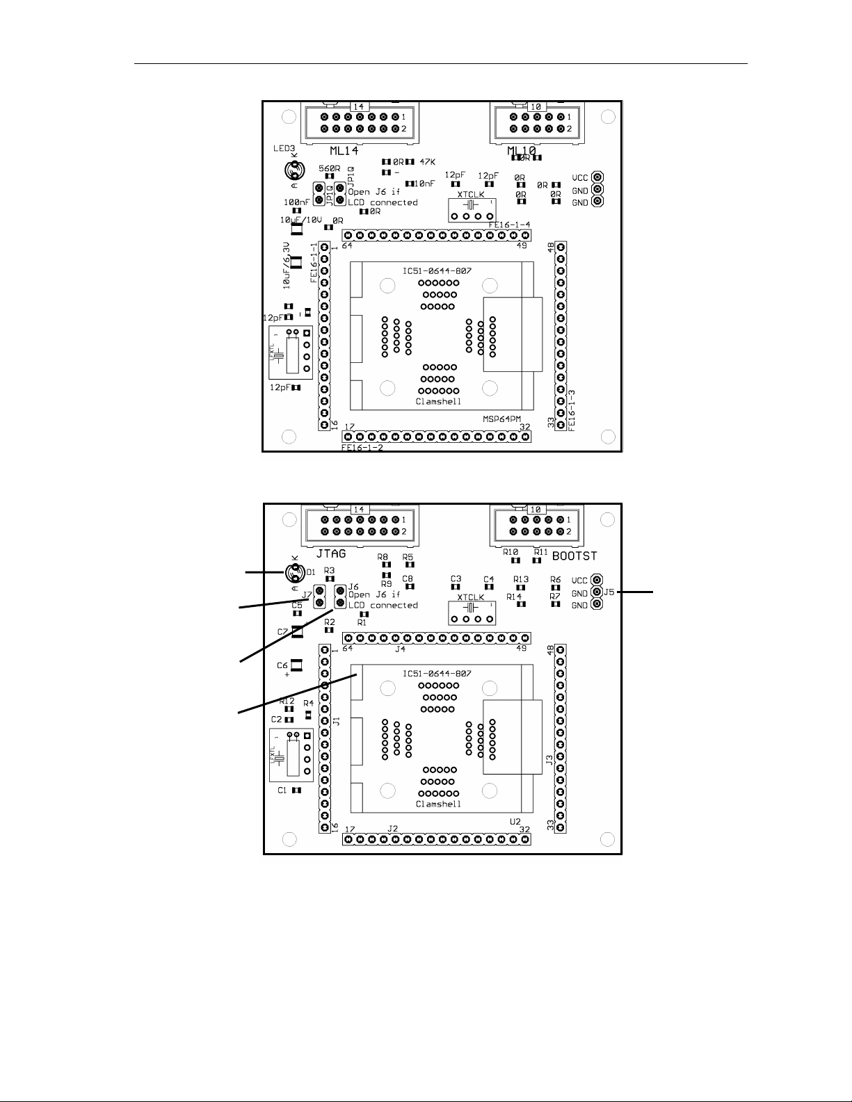
Hardware
LED connected to pin 12
Jumper J7
Open to measure current
Jumper J6
Open to disconnect LED
Orient Pin 1 of MSP430 device
Connector J5
External power connection
Remove R8 an d jumpe r R9
Figure B-10. MSP-TS430PM64 Target Socket module, PCB Pictorials, Rev. 1.1
B-11
Page 62

Hardware
B.1 History of changes to MSP-TS430PM64 Target Socket module
Changes from Rev. 0.1 to 1.0:
Connector J5 for external power was added
Connectors FETJ2 and FETJ3 were removed
C8 was changed from 100nF to 10nF
R5 was changed from 100k to 47k
R13 and R14 were added to support BSL usage on F413. They are not
assembled
R4 was removed
Changes from Rev. 1.0 to 1.1:
Connection JTAG/6 <-> J1/9: R4=0Ohm was inserted. R4 is not
assembled. This isolates XOUT from the JTAG connector.
On Rev. 0.1, power can be found or should be supplied on the target pins:
J1/1(DVcc), J4/16(AVcc), J4/15(DVss) and J4/14(AVss). Vcc can also
be applied to FETJ2-2 and Vss can also be applied to FETJ2-4.
B-12
Page 63

Hardware
Figure B-11. MSP-TSPN80 Target Socket module, Schematic
B-13
Page 64

Hardware
LED connected to pin 12
Jumper J6
Open to disconnect LED
Orient Pin 1 of MSP430 device
Jumper J7
Open to measure current
Connector J5
External power connection
Remove R8 an d jumpe r R9
B-14
Figure B-12. MSP-TSPN80 Target Socket module, PCB Pictorials
Page 65

Hardware
Note: Connections between the JTAG header and pins XOUT and XIN are no longer required, and
should not be made.
Figure B-13. MSP-TSPZ100 Target Socket module, Schematic
B-15
Page 66

Hardware
LED connected to pin 12
Connector J5
External power connection
Remove R8 and jumper R9
Orient Pin 1 of MSP430 device
Jumper J6
Open to disconnect LED
Jumper J7
Open to measure current
B-16
Figure B-14. MSP-TSPZ100 Target Socket module, PCB Pictorials
Page 67

Hardware
Figure B-15. MSP-FET430UIF USB Interface schematics
B-17
Page 68

Hardware
B-18
Page 69

Hardware
B-19
Page 70

Hardware
B-20
Page 71

Hardware
B-21 C-1
Page 72

Page 73

Appendix C
FET Specific Menus
This appendix describes the C-SPY menus that are specific to the FET.
Topic Page
C.1 EMULATOR C-2
C.1.1 EMULATOR->RELEASE JTAG ON GO C-2
C.1.2 EMULATOR->RESYNCHRONIZE JTAG C-2
C.1.3 EMULATOR->INIT NEW DEVICE C-2
C.1.4 EMULATOR->SHOW USED BREAKPOINTS C-2
C.1.5 EMULATOR->ADVANCED->GENERAL CLOCK CONTROL C-2
C.1.6 EMULATOR->ADVANCED->EMULATION MODE C-2
C.1.7 EMULATOR->ADVANCED->MEMORY DUMP C-3
C.1.8 EMULATOR->ADVANCED->BREAKPOINT COMBINER C-3
C.1.9 EMULATOR->STATE STORAGE C-3
C.1.10 EMULATOR->STATE STORAGE WINDOW C-3
C.1.11 EMULATOR->SEQUENCER C-3
C.1.12 EMULATOR->”POWER ON” RESET C-3
C.1.13 EMULATOR->SECURE C-3
C.1.14 EMULATOR->GIE on/off C-4
C.1.15 EMULATOR->LEAVE TARGET RUNNING C-4
C.1.16 EMULATOR->FORCE SINGLE STEPPING C-4
C.1.17 EMULATOR->SET VCC C-4
Page 74

FET Specific Menus
C.1 EMULATOR
The current device type is displayed.
C.1.1 EMULATOR->RELEASE JTAG ON GO
C-SPY uses the device JTAG signals to debug the device. On some MSP430
devices, these JTAG signals are shared with the device port pins. Normally, CSPY maintains the pins in JTAG mode so that the device can be debugged.
During this time the port functionality of the shared pins is not available.
However, when RELEASE JTAG ON GO is selected, the JTAG drivers are set
to tri-state and the device is released from JTAG control (TEST pin is set to
GND) when GO is activated. Any active on-chip breakpoints are retained and
the shared JTAG port pins revert to their port functions.
At this time, C-SPY has no access to the device and cannot determine if an
active breakpoint (if any) has been reached. C-SPY must be manually
commanded to stop the device, at which time the state of the device will be
determined (i.e., Was a breakpoint reached?).
Refer to FAQ, Debugging #10).
C.1.2 EMULATOR->RESYNCHRONIZE JTAG
Regain control of the device.
It is not possible to RESYNCHRONIZE JTAG while the device is operating.
C.1.3 EMULATOR->INIT NEW DEVICE
Initialize the device according to the settings in the DOWNLOAD OPTIONS.
Basically, the current program file is downloaded to the device memory. The
device is then reset. This option can be used to program multiple devices with
the same program from within the same C-SPY session.
It is not possible to select INIT NEW DEVICE while the device is operating.
C.1.4 EMULATOR->SHOW USED BREAKPOINTS
List all used hardware and virtual breakpoints, as well as all currently defined
EEM breakpoints.
C.1.5 EMULATOR->ADVANCED->GENERAL CLOCK CONTROL
Disable the specified system clock while C-SPY has control of the devi c e
(following a STOP or breakpoint). All system clocks are enabled following a GO
or a single step (STEP/STEP INTO). Refer to FAQ, Debugging #17).
C.1.6 EMULATOR->ADVANCED->EMULATION MODE
Specify the device to be emulated. The device must be reset (or reinitialized
through INIT NEW DEVICE) following a change to the emulation mode.
C-2
Page 75

Refer to Appendix D.
C.1.7 EMULATOR->ADVANCED->MEMORY DUMP
Write the specified device memory contents to a specified file. A conventional
dialog is displayed that permits the user to specify a file name, a memory
starting address, and a length. The addressed memory is then written in a text
format to the named file. Options permit the user to select word or byte text
format, and address information and register contents can also be appended to
the file.
C.1.8 EMULATOR->ADVANCED->BREAKPOINT COMBINER
Open the Breakpoint Combiner dialog box. The Breakpoint Combiner dialog
box permits one to specify breakpoint dependencies. A breakpoint will be
triggered when the breakpoints are encountered in the specified order.
C.1.9 EMULATOR->STATE STORAGE
Open the State Storage dialog box. The State Storage dialog box permits one
to use the state storage module. The state storage module is present only in
those devices that contain the EEM.
Refer to the IAR C-SPY FET Debugger section in the MSP430 IAR Embedded
Workbench IDE User Guide.
FET Specific Menus
C.1.10 EMULATOR->STATE STORAGE WINDOW
Open the State Storage window, and display the stored state information as
configured by the State Storage dialog.
Refer to the IAR C-SPY FET Debugger section in the MSP430 IAR Embedded
Workbench IDE User Guide.
C.1.11 EMULATOR->SEQUENCER
Open the Sequencer dialog box. The Sequencer dialog box permits one to
configure the sequencer state machine.
Refer to the IAR C-SPY FET Debugger section in the MSP430 IAR Embedded
Workbench IDE User Guide.
C.1.12 EMULATOR->”POWER ON” RESET
Cycle power to the device to effect a reset.
C.1.13 EMULATOR->SECURE
Programs the code security fuse. No further access via JTAG is possible.
C-3
Page 76

FET Specific Menus
C.1.14 EMULATOR->GIE on/off
Enables or disables all interrupts. Needs to be restored manually before GO.
C.1.15 EMULATOR->LEAVE TARGET RUNNING
If C-SPY is closed, the target keeps running the user program.
C.1.16 EMULATOR->FORCE SINGLE STEPPING
On GO the program is executed by single steps. Only in this mode the cycle
counter works correctly.
C.1.17 EMULATOR->SET VCC
On the USB FET the target supply voltage can be adjusted between 1.8V and
5.0V. This voltage is available on pin 2 of the 14-pin target connector to supply
the target from the USB FET. If the target is supplied externally, the external
supply voltage should be connected to pin 4 of the target connector, so the
USB FET can set the level of the output signals accordingly.
Note: Availability of EMULATOR->ADVANCED menus
Not all EMULATOR->ADVANCED menus are supported by all MSP430
devices. These menus will be grayed-out.
C-4
Page 77

Appendix D
80-pin MSP430F44x and MSP430F43x
Device Emulation
80-pin MSP430F44x and MSP430F43x devices can be emulated by the
100-pin MSP430F449 devi c e.
Table D-1. F4xx/80-pin Signal Mapping lists where the pin signals of an 80pin device appear on the pins of an MSP-TS430PZ100 Target Socket
module. Note: The MSP-TS430PZ100 must be modified as indicated.
Refer to Appendix C.1.6 EMULATOR->ADVANCED->EMULATION MODE
to enable the emulation mode.
Topic Page
D-2
D-1
Page 78

80-pin MSP430F44x and MSP430F43x Device Emulation
Table D-1. F4xx/80-pin Signal Mapping
F4xx/80-pin Signal F4xx/80-pin Pin
Number
DVcc1 1 1
P6.3/A3 2 2
P6.4/A4 3 3
P6.5/A5 4 4
P6.6/A6 5 5
P6.7/A7 6 6
VREF+ 7 7
XIN 8 8
XOUT 9 9
VeREF+ 10 10
VREF-/VeREF- 11 11
P5.1/S0 12 12
P5.0/S1 13 13
P4.7/S2 14 14 14-46
P4.6/S3 15 15 15-47
P4.5/S4 16 16 16-48
P4.4/S5 17 17 17-49
P4.3/S6 18 16 18-50
P4.2/S7 19 19 19-51
P4.1/S8 20 20 20-62
P4.0/S9 21 21 21-63
S10 22 22
S11 23 23
S12 24 24
S13 25 25
S14 26 26
S15 27 27
S16 28 28
S17 29 29
P2.7/ADC12CLK/S18 30 30
P2.6/CAOUT/S19 31 31
S20 32 32
S21 33 33
S22 34 34
S23 35 35
P3.7/S24 36 36 36-64
P3.6/S25 37 37 37-65
P3.5/S24 38 38 38-66
P3.4/S27 39 39 39-67
P3.3/UCLK0/S28 40 40 40-68
P3.2/SOMI0/S29 41 41 41-69
P3.1/SIMO0/S30 42 42 42-70
P3.0/STE0/S31 43 43 43-71
COM0 44 52†
P5.2/COM1 45 53
P5.3/COM2 46 54
P5.4/COM3 47 55
R03 48 56
MSP430TS430PZ100 Pin
Number
Connection
required
between
indicated pins of
MSP430TS430PZ100
socket
D-2
Page 79

80-pin MSP430F44x and MSP430F43x Device Emulation
P5.5/R13 49 57
P5.6/R23 50 58
P5.7/R33 51 59
DVcc2 52 60
DVss2 53 61
P2.5/URXD0 54 74†
P2.4/UTXD0 55 75
P2.3.TB2 56 76
P2.2/TB1 57 77
P2.1/TB0 58 78
P2.0/TA2 59 79
P1.7/CA1 60 80
P1.6/CA0 61 81
P1.5/TACLK/ACLK 62 82
P1.4/TBCLK/SMCLK 63 83
P1.3/TBOUTH/SVSOUT 64 84
P1.2/TA1 65 85
P1.1/TA0/MCLK 66 86
P1.0/TA0 67 87
XT2OUT 68 88
XT2IN 69 89
TDO/TDI 70 90
TDI 71 91
TMS 72 92
TCK 73 93
RST/NMI 74 94
P6.0/A0 75 95
P6.1/A1 76 96
P6.2/A2 77 97
Avss 78 98
DVss1 79 99
Avcc 80 100
† Note di scontinuity of pin numbering sequence
D-3
Page 80

Page 81

Appendix E
TI to IAR 2.x/3.x Assembler Migration
Texas Instruments made a suite of development tools for the MSP430,
including a comprehensive assembler and device simulator. The source of
the TI assembler and the source of the Kickstart assembler are not 100%
compatible; the instruction mnemonics are identical, while the assembler
directives are somewhat different. The following section documents the
differences between the TI assembler directives and the Kickstart 2.x/3.x
assembler directives.
Topic Page
E.1 Segment Control E-2
E.2 Translating Asm430 Assembler Directives to A430 Directives E-2
E.2.1 Introduction E-2
E.2.2 Character strings E-2
E.2.3 Section Control Directives E-3
E.2.4 Constant Initialization Directives E-4
E.2.5 Listing Control Directives E-4
E.2.6 File Reference Directives E-5
E.2.7 Conditional-Assembly Directives E-5
E.2.8 Symbol Control Directives E-6
E.2.9 Macro Directives E-7
E.2.10 Miscellaneous Directives E-7
E.2.11 Preprocessor Directives E-7
E.2.12 Alphabetical Listing and Cross Reference of Asm430
Directives
E-8
E.2.13 Additional A430 Directives (IAR) E-8
E-1
Page 82

TI to IAR 2.x/3.x Assembler Migration
E.1 Segment Control
RSEG defines a Relocatable SEGment. A relocatable segment means that
the code that follows the RSEG statement will be place *somewhere* in the
region defined for that segment (in the .xcl file). In other words, the code
can be "relocated", and you don't know (or care) where it's put. In the .xcl
files provided with the FET, multiple segments are defined in the same
memory regions. ASEG defines an Absolute SEGment. An absolute
segment means that the code that follows the ASEG statement will be
placed in the order it is encountered in the region defined for the segment
(in the .xcl file). In other words, the placement of the code is fixed in
memory. One significant difference between the new IAR assembler and
the old TI assembler is the meaning of the ORG statement. In the old TI
assembler, ORG would set the assembler code pointer to the specified
absolute address. However, the IAR assembler uses ORG to set an offset
from the current RSEG. Fortunately, if you don't use RSEG explicitly, it will
default to 0 (zero) and your program will link as you expect (with your code
at ORG). Be careful if you mix RSEG and ORG as ORG then becomes a
relative offset. Use ASEG if you want the (absolute) behavior of the old TI
ORG statement.
E.2 Translating Asm430 Assembler Directives to A430 Directives
E.2.1 Introduction
The following sections describe, in general, how to convert assembler
directives for Texas Instruments’ Asm430 assembler (Asm430) to
assembler directives for IAR’s A430 assembler (A430). These sections are
only intended to act as a guide for translation. For detailed descriptions of
each directive, refer to either the MSP430 Assembly Language Tools
User’s Guide, SLAUE12, from Texas Instruments, or the MSP430
Assembler User’s Guide from IAR.
Note: Only the assembler directives require conversion
Only the assembler directives require conversion - not the assembler
instructions. Both assemblers use the same instruction mnemonics,
operands, operators, and special symbols such as the section program
counter ($), and the comment delimiter (;).
The A430 assembler is not case sensitive by default. These sections show
the A430 directives written in uppercase to distinguish them from the
Asm430 directives, which are shown in lower case.
E.2.2 Character strings
In addition to using different directives, each assembler uses different
syntax for character strings. A430 uses C syntax for character strings: A
quote is represented using the backslash character as an escape character
together with quote (\”) and the backslash itself is represented by two
E-2
Page 83

TI to IAR 2.x/3.x Assembler Migration
consecutive backslashes (\\). In Asm430 syntax, a quote is represented by
two consecutive quotes (“”). See examples below:
Character String Asm430 Syntax (TI) A430 Syntax (IAR)
PLAN “C” “PLAN “”C””” “PLAN \”C\””
\dos\command.com “\dos\command.com” “\\dos\\command.com”
Concatenated string (i.e. Error 41) - “Error ” “41”
E.2.3 Section Control Directives
Asm430 has three predefined sections into which various parts of a
program are assembled. Unin iti al ized dat a is assem bl ed into the .bss
section, initialized data into the .data section and executable code into the
.text section.
A430 also uses sections or segments, but there are no predefined segment
names. Often, it is convenient to adhere to the names used by the C
compiler: DATA16_Z for uninitialized data, CONST for constant (initialized)
data and CODE for executable code. The table below uses these names.
A pair of segments can be used to make initialized, modifiable data PROMable. The ROM segment would contain the initializers and would be copied
to RAM segment by a start-up routine. In this case, the segments must be
exactly the same size and layout.
Description Asm430 Directive (TI) A430 Directive (IAR)
Reserve size bytes in the .bss
(uninitialized data) section
Assemble into the .data (initialized data)
section
Assemble into a named (initialized)
section
Assemble into the .text (executable code)
section
Reserve space in a named (uninitialized)
section
Alignment on byte boundary .align 2)
Alignment on word boundary .even EVEN
1) Space is reserved in an uninitialized segment by first switching to that segment, then defining the
appropriate memory block, and then switching back to the original segment. For example:
RSEG DATA16_Z
LABEL: DS 16
RSEG CODE
2) Initialization of bit-field constants (.field) is not supported, therefore, the section counter is always bytealigned.
.bss 1)
.data RSEG const
.sect RSEG
.text RSEG code
.usect 1)
Additional A430 Directives (IAR) A430 Directive (IAR)
Switch to an absolute segment ASEG
Switch to a relocatable segment RSEG
Switch to a common segment COMMON
Switch to a stack segment (high-to-low allocation) STACK
Alignment on specified address boundary (power of two) ALIGN
Set the location counter ORG
E-3
Page 84

TI to IAR 2.x/3.x Assembler Migration
E.2.4 Constant Initialization Directives
Description Asm430 Directive (TI) A430 Directive (IAR)
Initialize one or more successive bytes or
text strings
Initialize a 48-bit MSP430 floating-point
constant
Initialize a variable-length field .field 2)
Initialize a 32-bit MSP430 floating-point
constant
Reserve size bytes in the current section .space DS
Initialize one or more text strings .string DB
Initialize one or more 16-bit integers .word DW
1) The 48-bit MSP430 format is not supported
2) nitialization of bit-field constan ts (.field) is not supported. Constants must be combined into com plet e
words using DW.
; Asm430 code ; A430 code
.field 5,3 \
.field 12,4 | -> DW (30<<(4+3))|(12<<3)|5 ; equals 3941
.field 30,8 /
3) The 32-bit IEEE floating-point format, used by the C Compiler, is supported in the A430 assembler.
.byte or .string DB
.double 1)
.float DF 3)
Additional A430 Directives (IAR) A430 Directive (IAR)
Initialize one or more 32-bit integers DL
E.2.5 Listing Control Directives
Description Asm430 Directive (TI) A430 Directive (IAR)
Allow false conditional code block listing .fclist LSTCNDInhibit false conditional code block listing .fcnolist LSTCND+
Set the page length of the source listing .length PAGSIZ
Set the page width of the source listing .width COL
Restart the source listing .list LSTOUT+
Stop the source listing .nolist LSTOUTAllow macro listings and loop blocks .mlist LSTEXP+ (macro)
LSTREP+ (loop blocks)
Inhibit macro listings and loop blocks .mnolist LSTEXP- (macro)
LSTREP- (loop blocks)
Select output listing options .option 1)
Eject a page in the source listing .page PAGE
Allow expanded substitution symbol listing .sslist 2)
Inhibit expanded substitution symbol
listing
Print a title in the listing page header .title 3)
1) No A430 directive directly corresponds to .option. The individual listing control directives (above) or the
command-line option -c (with suboptions) should be used to replace the .option directive.
2) There is no directive that directly corresponds to .sslist/.ssnolist.
3) The title in the listing page header is the source file name.
.ssnolist 2)
Additional A430 Directives (IAR) A430 Directive (IAR)
Allow/inhibit listing of macro definitions LSTMAC (+/-)
Allow/inhibit multi-line code listing LSTCOD (+/-)
Allow/inhibit partitioning of listing into pages LSTPAG (+/-)
Generate cross reference table LSTXREF (+/-)
E-4
Page 85

TI to IAR 2.x/3.x Assembler Migration
E.2.6 F ile Referen ce Directives
Description Asm430 Directive (TI) A430 Directive (IAR)
Include source statements from another
file
Identify one or more symbols that are
defined in the current module and used in
other modules
Identify one or more global (external)
symbols
Define a macro library .mlib 2)
Identify one or more symbols that are
used in the current module but defined in
another module
1) The directive .global functions as either .def if the symbol is defined in the current module, or .ref
otherwise. PUBLIC or EXTERN must be used as applicable with the A430 assembler to replace the
.global directive.
2) The concept of macro libraries is not supported. Include files with macro definitions must be used for this
functionality.
Modules may be used with the Asm430 assembler to create individually
linkable routines. A file may contain multiple modules or routines. All
symbols except those created by DEFINE, #define (IAR preprocessor
directive) or MACRO are “undefined” at module end. Library modules are,
furthermore, linked conditionally. This means that a library module is only
included in the linked executable if a public symbol in the module is
referenced externally. The following directives are used to mark the
beginning and end of modules in the A430 assembler.
.copy or .include #include or $
.def PUBLIC or EXPORT
.global 1)
.ref EXTERN or IMPORT
Additional A430 Directives (IAR) A430 Directive (IAR)
Start a program module NAME or PROGRAM
Start a library module MODULE or LIBRARY
Terminate the current program or library module ENDMOD
E.2.7 Conditional-Assembly Directives
Description Asm430 Directive (TI) A430 Directive (IAR)
Optional repeatable block assembly .break 1)
Begin conditional assembly .if IF
Optional conditional assembly .else ELSE
Optional conditional assembly .elseif ELSEIF
End conditional assembly .endif ENDIF
End repeatable block assembly .endloop ENDR
Begin repeatable block assembly .loop REPT
1) There is no directive that directly corresponds to .break. However, the EXITM directive can be used with
other conditionals if repeatable block assembly is used in a macro, as shown:
SEQ MACRO FROM,TO ; Initialize a sequence of byte constants
LOCAL X
X SET FROM
REPT TO-FROM+1 ; Repeat from FROM to TO
IF X>255 ; Break if X exceeds 255
EXITM
ENDIF
DB X ; Initialize bytes to FROM...TO
E-5
Page 86

TI to IAR 2.x/3.x Assembler Migration
X SET X+1 ; Increment counter
ENDR
ENDM
Additional A430 Directives (IAR) A430 Directive (IAR)
Repeatable block assembly: Formal argument is substituted by each
character of a string.
Repeatable block assembly: formal argument is substituted by each string
of a list of actual arguments.
See also Preprocessor Directives
REPTC
REPTI
E.2.8 Symbol Control Directives
The scope of assembly-time symbols differs in the two assemblers. In
Asm430, definitions are global to a file, but can be undefined with the
.newblock directive. In A430, symbols are either local to a macro (LOCAL),
local to a module (EQU) or global to a file (DEFINE). In addition, the
preprocessor directive #define can also be used to define local symbols.
Description Asm430 Directive (TI) A430 Directive (IAR)
Assign a character string to a substitution
symbol
Undefine local symbols .newblock 1)
Equate a value with a symbol .equ or .set EQU or =
Perform arithmetic on numeric substitution
symbols
End structure definition .endstruct 2)
Begin a structure definition .struct 2)
Assign structure attributes to a label .tag 2)
1) No A430 directive directly corresponds to .newblock. However, #undef may be used to reset a symbol
that was defined with the #define directive. Also, macros or modules may be used to achieve the
.newblock functionality because local symbols are implicitly undefined at the end of a macro or module.
2) Definition of structure types is not supported. Similar functionality is achieved by using macros to allocate
aggregate data and base address plus symbol ic off set, as sh ow n below:
MYSTRUCT:MACRO
DS 4
ENDM
LO DEFINE 0
HI DEFINE 2
RSEG DATA16_Z
X MYSTRUCT
RSEG CODE
MOV X+LO,R4
...
.asg SET or VAR or ASSIGN
.eval SET or VAR or ASSIGN
Additional A430 Directives (IAR) A430 Directive (IAR)
Define a file-wide symbol DEFINE
Definition of special function registers (byte size) SFRB
Definition of special function registers (word size) SFRW
E-6
Page 87

TI to IAR 2.x/3.x Assembler Migration
E.2.9 Macro Directives
Description Asm430 Directive (TI) A430 Directive (IAR)
Define a macro .macro MACRO
Exit prematurely from a macro .mexit EXITM
End macro definition .endm ENDM
Additional A430 Directives (IAR) A430 Directive (IAR)
Create symbol, local to a macro LOCAL 1)
1) In Asm430 local symbols are suffixed by a question mark (?).
E.2.10 Miscellaneous Directives
Description Asm430 Directive (TI) A430 Directive (IAR)
Send user-defined error messages to the
output device
Send user-defined messages to the output
device
Send user-defined warning messages to
the output device
Define a load address label .label 3)
Directive produced by absolute lister .setsect ASEG 4)
Directive produced by absolute lister .setsym EQU or = 4)
Program end .end END
1) The syntax of the #message directive is: #message “<string>”
This causes ‘#message <string>’ to be output to the project build window during assemble/compile time.
2) Warning messages cannot be user-defined. #message may be used, but the warning counter will not be
incremented.
3) The concept of load-time addresses is not supported. Run-time and load-time addresses are assumed to
be the same. To achieve the same effect, labels can be given absolute (run-time) addresses by the EQU
directives.
; Asm430 code ; A430 code
.label load_start load_start:
Run_start: <code>
<code> load_end:
Run_end: run_start:EQU 240H
.label load_end run_end: EQU run_start+load_end-load_start
4) Although not produced by the absolute lister ASEG defines absolute segments and EQU can be used to
define absolute symbols.
MYFLAG EQU 23EH ; MYFLAG is located at 23E
ASEG 240H ; Absolute segment at 240
MAIN: MOV #23CH, SP ; MAIN is located at 240
...
Additional A430 Directives (IAR) A430 Directive (IAR)
Set the default base of constants RADIX
Enable case sensitivity CASEON
Disable case sensitivity CASEOFF
.emsg #error
.mmsg #message 1)
.wmsg 2)
E.2.11 Preprocessor Directives
The A430 assembler includes a preprocessor similar to that used in C
programming. The following preprocessor directives can be used in include
files which are shared by assembly and C programs.
E-7
Page 88

TI to IAR 2.x/3.x Assembler Migration
Additional A430 Directives (IAR) A430 Directive (IAR)
Assign a value to a preprocessor symbol #define
Undefine a preprocessor symbol #undef
Conditional assembly #if, #else, #elif
Assemble if a preprocessor symbol is defined (not defined) #ifdef, #ifndef
End a #if, #ifdef or #ifndef block #endif
Includes a file #include
Generate an error #error
E.2.12 Alphabetical Listing and Cross Reference of Asm430 Directives
Asm430 directive A430 directive Asm430 directive A430 directive
.align See Section control directives .loop REPT
.asg SET or VAR or ASSIGN .macro MACRO
.break See Conditional-Assembly Directives .mexit EXITM
.bss See Symbol Control Directives .mlib See File Referencing Directives
.byte or .string DB .mlist LSTEXP+ (macro)
.copy or .include #include or $ LSTREP+ (loop blocks)
.data RSEG .mmsg #message (XXXXXX)
.def PUBLIC or EXPORT .mnolist LSTEXP- (macro)
.double Not supported LSTREP- (loop blocks)
.else ELSE .newblock See Symbol Control Directives
.elseif ELSEIF .nolist LSTOUT.emsg #error .option See Listing Control Directives
.end END .page PAGE
.endif ENDIF .ref EXTERN or IMPORT
.endloop ENDR .sect RSEG
.endm ENDM .setsect See Miscellaneous Directives
.endstruct See Symbol Control Directives .setsym See Miscellaneous Directives
.equ or .set EQU or = .space DS
.eval SET or VAR or ASSIGN .sslist Not supported
.even EVEN .ssnolist Not supported
.fclist LSTCND- .string DB
.fcnolist LSTCND+ .struct See Symbol Control Directives
.field See Constant Initialization Directives .tag See Symbol Control Directives
.float See Constant Initialization Directives .text RSEG
.global See File Referencing Directives .title See Listing Control Directives
.if IF .usect See Symbol Control Directives
.label See Miscellaneous Directives .width COL
.length PAGSIZ .wmsg See Miscellaneous Directives
.list LSTOUT+ .word DW
E.2.13 Additional A430 Directives (IAR)
Conditional-Assembly Directives Constant Initialization Directives Macro Directives
REPTC DL LOCAL
REPTI
File Referencing Directives Miscellaneous Directives Symbol Control Directives
NAME or PROGRAM RADIX DEFINE
MODULE or LIBRARY CASEON SFRB
ENDMOD CASEOFF SFRW
Listing Control Directives Preprocessor Directives Symbol Control Directives
LSTMAC (+/-) #define ASEG
LSTCOD (+/-) #undef RSEG
E-8
Page 89

TI to IAR 2.x/3.x Assembler Migration
LSTPAG (+/-) #if, #else, #elif COMMON
LSTXREF (+/-) #ifdef, #ifndef STACK
#endif ALIGN
#include ORG
#error
E-9
Page 90

Page 91

Appendix F
MSP-FET430UIF Installation Guide
This section describes the hardware installation process of the MSPFET430UIF USB debug interfac e on a PC running Wi ndows XP. The
installation procedure for a Windows 2000 system is very similar and
therefore not shown here.
Topic Page
F.1 Hardware Installation F-2
F-1
Page 92

MSP-FET430UIF Installation Guide
F.1 Hardware Installation
1) Connect the MSP-FET430UIF USB Debug Interface with a USB cable
to a USB port of your PC
2) Windows now should recognize the new hardware as an “MSP430
USB FET x.xx.xx” (Figure F-1).
Figure F-1. WinXP Hardware Recognition
3) The Hardware Wizard should start automatically and popup the “Found
New Hardware Wizard” dialog window.
4) Instruct the Wizard to install the hardware driver from a specific
location (Figure F-2).
F-2
Figure F-2. WinXP Hardware Wizard
5) Point the Hardware Wizard to the according folder where the
corresponding driver information files are located on your hard disc.
Page 93

MSP-FET430UIF Installation Guide
Figure F-3. WinXP Driver Location Selection Folder
6) The Wizard should generate a message that an appropriate driver has
been found.
7) Note that WinXP shows a warning that the driver is not certified by
Microsoft. Ignore this warning and click “Continue Anyway” (Figure
F-4).
F-3
Page 94

MSP-FET430UIF Installation Guide
Figure F-4. WinXP Driver Installation
8) In the next step the Wizard installs the driver files.
9) The Wizard now shows a message that it has finished the installation
of the software for “MSP430 USB FET Adapter”.
10) After closing the Hardware Wizard, Windows automatically recognizes
another new hardware device called “Texas Instruments UMP Serial
Port”.
11) Depending on the current update version of the OS corresponding
drivers are installed automatically or the Hardware Wizard pops up
again. In case of the Wizard is started, please repeat the steps already
described above again
12) Finally the MSP-FET430UIF debug interface is installed and ready to
use. The Device Manager should list a new entry as shown in Figure
F-5.
F-4
Page 95

MSP-FET430UIF Installation Guide
Figure F-5. Device Manager
F-5
 Loading...