

查询LMV331供应商
LMV331 SINGLE, LMV393 DUAL, LMV339 QUAD
GENERAL-PURPOSE LOW-VOLTAGE COMPARATORS
SLCS136C – AUGUST 1999 – REVISED APRIL 2000
D
2.7-V and 5-V Performance
D
Low Supply Current:
LMV331 ...60 µA Typ
LMV393 . . . 100 µA Typ
LMV339 . . . 170 µA Typ
D
Input Common-Mode Voltage Range
Includes Ground
D
Low Output Saturation Voltage
. . . 200 mV Typ
D
Package Options Include Plastic
Small-Outline (D), Small-Outline Transistor
(SOT-23 DBV, SC-70 DCK), and Thin Shrink
Small-Outline (PW) Packages
description
The LMV393 and LMV339 devices are
low-voltage (2.7 V to 5.5 V) versions of the dual
and quad comparators, LM393 and LM339, which
operate from 5 V to 30 V. The LMV331 is the
single-comparator version.
The LMV331, LMV339, and LMV393 are the most
cost-effective solutions for applications where
low-voltage operation, low power, space saving,
and price are the primary specifications in circuit
design for portable consumer products. These
devices offer specifications that meet or exceed
the familiar LM339 and LM393 devices at a
fraction of the supply current.
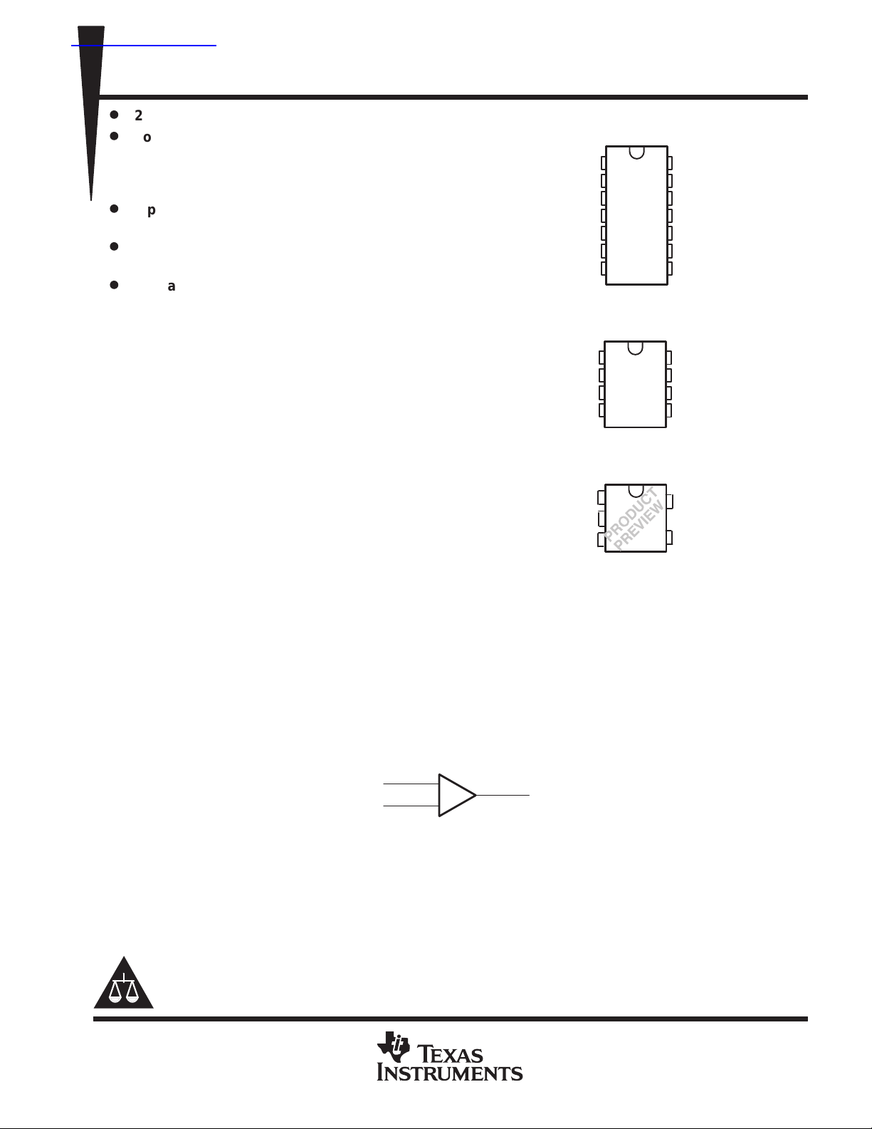
LMV339 ...D OR PW PACKAGE
2OUT
1OUT
LMV393 ...D OR PW PACKAGE
1OUT
LMV331 .. . DBV OR DCK PACKAGE
GND
V
CC+
1IN–
1IN+
2IN–
2IN+
1IN–
1IN+
GND
IN+
IN–
(TOP VIEW)
14
1
13
2
12
3
11
4
10
5
6
7
(TOP VIEW)
1
2
3
4
(TOP VIEW)
1
2
3
9
8
8
7
6
5
5
4
3OUT
4OUT
GND
4IN+
4IN–
3IN+
3IN–
V
CC+
2OUT
2IN–
2IN+
V
CC+
OUT
The LMV331 is available in the ultra-small DCK package, which is approximately one-half the size of the five-pin
DBV package. The DCK package saves space on printed circuit boards and enables the design of small
portable electronic devices. It also allows the designer to place the device closer to the signal source to reduce
noise pickup and increase signal integrity.
The LMV331I, LMV339I, and LMV393I devices are characterized for operation from –40°C to 85°C.
logic symbol (each comparator)
_
+
OUT
Copyright 2000, Texas Instruments Incorporated
Please be aware that an important notice concerning availability, standard warranty, and use in critical applications of
Texas Instruments semiconductor products and disclaimers thereto appears at the end of this data sheet.
UNLESS OTHERWISE NOTED this document contains PRODUCTION
DATA information current as of publication date. Products conform to
specifications per the terms of Texas Instruments standard warranty.
Production processing does not necessarily include testing of all
parameters.
IN–
IN+
POST OFFICE BOX 655303 • DALLAS, TEXAS 75265
1
LMV331 SINGLE, LMV393 DUAL, LMV339 QUAD
T
GENERAL-PURPOSE LOW-VOLTAGE COMPARATORS
SLCS136C – AUGUST 1999 – REVISED APRIL 2000
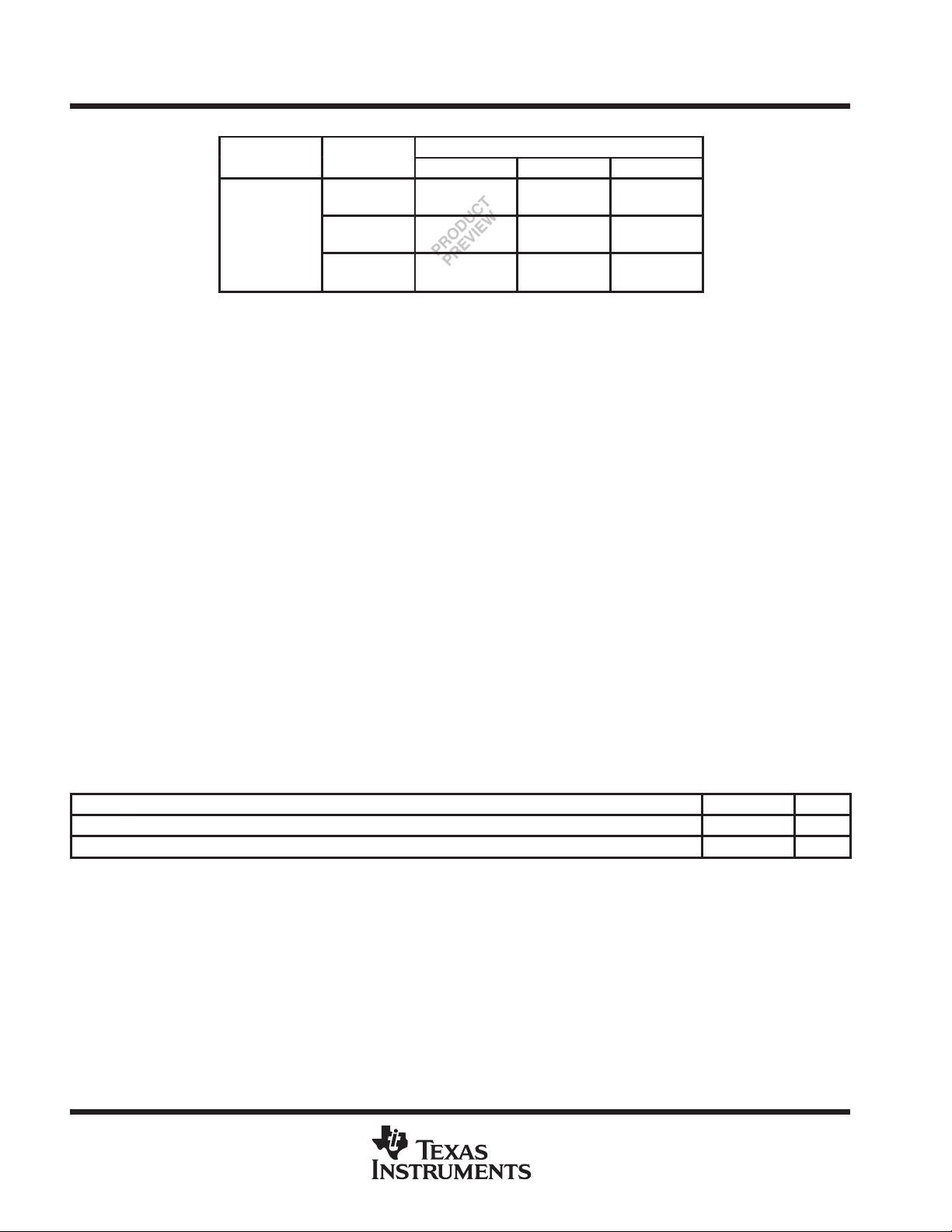
AVAILABLE OPTIONS
A
–40°C to 85°C
The D package is available taped and reeled. Add the suffix R to the device type (e.g.,
LMV393DR). The DCK, DBV, and PW packages are only available left-end taped and
reeled.
PACKAGE
TYPE
5-pin SOT
8-pin SOIC
8-pin TSSOP
14-pin SOIC
14-pin TSSOP
SINGLE DUAL QUADRUPLE
LMV331IDCKR
LMV331IDBVR
PACKAGED DEVICES
—
—
—
—
—
—
LMV393ID
LMV393IPWR
—
—
—
—
—
LMV339ID
LMV339IPWR
absolute maximum ratings over operating free-air temperature range (unless otherwise noted)
Supply voltage, V
Differential input voltage, VID (see Note 2) ±5.5 V. . . . . . . . . . . . . . . . . . . . . . . . . . . . . . . . . . . . . . . . . . . . . . . . . .
Input voltage range, VI (either input) 0 to 5.5°C. . . . . . . . . . . . . . . . . . . . . . . . . . . . . . . . . . . . . . . . . . . . . . . . . . . . .
Operating virtual junction temperature range 0 to 150°C. . . . . . . . . . . . . . . . . . . . . . . . . . . . . . . . . . . . . . . . . . . .
Package thermal impedance, θJA (see Notes 3 and 4): D (8-pin) package 97°C/W. . . . . . . . . . . . . . . . . . . . . .
Lead temperature 1,6 mm (1/16 inch) from case for 10 seconds: D or PW package 260°C. . . . . . . . . . . . . . .
Storage temperature range, T
†
Stresses beyond those listed under “absolute maximum ratings” may cause permanent damage to the device. These are stress ratings only, and
functional operation of the device at these or any other conditions beyond those indicated under “recommended operating conditions” is not
implied. Exposure to absolute-maximum-rated conditions for extended periods may affect device reliability.
NOTES: 1. All voltage values (except differential voltages and V
2. Differential voltages are at IN+ with respect to IN–.
3. Maximum power dissipation is a function of TJ(max),
ambient temperature is PD = (TJ(max) – TA)/
4. The package thermal impedance is calculated in accordance with JESD 51.
(see Note 1) 5.5 V. . . . . . . . . . . . . . . . . . . . . . . . . . . . . . . . . . . . . . . . . . . . . . . . . . . . . . . . . .
CC+
D (14-pin) package 86°C/W. . . . . . . . . . . . . . . . . . . .
DBV package 347°C/W. . . . . . . . . . . . . . . . . . . . . . .
DCK package 389°C/W. . . . . . . . . . . . . . . . . . . . . . .
PW (8-pin) package 149°C/W. . . . . . . . . . . . . . . . . .
PW (14-pin) package 113°C/W. . . . . . . . . . . . . . . . . .
–65 to 150°C. . . . . . . . . . . . . . . . . . . . . . . . . . . . . . . . . . . . . . . . . . . . . . . . . . . . .
stg
specified for the measurement of IOS) are with respect to the network GND.
CC+
θ
, and TA. The maximum allowable power dissipation at any allowable
θ
JA
JA
. Selecting the maximum of 150°C can affect reliability.
recommended operating conditions
MIN MAX UNIT
V
T
Supply voltage (single-supply operation) 2.7 5.5 V
CC+
Operating free-air temperature –40 85 °C
A
†
PRODUCT PREVIEW information concerns products in the formative or
design phase of development. Characteristic data and other
specifications are design goals. Texas Instruments reserves the right to
change or discontinue these products without notice.
2
POST OFFICE BOX 655303 • DALLAS, TEXAS 75265

IIBInput bias current
nA
IIOInput offset current
nA
Output leakage current
A
t
Propagation dela
high- to low-level output switching
ns
t
Propagation dela
high-level output switching
ns
LMV331 SINGLE, LMV393 DUAL, LMV339 QUAD
GENERAL-PURPOSE LOW-VOLTAGE COMPARATORS
SLCS136C – AUGUST 1999 – REVISED APRIL 2000
electrical characteristics at specified free-air temperature, V
otherwise noted)
PARAMETER TEST CONDITIONS T
V
a
I
O
V
V
I
CC
†
This device is product preview.
switching characteristics, TA = 25°C, V
PHL
PLH
Input offset voltage 25°C 1.7 7 mV
IO
Average temperature coefficient
V
IO
of input offset voltage
p
p
Output current VO ≤ 1.5 V 25°C 5 23 mA
p
Common-mode input voltage range 25°C –0.1 to 2 V
ICR
Saturation voltage IO ≤ 1 mA 25°C 200 mV
SAT
Supply current
p
p
PARAMETER TEST CONDITIONS MIN TYP MAX UNIT
y,
y, low- to
p
p
†
LMV331
LMV393 (both comparators)
LMV339 (all four comparators) 25°C 140 200
CC+
= 2.7 V, R
= 5.1 kΩ, GND = 0 V (unless otherwise noted)
L
Input overdrive = 10 mV 1000
Input overdrive = 100 mV 350
Input overdrive = 10 mV 500
Input overdrive = 100 mV 400
–40°C to 85°C 5
–40°C to 85°C 400
–40°C to 85°C 150
–40°C to 85°C 1
= 2.7 V, GND = 0 V (unless
CC+
A
25°C 10 250
25°C 5 50
25°C 0.003
25°C 40 100
25°C 70 140
MIN TYP MAX UNIT
m
V/°C
m
m
A
PRODUCT PREVIEW information concerns products in the formative or
design phase of development. Characteristic data and other
specifications are design goals. Texas Instruments reserves the right to
change or discontinue these products without notice.
POST OFFICE BOX 655303 • DALLAS, TEXAS 75265
3

LMV331 SINGLE, LMV393 DUAL, LMV339 QUAD
VIOInput offset voltage
mV
IIBInput bias current
nA
IIOInput offset current
nA
Output leakage current
A
V
Saturation voltage
I
mA
mV
LMV331
†
ICCSupply current
LMV393 (both comparators)
A
LMV339 (all four comparators)
t
Propagation dela
high- to low-level output switching
ns
t
Propagation dela
high-level output switching
ns
GENERAL-PURPOSE LOW-VOLTAGE COMPARATORS
SLCS136C – AUGUST 1999 – REVISED APRIL 2000
electrical characteristics at specified free-air temperature, V
noted)
PARAMETER TEST CONDITIONS T
p
a
I
O
V
A
†
This device is product preview.
Average temperature coefficient
V
IO
of input offset voltage
p
p
Output current VO ≤ 1.5 V 25°C 10 84 mA
p
Common-mode input voltage range 25°C –0.1 to 4.2 V
ICR
Large-signal differential voltage gain 25°C 20 50 V/mV
VD
SAT
pp
O
≤ 4
p
p
= 5 V , GND = 0 V (unless otherwise
CC+
A
25°C 1.7 7
–40°C to 85°C 9
25°C 5
25°C 25 250
–40°C to 85°C 400
25°C 2 50
–40°C to 85°C 150
25°C 0.003
–40°C to 85°C 1
25°C 200 400
–40°C to 85°C 700
25°C 60 120
–40°C to 85°C 150
25°C 100 200
–40°C to 85°C 250
25°C 170 300
–40°C to 85°C 350
MIN TYP MAX UNIT
m
V/°C
m
m
switching characteristics, TA = 25°C, V
PARAMETER TEST CONDITIONS MIN TYP MAX UNIT
PHL
PLH
p
p
y,
y, low- to
p
p
CC+
= 5 V, R
= 5.1 kΩ, GND = 0 V (unless otherwise noted)
L
Input overdrive = 10 mV 600
Input overdrive = 100 mV 200
Input overdrive = 10 mV 450
Input overdrive = 100 mV 300
PRODUCT PREVIEW information concerns products in the formative or
design phase of development. Characteristic data and other
specifications are design goals. Texas Instruments reserves the right to
change or discontinue these products without notice.
4
POST OFFICE BOX 655303 • DALLAS, TEXAS 75265

IMPORTANT NOTICE
T exas Instruments and its subsidiaries (TI) reserve the right to make changes to their products or to discontinue
any product or service without notice, and advise customers to obtain the latest version of relevant information
to verify, before placing orders, that information being relied on is current and complete. All products are sold
subject to the terms and conditions of sale supplied at the time of order acknowledgment, including those
pertaining to warranty, patent infringement, and limitation of liability.
TI warrants performance of its semiconductor products to the specifications applicable at the time of sale in
accordance with TI’s standard warranty. Testing and other quality control techniques are utilized to the extent
TI deems necessary to support this warranty . Specific testing of all parameters of each device is not necessarily
performed, except those mandated by government requirements.
Customers are responsible for their applications using TI components.
In order to minimize risks associated with the customer’s applications, adequate design and operating
safeguards must be provided by the customer to minimize inherent or procedural hazards.
TI assumes no liability for applications assistance or customer product design. TI does not warrant or represent
that any license, either express or implied, is granted under any patent right, copyright, mask work right, or other
intellectual property right of TI covering or relating to any combination, machine, or process in which such
semiconductor products or services might be or are used. TI’s publication of information regarding any third
party’s products or services does not constitute TI’s approval, warranty or endorsement thereof.
Copyright 2000, Texas Instruments Incorporated
 Loading...