


PRELIMINARY
LM3S617 Microcontroller
DATA SHEET
Copyright © 2007 Luminary Micro, Inc.DS-LM3S617-1972

Legal Disclaimers and Trademark Information
INFORMATION IN THIS DOCUMENT IS PROVIDED IN CONNECTION WITH LUMINARY MICRO PRODUCTS. NO LICENSE, EXPRESS OR
IMPLIED, BY ESTOPPEL OR OTHERWISE, TO ANY INTELLECTUAL PROPERTY RIGHTS IS GRANTED BY THIS DOCUMENT. EXCEPT
AS PROVIDED IN LUMINARY MICRO'S TERMS AND CONDITIONS OF SALE FOR SUCH PRODUCTS, LUMINARY MICRO ASSUMES NO
LIABILITY WHATSOEVER,AND LUMINARYMICRO DISCLAIMS ANY EXPRESS OR IMPLIED WARRANTY,RELATING TO SALE AND/OR
USE OF LUMINARY MICRO'S PRODUCTS INCLUDING LIABILITY OR WARRANTIES RELATING TO FITNESS FOR A PARTICULAR
PURPOSE, MERCHANTABILITY, OR INFRINGEMENT OF ANY PATENT, COPYRIGHT OR OTHER INTELLECTUAL PROPERTY RIGHT.
LUMINARY MICRO'S PRODUCTS ARE NOT INTENDED FOR USE IN MEDICAL, LIFE SAVING, OR LIFE-SUSTAINING APPLICATIONS.
Luminary Micro may make changes to specications and product descriptions at any time, without notice. Contact your local Luminary Micro sales ofce
or your distributor to obtain the latest specications before placing your product order.
Designers must not rely on the absence or characteristics of any features or instructions marked "reserved" or "undened." Luminary Micro reserves these
for future denition and shall have no responsibility whatsoever for conicts or incompatibilities arising from future changes to them.
Copyright © 2007 Luminary Micro, Inc. All rights reserved. Stellaris, Luminary Micro, and the Luminary Micro logo are registered trademarks of
Luminary Micro, Inc. or its subsidiaries in the United States and other countries. ARM and Thumb are registered trademarks and Cortex is a trademark
of ARM Limited. Other names and brands may be claimed as the property of others.
Luminary Micro, Inc.
108 Wild Basin, Suite 350
Austin, TX 78746
Main: +1-512-279-8800
Fax: +1-512-279-8879
http://www.luminarymicro.com
Preliminary
November 29, 20072

LM3S617 Microcontroller
Table of Contents
About This Document .................................................................................................................... 17
Audience .............................................................................................................................................. 17
About This Manual ................................................................................................................................ 17
Related Documents ............................................................................................................................... 17
Documentation Conventions .................................................................................................................. 17
1 Architectural Overview ...................................................................................................... 19
1.1 Product Features ...................................................................................................................... 19
1.2 Target Applications .................................................................................................................... 24
1.3 High-Level Block Diagram ......................................................................................................... 24
1.4 Functional Overview .................................................................................................................. 25
1.4.1 ARM Cortex™-M3 ..................................................................................................................... 26
1.4.2 Motor Control Peripherals .......................................................................................................... 26
1.4.3 Analog Peripherals .................................................................................................................... 27
1.4.4 Serial Communications Peripherals ............................................................................................ 28
1.4.5 System Peripherals ................................................................................................................... 28
1.4.6 Memory Peripherals .................................................................................................................. 29
1.4.7 Additional Features ................................................................................................................... 29
1.4.8 Hardware Details ...................................................................................................................... 30
1.4.9 System Block Diagram .............................................................................................................. 31
2 ARM Cortex-M3 Processor Core ...................................................................................... 32
2.1 Block Diagram .......................................................................................................................... 33
2.2 Functional Description ............................................................................................................... 33
2.2.1 Serial Wire and JTAG Debug ..................................................................................................... 33
2.2.2 Embedded Trace Macrocell (ETM) ............................................................................................. 34
2.2.3 Trace Port Interface Unit (TPIU) ................................................................................................. 34
2.2.4 ROM Table ............................................................................................................................... 34
2.2.5 Memory Protection Unit (MPU) ................................................................................................... 34
2.2.6 Nested Vectored Interrupt Controller (NVIC) ................................................................................ 34
3 Memory Map ....................................................................................................................... 38
4 Interrupts ............................................................................................................................ 40
5 JTAG Interface .................................................................................................................... 42
5.1 Block Diagram .......................................................................................................................... 43
5.2 Functional Description ............................................................................................................... 43
5.2.1 JTAG Interface Pins .................................................................................................................. 44
5.2.2 JTAG TAP Controller ................................................................................................................. 45
5.2.3 Shift Registers .......................................................................................................................... 46
5.2.4 Operational Considerations ........................................................................................................ 46
5.3 Initialization and Configuration ................................................................................................... 47
5.4 Register Descriptions ................................................................................................................ 48
5.4.1 Instruction Register (IR) ............................................................................................................. 48
5.4.2 Data Registers .......................................................................................................................... 50
6 System Control ................................................................................................................... 52
6.1 Functional Description ............................................................................................................... 52
6.1.1 Device Identification .................................................................................................................. 52
Preliminary
3November 29, 2007

Table of Contents
6.1.2 Reset Control ............................................................................................................................ 52
6.1.3 Power Control ........................................................................................................................... 55
6.1.4 Clock Control ............................................................................................................................ 55
6.1.5 System Control ......................................................................................................................... 58
6.2 Initialization and Configuration ................................................................................................... 58
6.3 Register Map ............................................................................................................................ 59
6.4 Register Descriptions ................................................................................................................ 60
7 Internal Memory ............................................................................................................... 110
7.1 Block Diagram ........................................................................................................................ 110
7.2 Functional Description ............................................................................................................. 110
7.2.1 SRAM Memory ........................................................................................................................ 110
7.2.2 Flash Memory ......................................................................................................................... 111
7.3 Flash Memory Initialization and Configuration ........................................................................... 113
7.3.1 Changing Flash Protection Bits ................................................................................................ 113
7.3.2 Flash Programming ................................................................................................................. 114
7.4 Register Map .......................................................................................................................... 114
7.5 Flash Register Descriptions (Flash Control Offset) ..................................................................... 115
7.6 Flash Register Descriptions (System Control Offset) .................................................................. 122
8 General-Purpose Input/Outputs (GPIOs) ....................................................................... 126
8.1 Block Diagram ........................................................................................................................ 127
8.2 Functional Description ............................................................................................................. 127
8.2.1 Data Control ........................................................................................................................... 128
8.2.2 Interrupt Control ...................................................................................................................... 129
8.2.3 Mode Control .......................................................................................................................... 130
8.2.4 Pad Control ............................................................................................................................. 130
8.2.5 Identification ........................................................................................................................... 130
8.3 Initialization and Configuration ................................................................................................. 130
8.4 Register Map .......................................................................................................................... 131
8.5 Register Descriptions .............................................................................................................. 133
9 General-Purpose Timers ................................................................................................. 165
9.1 Block Diagram ........................................................................................................................ 165
9.2 Functional Description ............................................................................................................. 166
9.2.1 GPTM Reset Conditions .......................................................................................................... 166
9.2.2 32-Bit Timer Operating Modes .................................................................................................. 167
9.2.3 16-Bit Timer Operating Modes .................................................................................................. 168
9.3 Initialization and Configuration ................................................................................................. 172
9.3.1 32-Bit One-Shot/Periodic Timer Mode ....................................................................................... 172
9.3.2 32-Bit Real-Time Clock (RTC) Mode ......................................................................................... 173
9.3.3 16-Bit One-Shot/Periodic Timer Mode ....................................................................................... 173
9.3.4 16-Bit Input Edge Count Mode ................................................................................................. 174
9.3.5 16-Bit Input Edge Timing Mode ................................................................................................ 174
9.3.6 16-Bit PWM Mode ................................................................................................................... 175
9.4 Register Map .......................................................................................................................... 175
9.5 Register Descriptions .............................................................................................................. 176
10 Watchdog Timer ............................................................................................................... 201
10.1 Block Diagram ........................................................................................................................ 201
10.2 Functional Description ............................................................................................................. 201
Preliminary
November 29, 20074

LM3S617 Microcontroller
10.3 Initialization and Configuration ................................................................................................. 202
10.4 Register Map .......................................................................................................................... 202
10.5 Register Descriptions .............................................................................................................. 203
11 Analog-to-Digital Converter (ADC) ................................................................................. 224
11.1 Block Diagram ........................................................................................................................ 225
11.2 Functional Description ............................................................................................................. 225
11.2.1 Sample Sequencers ................................................................................................................ 225
11.2.2 Module Control ........................................................................................................................ 226
11.2.3 Hardware Sample Averaging Circuit ......................................................................................... 227
11.2.4 Analog-to-Digital Converter ...................................................................................................... 227
11.2.5 Test Modes ............................................................................................................................. 227
11.2.6 Internal Temperature Sensor .................................................................................................... 227
11.3 Initialization and Configuration ................................................................................................. 228
11.3.1 Module Initialization ................................................................................................................. 228
11.3.2 Sample Sequencer Configuration ............................................................................................. 228
11.4 Register Map .......................................................................................................................... 229
11.5 Register Descriptions .............................................................................................................. 230
12 Universal Asynchronous Receivers/Transmitters (UARTs) ......................................... 257
12.1 Block Diagram ........................................................................................................................ 258
12.2 Functional Description ............................................................................................................. 258
12.2.1 Transmit/Receive Logic ........................................................................................................... 258
12.2.2 Baud-Rate Generation ............................................................................................................. 259
12.2.3 Data Transmission .................................................................................................................. 260
12.2.4 FIFO Operation ....................................................................................................................... 260
12.2.5 Interrupts ................................................................................................................................ 260
12.2.6 Loopback Operation ................................................................................................................ 261
12.3 Initialization and Configuration ................................................................................................. 261
12.4 Register Map .......................................................................................................................... 262
12.5 Register Descriptions .............................................................................................................. 263
13 Synchronous Serial Interface (SSI) ................................................................................ 295
13.1 Block Diagram ........................................................................................................................ 295
13.2 Functional Description ............................................................................................................. 295
13.2.1 Bit Rate Generation ................................................................................................................. 296
13.2.2 FIFO Operation ....................................................................................................................... 296
13.2.3 Interrupts ................................................................................................................................ 296
13.2.4 Frame Formats ....................................................................................................................... 297
13.3 Initialization and Configuration ................................................................................................. 304
13.4 Register Map .......................................................................................................................... 305
13.5 Register Descriptions .............................................................................................................. 306
14 Analog Comparator ......................................................................................................... 332
14.1 Block Diagram ........................................................................................................................ 332
14.2 Functional Description ............................................................................................................. 332
14.2.1 Internal Reference Programming .............................................................................................. 333
14.3 Initialization and Configuration ................................................................................................. 334
14.4 Register Map .......................................................................................................................... 335
14.5 Register Descriptions .............................................................................................................. 335
Preliminary
5November 29, 2007

Table of Contents
15 Pulse Width Modulator (PWM) ........................................................................................ 343
15.1 Block Diagram ........................................................................................................................ 343
15.2 Functional Description ............................................................................................................. 343
15.2.1 PWM Timer ............................................................................................................................. 343
15.2.2 PWM Comparators .................................................................................................................. 344
15.2.3 PWM Signal Generator ............................................................................................................ 345
15.2.4 Dead-Band Generator ............................................................................................................. 346
15.2.5 Interrupt/ADC-Trigger Selector ................................................................................................. 346
15.2.6 Synchronization Methods ......................................................................................................... 346
15.2.7 Fault Conditions ...................................................................................................................... 347
15.2.8 Output Control Block ............................................................................................................... 347
15.3 Initialization and Configuration ................................................................................................. 347
15.4 Register Map .......................................................................................................................... 348
15.5 Register Descriptions .............................................................................................................. 350
16 Pin Diagram ...................................................................................................................... 379
17 Signal Tables .................................................................................................................... 380
18 Operating Characteristics ............................................................................................... 387
19 Electrical Characteristics ................................................................................................ 388
19.1 DC Characteristics .................................................................................................................. 388
19.1.1 Maximum Ratings ................................................................................................................... 388
19.1.2 Recommended DC Operating Conditions .................................................................................. 388
19.1.3 On-Chip Low Drop-Out (LDO) Regulator Characteristics ............................................................ 389
19.1.4 Power Specifications ............................................................................................................... 389
19.1.5 Flash Memory Characteristics .................................................................................................. 390
19.2 AC Characteristics ................................................................................................................... 390
19.2.1 Load Conditions ...................................................................................................................... 390
19.2.2 Clocks .................................................................................................................................... 390
19.2.3 Analog-to-Digital Converter ...................................................................................................... 391
19.2.4 Analog Comparator ................................................................................................................. 391
19.2.5 Synchronous Serial Interface (SSI) ........................................................................................... 392
19.2.6 JTAG and Boundary Scan ........................................................................................................ 393
19.2.7 General-Purpose I/O ............................................................................................................... 394
19.2.8 Reset ..................................................................................................................................... 395
20 Package Information ........................................................................................................ 398
A Serial Flash Loader .......................................................................................................... 400
A.1 Serial Flash Loader ................................................................................................................. 400
A.2 Interfaces ............................................................................................................................... 400
A.2.1 UART ..................................................................................................................................... 400
A.2.2 SSI ......................................................................................................................................... 400
A.3 Packet Handling ...................................................................................................................... 401
A.3.1 Packet Format ........................................................................................................................ 401
A.3.2 Sending Packets ..................................................................................................................... 401
A.3.3 Receiving Packets ................................................................................................................... 401
A.4 Commands ............................................................................................................................. 402
A.4.1 COMMAND_PING (0X20) ........................................................................................................ 402
A.4.2 COMMAND_GET_STATUS (0x23) ........................................................................................... 402
A.4.3 COMMAND_DOWNLOAD (0x21) ............................................................................................. 402
Preliminary
November 29, 20076

LM3S617 Microcontroller
A.4.4 COMMAND_SEND_DATA (0x24) ............................................................................................. 403
A.4.5 COMMAND_RUN (0x22) ......................................................................................................... 403
A.4.6 COMMAND_RESET (0x25) ..................................................................................................... 403
B Register Quick Reference ............................................................................................... 405
C Ordering and Contact Information ................................................................................. 420
C.1 Ordering Information ................................................................................................................ 420
C.2 Kits ......................................................................................................................................... 420
C.3 Company Information .............................................................................................................. 420
C.4 Support Information ................................................................................................................. 421
Preliminary
7November 29, 2007

Table of Contents
List of Figures
Figure 1-1. Stellaris®600 Series High-Level Block Diagram ................................................................ 25
Figure 1-2. LM3S617 Controller System-Level Block Diagram ............................................................. 31
Figure 2-1. CPU Block Diagram ......................................................................................................... 33
Figure 2-2. TPIU Block Diagram ........................................................................................................ 34
Figure 5-1. JTAG Module Block Diagram ............................................................................................ 43
Figure 5-2. Test Access Port State Machine ....................................................................................... 46
Figure 5-3. IDCODE Register Format ................................................................................................. 50
Figure 5-4. BYPASS Register Format ................................................................................................ 50
Figure 5-5. Boundary Scan Register Format ....................................................................................... 51
Figure 6-1. External Circuitry to Extend Reset .................................................................................... 53
Figure 6-2. Main Clock Tree .............................................................................................................. 56
Figure 7-1. Flash Block Diagram ...................................................................................................... 110
Figure 8-1. GPIO Module Block Diagram .......................................................................................... 127
Figure 8-2. GPIO Port Block Diagram ............................................................................................... 128
Figure 8-3. GPIODATA Write Example ............................................................................................. 129
Figure 8-4. GPIODATA Read Example ............................................................................................. 129
Figure 9-1. GPTM Module Block Diagram ........................................................................................ 166
Figure 9-2. 16-Bit Input Edge Count Mode Example .......................................................................... 170
Figure 9-3. 16-Bit Input Edge Time Mode Example ........................................................................... 171
Figure 9-4. 16-Bit PWM Mode Example ............................................................................................ 172
Figure 10-1. WDT Module Block Diagram .......................................................................................... 201
Figure 11-1. ADC Module Block Diagram ........................................................................................... 225
Figure 11-2. Internal Temperature Sensor Characteristic ..................................................................... 228
Figure 12-1. UART Module Block Diagram ......................................................................................... 258
Figure 12-2. UART Character Frame ................................................................................................. 259
Figure 13-1. SSI Module Block Diagram ............................................................................................. 295
Figure 13-2. TI Synchronous Serial Frame Format (Single Transfer) .................................................... 297
Figure 13-3. TI Synchronous Serial Frame Format (Continuous Transfer) ............................................ 298
Figure 13-4. Freescale SPI Format (Single Transfer) with SPO=0 and SPH=0 ...................................... 299
Figure 13-5. Freescale SPI Format (Continuous Transfer) with SPO=0 and SPH=0 .............................. 299
Figure 13-6. Freescale SPI Frame Format with SPO=0 and SPH=1 ..................................................... 300
Figure 13-7. Freescale SPI Frame Format (Single Transfer) with SPO=1 and SPH=0 ........................... 301
Figure 13-8. Freescale SPI Frame Format (Continuous Transfer) with SPO=1 and SPH=0 .................... 301
Figure 13-9. Freescale SPI Frame Format with SPO=1 and SPH=1 ..................................................... 302
Figure 13-10. MICROWIRE Frame Format (Single Frame) .................................................................... 303
Figure 13-11. MICROWIRE Frame Format (Continuous Transfer) ......................................................... 304
Figure 13-12. MICROWIRE Frame Format, SSIFss Input Setup and Hold Requirements ........................ 304
Figure 14-1. Analog Comparator Module Block Diagram ..................................................................... 332
Figure 14-2. Structure of Comparator Unit .......................................................................................... 333
Figure 14-3. Comparator Internal Reference Structure ........................................................................ 334
Figure 15-1. PWM Module Block Diagram .......................................................................................... 343
Figure 15-2. PWM Count-Down Mode ................................................................................................ 344
Figure 15-3. PWM Count-Up/Down Mode .......................................................................................... 345
Figure 15-4. PWM Generation Example In Count-Up/Down Mode ....................................................... 345
Figure 15-5. PWM Dead-Band Generator ........................................................................................... 346
Figure 16-1. Pin Connection Diagram ................................................................................................ 379
Preliminary
November 29, 20078

LM3S617 Microcontroller
Figure 19-1. Load Conditions ............................................................................................................ 390
Figure 19-2. SSI Timing for TI Frame Format (FRF=01), Single Transfer Timing Measurement .............. 392
Figure 19-3. SSI Timing for MICROWIRE Frame Format (FRF=10), Single Transfer ............................. 392
Figure 19-4. SSI Timing for SPI Frame Format (FRF=00), with SPH=1 ................................................. 393
Figure 19-5. JTAG Test Clock Input Timing ......................................................................................... 394
Figure 19-6. JTAG Test Access Port (TAP) Timing .............................................................................. 394
Figure 19-7. JTAG TRST Timing ........................................................................................................ 394
Figure 19-8. External Reset Timing (RST) .......................................................................................... 395
Figure 19-9. Power-On Reset Timing ................................................................................................. 396
Figure 19-10. Brown-Out Reset Timing ................................................................................................ 396
Figure 19-11. Software Reset Timing ................................................................................................... 396
Figure 19-12. Watchdog Reset Timing ................................................................................................. 397
Figure 19-13. LDO Reset Timing ......................................................................................................... 397
Figure 20-1. 48-Pin LQFP Package ................................................................................................... 398
Preliminary
9November 29, 2007

Table of Contents
List of Tables
Table 1. Documentation Conventions ............................................................................................ 17
Table 3-1. Memory Map ................................................................................................................... 38
Table 4-1. Exception Types .............................................................................................................. 40
Table 4-2. Interrupts ........................................................................................................................ 41
Table 5-1. JTAG Port Pins Reset State ............................................................................................. 44
Table 5-2. JTAG Instruction Register Commands ............................................................................... 48
Table 6-1. System Control Register Map ........................................................................................... 59
Table 6-2. PLL Mode Control ........................................................................................................... 74
Table 7-1. Flash Protection Policy Combinations ............................................................................. 112
Table 7-2. Flash Register Map ........................................................................................................ 115
Table 8-1. GPIO Pad Configuration Examples ................................................................................. 130
Table 8-2. GPIO Interrupt Configuration Example ............................................................................ 131
Table 8-3. GPIO Register Map ....................................................................................................... 132
Table 9-1. Available CCP Pins ........................................................................................................ 166
Table 9-2. 16-Bit Timer With Prescaler Configurations ..................................................................... 169
Table 9-3. Timers Register Map ...................................................................................................... 175
Table 10-1. Watchdog Timer Register Map ........................................................................................ 202
Table 11-1. Samples and FIFO Depth of Sequencers ........................................................................ 225
Table 11-2. ADC Register Map ......................................................................................................... 229
Table 12-1. UART Register Map ....................................................................................................... 262
Table 13-1. SSI Register Map .......................................................................................................... 305
Table 14-1. Comparator 0 Operating Modes ...................................................................................... 333
Table 14-2. Internal Reference Voltage and ACREFCTL Field Values ................................................. 334
Table 14-3. Analog Comparators Register Map ................................................................................. 335
Table 15-1. PWM Register Map ........................................................................................................ 348
Table 17-1. Signals by Pin Number ................................................................................................... 380
Table 17-2. Signals by Signal Name ................................................................................................. 382
Table 17-3. Signals by Function, Except for GPIO ............................................................................. 384
Table 17-4. GPIO Pins and Alternate Functions ................................................................................. 385
Table 18-1. Temperature Characteristics ........................................................................................... 387
Table 18-2. Thermal Characteristics ................................................................................................. 387
Table 19-1. Maximum Ratings .......................................................................................................... 388
Table 19-2. Recommended DC Operating Conditions ........................................................................ 388
Table 19-3. LDO Regulator Characteristics ....................................................................................... 389
Table 19-4. Detailed Power Specifications ........................................................................................ 389
Table 19-5. Flash Memory Characteristics ........................................................................................ 390
Table 19-6. Phase Locked Loop (PLL) Characteristics ....................................................................... 390
Table 19-7. Clock Characteristics ..................................................................................................... 390
Table 19-8. ADC Characteristics ....................................................................................................... 391
Table 19-9. Analog Comparator Characteristics ................................................................................. 391
Table 19-10. Analog Comparator Voltage Reference Characteristics .................................................... 391
Table 19-11. SSI Characteristics ........................................................................................................ 392
Table 19-12. JTAG Characteristics ..................................................................................................... 393
Table 19-13. GPIO Characteristics ..................................................................................................... 395
Table 19-14. Reset Characteristics ..................................................................................................... 395
Table C-1. Part Ordering Information ............................................................................................... 420
Preliminary
November 29, 200710

LM3S617 Microcontroller
List of Registers
System Control .............................................................................................................................. 52
Register 1: Device Identification 0 (DID0), offset 0x000 ....................................................................... 61
Register 2: Power-On and Brown-Out Reset Control (PBORCTL), offset 0x030 .................................... 63
Register 3: LDO Power Control (LDOPCTL), offset 0x034 ................................................................... 64
Register 4: Raw Interrupt Status (RIS), offset 0x050 ........................................................................... 65
Register 5: Interrupt Mask Control (IMC), offset 0x054 ........................................................................ 66
Register 6: Masked Interrupt Status and Clear (MISC), offset 0x058 .................................................... 68
Register 7: Reset Cause (RESC), offset 0x05C .................................................................................. 69
Register 8: Run-Mode Clock Configuration (RCC), offset 0x060 .......................................................... 70
Register 9: XTAL to PLL Translation (PLLCFG), offset 0x064 .............................................................. 75
Register 10: Deep Sleep Clock Configuration (DSLPCLKCFG), offset 0x144 .......................................... 76
Register 11: Clock Verification Clear (CLKVCLR), offset 0x150 ............................................................. 77
Register 12: Allow Unregulated LDO to Reset the Part (LDOARST), offset 0x160 ................................... 78
Register 13: Device Identification 1 (DID1), offset 0x004 ....................................................................... 79
Register 14: Device Capabilities 0 (DC0), offset 0x008 ......................................................................... 81
Register 15: Device Capabilities 1 (DC1), offset 0x010 ......................................................................... 82
Register 16: Device Capabilities 2 (DC2), offset 0x014 ......................................................................... 84
Register 17: Device Capabilities 3 (DC3), offset 0x018 ......................................................................... 86
Register 18: Device Capabilities 4 (DC4), offset 0x01C ......................................................................... 88
Register 19: Run Mode Clock Gating Control Register 0 (RCGC0), offset 0x100 .................................... 89
Register 20: Sleep Mode Clock Gating Control Register 0 (SCGC0), offset 0x110 .................................. 91
Register 21: Deep Sleep Mode Clock Gating Control Register 0 (DCGC0), offset 0x120 ......................... 93
Register 22: Run Mode Clock Gating Control Register 1 (RCGC1), offset 0x104 .................................... 95
Register 23: Sleep Mode Clock Gating Control Register 1 (SCGC1), offset 0x114 .................................. 97
Register 24: Deep Sleep Mode Clock Gating Control Register 1 (DCGC1), offset 0x124 ......................... 99
Register 25: Run Mode Clock Gating Control Register 2 (RCGC2), offset 0x108 ................................... 101
Register 26: Sleep Mode Clock Gating Control Register 2 (SCGC2), offset 0x118 ................................. 103
Register 27: Deep Sleep Mode Clock Gating Control Register 2 (DCGC2), offset 0x128 ....................... 105
Register 28: Software Reset Control 0 (SRCR0), offset 0x040 ............................................................. 107
Register 29: Software Reset Control 1 (SRCR1), offset 0x044 ............................................................. 108
Register 30: Software Reset Control 2 (SRCR2), offset 0x048 ............................................................. 109
Internal Memory ........................................................................................................................... 110
Register 1: Flash Memory Address (FMA), offset 0x000 .................................................................... 116
Register 2: Flash Memory Data (FMD), offset 0x004 ......................................................................... 117
Register 3: Flash Memory Control (FMC), offset 0x008 ..................................................................... 118
Register 4: Flash Controller Raw Interrupt Status (FCRIS), offset 0x00C ............................................ 120
Register 5: Flash Controller Interrupt Mask (FCIM), offset 0x010 ........................................................ 121
Register 6: Flash Controller Masked Interrupt Status and Clear (FCMISC), offset 0x014 ..................... 122
Register 7: USec Reload (USECRL), offset 0x140 ............................................................................ 123
Register 8: Flash Memory Protection Read Enable (FMPRE), offset 0x130 ......................................... 124
Register 9: Flash Memory Protection Program Enable (FMPPE), offset 0x134 .................................... 125
General-Purpose Input/Outputs (GPIOs) ................................................................................... 126
Register 1: GPIO Data (GPIODATA), offset 0x000 ............................................................................ 134
Register 2: GPIO Direction (GPIODIR), offset 0x400 ......................................................................... 135
Register 3: GPIO Interrupt Sense (GPIOIS), offset 0x404 .................................................................. 136
Preliminary
11November 29, 2007

Table of Contents
Register 4: GPIO Interrupt Both Edges (GPIOIBE), offset 0x408 ........................................................ 137
Register 5: GPIO Interrupt Event (GPIOIEV), offset 0x40C ................................................................ 138
Register 6: GPIO Interrupt Mask (GPIOIM), offset 0x410 ................................................................... 139
Register 7: GPIO Raw Interrupt Status (GPIORIS), offset 0x414 ........................................................ 140
Register 8: GPIO Masked Interrupt Status (GPIOMIS), offset 0x418 ................................................... 141
Register 9: GPIO Interrupt Clear (GPIOICR), offset 0x41C ................................................................ 142
Register 10: GPIO Alternate Function Select (GPIOAFSEL), offset 0x420 ............................................ 143
Register 11: GPIO 2-mA Drive Select (GPIODR2R), offset 0x500 ........................................................ 145
Register 12: GPIO 4-mA Drive Select (GPIODR4R), offset 0x504 ........................................................ 146
Register 13: GPIO 8-mA Drive Select (GPIODR8R), offset 0x508 ........................................................ 147
Register 14: GPIO Open Drain Select (GPIOODR), offset 0x50C ......................................................... 148
Register 15: GPIO Pull-Up Select (GPIOPUR), offset 0x510 ................................................................ 149
Register 16: GPIO Pull-Down Select (GPIOPDR), offset 0x514 ........................................................... 150
Register 17: GPIO Slew Rate Control Select (GPIOSLR), offset 0x518 ................................................ 151
Register 18: GPIO Digital Enable (GPIODEN), offset 0x51C ................................................................ 152
Register 19: GPIO Peripheral Identification 4 (GPIOPeriphID4), offset 0xFD0 ....................................... 153
Register 20: GPIO Peripheral Identification 5 (GPIOPeriphID5), offset 0xFD4 ....................................... 154
Register 21: GPIO Peripheral Identification 6 (GPIOPeriphID6), offset 0xFD8 ....................................... 155
Register 22: GPIO Peripheral Identification 7 (GPIOPeriphID7), offset 0xFDC ...................................... 156
Register 23: GPIO Peripheral Identification 0 (GPIOPeriphID0), offset 0xFE0 ....................................... 157
Register 24: GPIO Peripheral Identification 1 (GPIOPeriphID1), offset 0xFE4 ....................................... 158
Register 25: GPIO Peripheral Identification 2 (GPIOPeriphID2), offset 0xFE8 ....................................... 159
Register 26: GPIO Peripheral Identification 3 (GPIOPeriphID3), offset 0xFEC ...................................... 160
Register 27: GPIO PrimeCell Identification 0 (GPIOPCellID0), offset 0xFF0 .......................................... 161
Register 28: GPIO PrimeCell Identification 1 (GPIOPCellID1), offset 0xFF4 .......................................... 162
Register 29: GPIO PrimeCell Identification 2 (GPIOPCellID2), offset 0xFF8 .......................................... 163
Register 30: GPIO PrimeCell Identification 3 (GPIOPCellID3), offset 0xFFC ......................................... 164
General-Purpose Timers ............................................................................................................. 165
Register 1: GPTM Configuration (GPTMCFG), offset 0x000 .............................................................. 177
Register 2: GPTM TimerA Mode (GPTMTAMR), offset 0x004 ............................................................ 178
Register 3: GPTM TimerB Mode (GPTMTBMR), offset 0x008 ............................................................ 180
Register 4: GPTM Control (GPTMCTL), offset 0x00C ........................................................................ 182
Register 5: GPTM Interrupt Mask (GPTMIMR), offset 0x018 .............................................................. 185
Register 6: GPTM Raw Interrupt Status (GPTMRIS), offset 0x01C ..................................................... 187
Register 7: GPTM Masked Interrupt Status (GPTMMIS), offset 0x020 ................................................ 188
Register 8: GPTM Interrupt Clear (GPTMICR), offset 0x024 .............................................................. 189
Register 9: GPTM TimerA Interval Load (GPTMTAILR), offset 0x028 ................................................. 191
Register 10: GPTM TimerB Interval Load (GPTMTBILR), offset 0x02C ................................................ 192
Register 11: GPTM TimerA Match (GPTMTAMATCHR), offset 0x030 ................................................... 193
Register 12: GPTM TimerB Match (GPTMTBMATCHR), offset 0x034 .................................................. 194
Register 13: GPTM TimerA Prescale (GPTMTAPR), offset 0x038 ........................................................ 195
Register 14: GPTM TimerB Prescale (GPTMTBPR), offset 0x03C ....................................................... 196
Register 15: GPTM TimerA Prescale Match (GPTMTAPMR), offset 0x040 ........................................... 197
Register 16: GPTM TimerB Prescale Match (GPTMTBPMR), offset 0x044 ........................................... 198
Register 17: GPTM TimerA (GPTMTAR), offset 0x048 ........................................................................ 199
Register 18: GPTM TimerB (GPTMTBR), offset 0x04C ....................................................................... 200
Watchdog Timer ........................................................................................................................... 201
Register 1: Watchdog Load (WDTLOAD), offset 0x000 ...................................................................... 204
Preliminary
November 29, 200712

LM3S617 Microcontroller
Register 2: Watchdog Value (WDTVALUE), offset 0x004 ................................................................... 205
Register 3: Watchdog Control (WDTCTL), offset 0x008 ..................................................................... 206
Register 4: Watchdog Interrupt Clear (WDTICR), offset 0x00C .......................................................... 207
Register 5: Watchdog Raw Interrupt Status (WDTRIS), offset 0x010 .................................................. 208
Register 6: Watchdog Masked Interrupt Status (WDTMIS), offset 0x014 ............................................. 209
Register 7: Watchdog Test (WDTTEST), offset 0x418 ....................................................................... 210
Register 8: Watchdog Lock (WDTLOCK), offset 0xC00 ..................................................................... 211
Register 9: Watchdog Peripheral Identification 4 (WDTPeriphID4), offset 0xFD0 ................................. 212
Register 10: Watchdog Peripheral Identification 5 (WDTPeriphID5), offset 0xFD4 ................................. 213
Register 11: Watchdog Peripheral Identification 6 (WDTPeriphID6), offset 0xFD8 ................................. 214
Register 12: Watchdog Peripheral Identification 7 (WDTPeriphID7), offset 0xFDC ................................ 215
Register 13: Watchdog Peripheral Identification 0 (WDTPeriphID0), offset 0xFE0 ................................. 216
Register 14: Watchdog Peripheral Identification 1 (WDTPeriphID1), offset 0xFE4 ................................. 217
Register 15: Watchdog Peripheral Identification 2 (WDTPeriphID2), offset 0xFE8 ................................. 218
Register 16: Watchdog Peripheral Identification 3 (WDTPeriphID3), offset 0xFEC ................................. 219
Register 17: Watchdog PrimeCell Identification 0 (WDTPCellID0), offset 0xFF0 .................................... 220
Register 18: Watchdog PrimeCell Identification 1 (WDTPCellID1), offset 0xFF4 .................................... 221
Register 19: Watchdog PrimeCell Identification 2 (WDTPCellID2), offset 0xFF8 .................................... 222
Register 20: Watchdog PrimeCell Identification 3 (WDTPCellID3 ), offset 0xFFC .................................. 223
Analog-to-Digital Converter (ADC) ............................................................................................. 224
Register 1: ADC Active Sample Sequencer (ADCACTSS), offset 0x000 ............................................. 231
Register 2: ADC Raw Interrupt Status (ADCRIS), offset 0x004 ........................................................... 232
Register 3: ADC Interrupt Mask (ADCIM), offset 0x008 ..................................................................... 233
Register 4: ADC Interrupt Status and Clear (ADCISC), offset 0x00C .................................................. 234
Register 5: ADC Overflow Status (ADCOSTAT), offset 0x010 ............................................................ 235
Register 6: ADC Event Multiplexer Select (ADCEMUX), offset 0x014 ................................................. 236
Register 7: ADC Underflow Status (ADCUSTAT), offset 0x018 ........................................................... 239
Register 8: ADC Sample Sequencer Priority (ADCSSPRI), offset 0x020 ............................................. 240
Register 9: ADC Processor Sample Sequence Initiate (ADCPSSI), offset 0x028 ................................. 241
Register 10: ADC Sample Averaging Control (ADCSAC), offset 0x030 ................................................. 242
Register 11: ADC Sample Sequence Input Multiplexer Select 0 (ADCSSMUX0), offset 0x040 ............... 243
Register 12: ADC Sample Sequence Control 0 (ADCSSCTL0), offset 0x044 ........................................ 245
Register 13: ADC Sample Sequence Result FIFO 0 (ADCSSFIFO0), offset 0x048 ................................ 248
Register 14: ADC Sample Sequence Result FIFO 1 (ADCSSFIFO1), offset 0x068 ................................ 248
Register 15: ADC Sample Sequence Result FIFO 2 (ADCSSFIFO2), offset 0x088 ................................ 248
Register 16: ADC Sample Sequence Result FIFO 3 (ADCSSFIFO3), offset 0x0A8 ............................... 248
Register 17: ADC Sample Sequence FIFO 0 Status (ADCSSFSTAT0), offset 0x04C ............................. 249
Register 18: ADC Sample Sequence FIFO 1 Status (ADCSSFSTAT1), offset 0x06C ............................. 249
Register 19: ADC Sample Sequence FIFO 2 Status (ADCSSFSTAT2), offset 0x08C ............................ 249
Register 20: ADC Sample Sequence FIFO 3 Status (ADCSSFSTAT3), offset 0x0AC ............................ 249
Register 21: ADC Sample Sequence Input Multiplexer Select 1 (ADCSSMUX1), offset 0x060 ............... 250
Register 22: ADC Sample Sequence Input Multiplexer Select 2 (ADCSSMUX2), offset 0x080 ............... 250
Register 23: ADC Sample Sequence Control 1 (ADCSSCTL1), offset 0x064 ........................................ 251
Register 24: ADC Sample Sequence Control 2 (ADCSSCTL2), offset 0x084 ........................................ 251
Register 25: ADC Sample Sequence Input Multiplexer Select 3 (ADCSSMUX3), offset 0x0A0 ............... 253
Register 26: ADC Sample Sequence Control 3 (ADCSSCTL3), offset 0x0A4 ........................................ 254
Register 27: ADC Test Mode Loopback (ADCTMLB), offset 0x100 ....................................................... 255
Preliminary
13November 29, 2007

Table of Contents
Universal Asynchronous Receivers/Transmitters (UARTs) ..................................................... 257
Register 1: UART Data (UARTDR), offset 0x000 ............................................................................... 264
Register 2: UART Receive Status/Error Clear (UARTRSR/UARTECR), offset 0x004 ........................... 266
Register 3: UART Flag (UARTFR), offset 0x018 ................................................................................ 268
Register 4: UART Integer Baud-Rate Divisor (UARTIBRD), offset 0x024 ............................................ 270
Register 5: UART Fractional Baud-Rate Divisor (UARTFBRD), offset 0x028 ....................................... 271
Register 6: UART Line Control (UARTLCRH), offset 0x02C ............................................................... 272
Register 7: UART Control (UARTCTL), offset 0x030 ......................................................................... 274
Register 8: UART Interrupt FIFO Level Select (UARTIFLS), offset 0x034 ........................................... 275
Register 9: UART Interrupt Mask (UARTIM), offset 0x038 ................................................................. 277
Register 10: UART Raw Interrupt Status (UARTRIS), offset 0x03C ...................................................... 279
Register 11: UART Masked Interrupt Status (UARTMIS), offset 0x040 ................................................. 280
Register 12: UART Interrupt Clear (UARTICR), offset 0x044 ............................................................... 281
Register 13: UART Peripheral Identification 4 (UARTPeriphID4), offset 0xFD0 ..................................... 283
Register 14: UART Peripheral Identification 5 (UARTPeriphID5), offset 0xFD4 ..................................... 284
Register 15: UART Peripheral Identification 6 (UARTPeriphID6), offset 0xFD8 ..................................... 285
Register 16: UART Peripheral Identification 7 (UARTPeriphID7), offset 0xFDC ..................................... 286
Register 17: UART Peripheral Identification 0 (UARTPeriphID0), offset 0xFE0 ...................................... 287
Register 18: UART Peripheral Identification 1 (UARTPeriphID1), offset 0xFE4 ...................................... 288
Register 19: UART Peripheral Identification 2 (UARTPeriphID2), offset 0xFE8 ...................................... 289
Register 20: UART Peripheral Identification 3 (UARTPeriphID3), offset 0xFEC ..................................... 290
Register 21: UART PrimeCell Identification 0 (UARTPCellID0), offset 0xFF0 ........................................ 291
Register 22: UART PrimeCell Identification 1 (UARTPCellID1), offset 0xFF4 ........................................ 292
Register 23: UART PrimeCell Identification 2 (UARTPCellID2), offset 0xFF8 ........................................ 293
Register 24: UART PrimeCell Identification 3 (UARTPCellID3), offset 0xFFC ........................................ 294
Synchronous Serial Interface (SSI) ............................................................................................ 295
Register 1: SSI Control 0 (SSICR0), offset 0x000 .............................................................................. 307
Register 2: SSI Control 1 (SSICR1), offset 0x004 .............................................................................. 309
Register 3: SSI Data (SSIDR), offset 0x008 ...................................................................................... 311
Register 4: SSI Status (SSISR), offset 0x00C ................................................................................... 312
Register 5: SSI Clock Prescale (SSICPSR), offset 0x010 .................................................................. 314
Register 6: SSI Interrupt Mask (SSIIM), offset 0x014 ......................................................................... 315
Register 7: SSI Raw Interrupt Status (SSIRIS), offset 0x018 .............................................................. 317
Register 8: SSI Masked Interrupt Status (SSIMIS), offset 0x01C ........................................................ 318
Register 9: SSI Interrupt Clear (SSIICR), offset 0x020 ....................................................................... 319
Register 10: SSI Peripheral Identification 4 (SSIPeriphID4), offset 0xFD0 ............................................. 320
Register 11: SSI Peripheral Identification 5 (SSIPeriphID5), offset 0xFD4 ............................................. 321
Register 12: SSI Peripheral Identification 6 (SSIPeriphID6), offset 0xFD8 ............................................. 322
Register 13: SSI Peripheral Identification 7 (SSIPeriphID7), offset 0xFDC ............................................ 323
Register 14: SSI Peripheral Identification 0 (SSIPeriphID0), offset 0xFE0 ............................................. 324
Register 15: SSI Peripheral Identification 1 (SSIPeriphID1), offset 0xFE4 ............................................. 325
Register 16: SSI Peripheral Identification 2 (SSIPeriphID2), offset 0xFE8 ............................................. 326
Register 17: SSI Peripheral Identification 3 (SSIPeriphID3), offset 0xFEC ............................................ 327
Register 18: SSI PrimeCell Identification 0 (SSIPCellID0), offset 0xFF0 ............................................... 328
Register 19: SSI PrimeCell Identification 1 (SSIPCellID1), offset 0xFF4 ............................................... 329
Register 20: SSI PrimeCell Identification 2 (SSIPCellID2), offset 0xFF8 ............................................... 330
Register 21: SSI PrimeCell Identification 3 (SSIPCellID3), offset 0xFFC ............................................... 331
Preliminary
November 29, 200714

LM3S617 Microcontroller
Analog Comparator ..................................................................................................................... 332
Register 1: Analog Comparator Masked Interrupt Status (ACMIS), offset 0x00 .................................... 336
Register 2: Analog Comparator Raw Interrupt Status (ACRIS), offset 0x04 ......................................... 337
Register 3: Analog Comparator Interrupt Enable (ACINTEN), offset 0x08 ........................................... 338
Register 4: Analog Comparator Reference Voltage Control (ACREFCTL), offset 0x10 ......................... 339
Register 5: Analog Comparator Status 0 (ACSTAT0), offset 0x20 ....................................................... 340
Register 6: Analog Comparator Control 0 (ACCTL0), offset 0x24 ....................................................... 341
Pulse Width Modulator (PWM) .................................................................................................... 343
Register 1: PWM Master Control (PWMCTL), offset 0x000 ................................................................ 351
Register 2: PWM Time Base Sync (PWMSYNC), offset 0x004 ........................................................... 352
Register 3: PWM Output Enable (PWMENABLE), offset 0x008 .......................................................... 353
Register 4: PWM Output Inversion (PWMINVERT), offset 0x00C ....................................................... 354
Register 5: PWM Output Fault (PWMFAULT), offset 0x010 ................................................................ 355
Register 6: PWM Interrupt Enable (PWMINTEN), offset 0x014 ........................................................... 356
Register 7: PWM Raw Interrupt Status (PWMRIS), offset 0x018 ........................................................ 357
Register 8: PWM Interrupt Status and Clear (PWMISC), offset 0x01C ................................................ 358
Register 9: PWM Status (PWMSTATUS), offset 0x020 ...................................................................... 359
Register 10: PWM0 Control (PWM0CTL), offset 0x040 ....................................................................... 360
Register 11: PWM1 Control (PWM1CTL), offset 0x080 ....................................................................... 360
Register 12: PWM2 Control (PWM2CTL), offset 0x0C0 ...................................................................... 360
Register 13: PWM0 Interrupt and Trigger Enable (PWM0INTEN), offset 0x044 .................................... 362
Register 14: PWM1 Interrupt and Trigger Enable (PWM1INTEN), offset 0x084 .................................... 362
Register 15: PWM2 Interrupt and Trigger Enable (PWM2INTEN), offset 0x0C4 .................................... 362
Register 16: PWM0 Raw Interrupt Status (PWM0RIS), offset 0x048 .................................................... 364
Register 17: PWM1 Raw Interrupt Status (PWM1RIS), offset 0x088 .................................................... 364
Register 18: PWM2 Raw Interrupt Status (PWM2RIS), offset 0x0C8 ................................................... 364
Register 19: PWM0 Interrupt Status and Clear (PWM0ISC), offset 0x04C ........................................... 365
Register 20: PWM1 Interrupt Status and Clear (PWM1ISC), offset 0x08C ........................................... 365
Register 21: PWM2 Interrupt Status and Clear (PWM2ISC), offset 0x0CC ........................................... 365
Register 22: PWM0 Load (PWM0LOAD), offset 0x050 ....................................................................... 366
Register 23: PWM1 Load (PWM1LOAD), offset 0x090 ....................................................................... 366
Register 24: PWM2 Load (PWM2LOAD), offset 0x0D0 ....................................................................... 366
Register 25: PWM0 Counter (PWM0COUNT), offset 0x054 ................................................................ 367
Register 26: PWM1 Counter (PWM1COUNT), offset 0x094 ................................................................ 367
Register 27: PWM2 Counter (PWM2COUNT), offset 0x0D4 ............................................................... 367
Register 28: PWM0 Compare A (PWM0CMPA), offset 0x058 ............................................................. 368
Register 29: PWM1 Compare A (PWM1CMPA), offset 0x098 ............................................................. 368
Register 30: PWM2 Compare A (PWM2CMPA), offset 0x0D8 ............................................................. 368
Register 31: PWM0 Compare B (PWM0CMPB), offset 0x05C ............................................................. 369
Register 32: PWM1 Compare B (PWM1CMPB), offset 0x09C ............................................................. 369
Register 33: PWM2 Compare B (PWM2CMPB), offset 0x0DC ............................................................ 369
Register 34: PWM0 Generator A Control (PWM0GENA), offset 0x060 ................................................ 370
Register 35: PWM1 Generator A Control (PWM1GENA), offset 0x0A0 ................................................ 370
Register 36: PWM2 Generator A Control (PWM2GENA), offset 0x0E0 ................................................ 370
Register 37: PWM0 Generator B Control (PWM0GENB), offset 0x064 ................................................ 373
Register 38: PWM1 Generator B Control (PWM1GENB), offset 0x0A4 ................................................ 373
Register 39: PWM2 Generator B Control (PWM2GENB), offset 0x0E4 ................................................ 373
Register 40: PWM0 Dead-Band Control (PWM0DBCTL), offset 0x068 ................................................ 376
Preliminary
15November 29, 2007

Table of Contents
Register 41: PWM1 Dead-Band Control (PWM1DBCTL), offset 0x0A8 ................................................. 376
Register 42: PWM2 Dead-Band Control (PWM2DBCTL), offset 0x0E8 ................................................ 376
Register 43: PWM0 Dead-Band Rising-Edge Delay (PWM0DBRISE), offset 0x06C ............................. 377
Register 44: PWM1 Dead-Band Rising-Edge Delay (PWM1DBRISE), offset 0x0AC ............................. 377
Register 45: PWM2 Dead-Band Rising-Edge Delay (PWM2DBRISE), offset 0x0EC ............................. 377
Register 46: PWM0 Dead-Band Falling-Edge-Delay (PWM0DBFALL), offset 0x070 ............................. 378
Register 47: PWM1 Dead-Band Falling-Edge-Delay (PWM1DBFALL), offset 0x0B0 ............................. 378
Register 48: PWM2 Dead-Band Falling-Edge-Delay (PWM2DBFALL), offset 0x0F0 ............................. 378
Preliminary
November 29, 200716

About This Document
This data sheet provides reference information for the LM3S617 microcontroller, describing the
functional blocks of the system-on-chip (SoC) device designed around the ARM® Cortex™-M3
core.
Audience
This manual is intended for system software developers, hardware designers, and application
developers.
About This Manual
This document is organized into sections that correspond to each major feature.
Related Documents
The following documents are referenced by the data sheet, and available on the documentation CD
or from the Luminary Micro web site at www.luminarymicro.com:
■
ARM® Cortex™-M3 Technical Reference Manual
LM3S617 Microcontroller
■
ARM® CoreSight Technical Reference Manual
■
ARM® v7-M Architecture Application Level Reference Manual
The following related documents are also referenced:
■
IEEE Standard 1149.1-Test Access Port and Boundary-Scan Architecture
This documentation list was current as of publication date. Please check the Luminary Micro web
site for additional documentation, including application notes and white papers.
Documentation Conventions
This document uses the conventions shown in Table 1 on page 17.
Table 1. Documentation Conventions
MeaningNotation
General Register Notation
REGISTER
offset 0xnnn
Register N
APB registers are indicated in uppercase bold. For example, PBORCTL is the Power-On and
Brown-Out Reset Control register. If a register name contains a lowercase n, it represents more
than one register. For example, SRCRn represents any (or all) of the three Software Reset Control
registers: SRCR0, SRCR1 , and SRCR2.
A single bit in a register.bit
Two or more consecutive and related bits.bit field
A hexadecimal increment to a register's address, relative to that module's base address as specified
in “Memory Map” on page 38.
Registers are numbered consecutively throughout the document to aid in referencing them. The
register number has no meaning to software.
Preliminary
17November 29, 2007
About This Document
reserved
yy:xx
Register Bit/Field
Types
R/W1C
W1C
Reset Value
Pin/Signal Notation
assert a signal
SIGNAL
SIGNAL
Numbers
X
0x
MeaningNotation
Register bits marked reserved are reserved for future use. In most cases, reserved bits are set to
0; however, user software should not rely on the value of a reserved bit. To provide software
compatibility with future products, the value of a reserved bit should be preserved across a
read-modify-write operation.
The range of register bits inclusive from xx to yy. For example, 31:15 means bits 15 through 31 in
that register.
This value in the register bit diagram indicates whether software running on the controller can
change the value of the bit field.
Software can read this field. The bit or field is cleared by hardware after reading the bit/field.RC
Software can read this field. Always write the chip reset value.RO
Software can read or write this field.R/W
Software can read or write this field. A write of a 0 to a W1C bit does not affect the bit value in the
register. A write of a 1 clears the value of the bit in the register; the remaining bits remain unchanged.
This register type is primarily used for clearing interrupt status bits where the read operation
provides the interrupt status and the write of the read value clears only the interrupts being reported
at the time the register was read.
Software can write this field. A write of a 0 to a W1C bit does not affect the bit value in the register.
A write of a 1 clears the value of the bit in the register; the remaining bits remain unchanged. A
read of the register returns no meaningful data.
This register is typically used to clear the corresponding bit in an interrupt register.
Only a write by software is valid; a read of the register returns no meaningful data.WO
This value in the register bit diagram shows the bit/field value after any reset, unless noted.Register Bit/Field
Bit cleared to 0 on chip reset.0
Bit set to 1 on chip reset.1
Nondeterministic.-
Pin alternate function; a pin defaults to the signal without the brackets.[ ]
Refers to the physical connection on the package.pin
Refers to the electrical signal encoding of a pin.signal
Change the value of the signal from the logically False state to the logically True state. For active
High signals, the asserted signal value is 1 (High); for active Low signals, the asserted signal value
is 0 (Low). The active polarity (High or Low) is defined by the signal name (see SIGNAL and SIGNAL
below).
Change the value of the signal from the logically True state to the logically False state.deassert a signal
Signal names are in uppercase and in the Courier font. An overbar on a signal name indicates that
it is active Low. To assert SIGNAL is to drive it Low; to deassert SIGNAL is to drive it High.
Signal names are in uppercase and in the Courier font. An active High signal has no overbar. To
assert SIGNAL is to drive it High; to deassert SIGNAL is to drive it Low.
An uppercase X indicates any of several values is allowed, where X can be any legal pattern. For
example, a binary value of 0X00 can be either 0100 or 0000, a hex value of 0xX is 0x0 or 0x1, and
so on.
Hexadecimal numbers have a prefix of 0x. For example, 0x00FF is the hexadecimal number FF.
All other numbers within register tables are assumed to be binary. Within conceptual information,
binary numbers are indicated with a b suffix, for example, 1011b, and decimal numbers are written
without a prefix or suffix.
Preliminary
November 29, 200718

1 Architectural Overview
The Luminary Micro Stellaris®family of microcontrollers—the first ARM® Cortex™-M3 based
controllers—brings high-performance 32-bit computing to cost-sensitive embedded microcontroller
applications. These pioneering parts deliver customers 32-bit performance at a cost equivalent to
legacy 8- and 16-bit devices, all in a package with a small footprint.
The LM3S617 microcontroller is targeted for industrial applications, including test and measurement
equipment, factory automation, HVAC and building control, motion control, medical instrumentation,
fire and security, and power/energy.
In addition, the LM3S617 microcontroller offers the advantages of ARM's widely available
development tools, System-on-Chip (SoC) infrastructure IP applications, and a large user community.
Additionally, the microcontroller uses ARM's Thumb®-compatible Thumb-2 instruction set to reduce
memory requirements and, thereby, cost. Finally, the LM3S617 microcontroller is code-compatible
to all members of the extensive Stellaris®family; providing flexibility to fit our customers' precise
needs.
Luminary Micro offers a complete solution to get to market quickly, with evaluation and development
boards, white papers and application notes, an easy-to-use peripheral driver library, and a strong
support, sales, and distributor network.
LM3S617 Microcontroller
1.1 Product Features
The LM3S617 microcontroller includes the following product features:
■ 32-Bit RISC Performance
– 32-bit ARM® Cortex™-M3 v7M architecture optimized for small-footprint embedded
applications
– System timer (SysTick), providing a simple, 24-bit clear-on-write, decrementing, wrap-on-zero
counter with a flexible control mechanism
– Thumb®-compatible Thumb-2-only instruction set processor core for high code density
– 50-MHz operation
– Hardware-division and single-cycle-multiplication
– Integrated Nested Vectored Interrupt Controller (NVIC) providing deterministic interrupt
handling
– 25 interrupts with eight priority levels
– Memory protection unit (MPU), providing a privileged mode for protected operating system
functionality
– Unaligned data access, enabling data to be efficiently packed into memory
– Atomic bit manipulation (bit-banding), delivering maximum memory utilization and streamlined
peripheral control
■ Internal Memory
Preliminary
19November 29, 2007

Architectural Overview
32 KB single-cycle flash–
• User-managed flash block protection on a 2-KB block basis
• User-managed flash data programming
• User-defined and managed flash-protection block
– 8 KB single-cycle SRAM
■ General-Purpose Timers
– Three General-Purpose Timer Modules (GPTM), each of which provides two 16-bit timers.
Each GPTM can be configured to operate independently:
• As a single 32-bit timer
• As one 32-bit Real-Time Clock (RTC) to event capture
• For Pulse Width Modulation (PWM)
• To trigger analog-to-digital conversions
– 32-bit Timer modes
• Programmable one-shot timer
• Programmable periodic timer
• Real-Time Clock when using an external 32.768-KHz clock as the input
• User-enabled stalling in periodic and one-shot mode when the controller asserts the CPU
Halt flag during debug
• ADC event trigger
– 16-bit Timer modes
• General-purpose timer function with an 8-bit prescaler
• Programmable one-shot timer
• Programmable periodic timer
• User-enabled stalling when the controller asserts CPU Halt flag during debug
• ADC event trigger
– 16-bit Input Capture modes
• Input edge count capture
• Input edge time capture
– 16-bit PWM mode
• Simple PWM mode with software-programmable output inversion of the PWM signal
November 29, 200720
Preliminary

LM3S617 Microcontroller
■ ARM FiRM-compliant Watchdog Timer
– 32-bit down counter with a programmable load register
– Separate watchdog clock with an enable
– Programmable interrupt generation logic with interrupt masking
– Lock register protection from runaway software
– Reset generation logic with an enable/disable
– User-enabled stalling when the controller asserts the CPU Halt flag during debug
■ Synchronous Serial Interface (SSI)
– Master or slave operation
– Programmable clock bit rate and prescale
– Separate transmit and receive FIFOs, 16 bits wide, 8 locations deep
– Programmable interface operation for Freescale SPI, MICROWIRE, or Texas Instruments
synchronous serial interfaces
– Programmable data frame size from 4 to 16 bits
– Internal loopback test mode for diagnostic/debug testing
■ UART
– Two fully programmable 16C550-type UARTs
– Separate 16x8 transmit (TX) and 16x12 receive (RX) FIFOs to reduce CPU interrupt service
loading
– Programmable baud-rate generator with fractional divider
– Programmable FIFO length, including 1-byte deep operation providing conventional
double-buffered interface
– FIFO trigger levels of 1/8, 1/4, 1/2, 3/4, and 7/8
– Standard asynchronous communication bits for start, stop, and parity
– False-start-bit detection
– Line-break generation and detection
■ ADC
– Single- and differential-input configurations
– Six 10-bit channels (inputs) when used as single-ended inputs
– Sample rate of 500 thousand samples/second
Preliminary
21November 29, 2007

Architectural Overview
– Flexible, configurable analog-to-digital conversion
– Four programmable sample conversion sequences from one to eight entries long, with
corresponding conversion result FIFOs
– Each sequence triggered by software or internal event (timers, analog comparators, PWM
or GPIO)
– On-chip temperature sensor
■ Analog Comparators
– One integrated analog comparator
– Configurable for output to: drive an output pin, generate an interrupt, or initiate an ADC sample
sequence
– Compare external pin input to external pin input or to internal programmable voltage reference
■ PWM
– Three PWM generator blocks, each with one 16-bit counter, two comparators, a PWM
generator, and a dead-band generator
– One 16-bit counter
• Runs in Down or Up/Down mode
• Output frequency controlled by a 16-bit load value
• Load value updates can be synchronized
• Produces output signals at zero and load value
– Two PWM comparators
• Comparator value updates can be synchronized
• Produces output signals on match
– PWM generator
• Output PWM signal is constructed based on actions taken as a result of the counter and
PWM comparator output signals
• Produces two independent PWM signals
– Dead-band generator
• Produces two PWM signals with programmable dead-band delays suitable for driving a
half-H bridge
• Can be bypassed, leaving input PWM signals unmodified
– Flexible output control block with PWM output enable of each PWM signal
Preliminary
November 29, 200722

LM3S617 Microcontroller
• PWM output enable of each PWM signal
• Optional output inversion of each PWM signal (polarity control)
• Optional fault handling for each PWM signal
• Synchronization of timers in the PWM generator blocks
• Synchronization of timer/comparator updates across the PWM generator blocks
• Interrupt status summary of the PWM generator blocks
– Can initiate an ADC sample sequence
■ GPIOs
– 1-30 GPIOs, depending on configuration
– 5-V-tolerant input/outputs
– Programmable interrupt generation as either edge-triggered or level-sensitive
– Bit masking in both read and write operations through address lines
– Can initiate an ADC sample sequence
– Programmable control for GPIO pad configuration:
• Weak pull-up or pull-down resistors
• 2-mA, 4-mA, and 8-mA pad drive
• Slew rate control for the 8-mA drive
• Open drain enables
• Digital input enables
■ Power
– On-chip Low Drop-Out (LDO) voltage regulator, with programmable output user-adjustable
from 2.25 V to 2.75 V
– Low-power options on controller: Sleep and Deep-sleep modes
– Low-power options for peripherals: software controls shutdown of individual peripherals
– User-enabled LDO unregulated voltage detection and automatic reset
– 3.3-V supply brown-out detection and reporting via interrupt or reset
■ Flexible Reset Sources
– Power-on reset (POR)
– Reset pin assertion
Preliminary
23November 29, 2007

Architectural Overview
– Brown-out (BOR) detector alerts to system power drops
– Software reset
– Watchdog timer reset
– Internal low drop-out (LDO) regulator output goes unregulated
■ Additional Features
– Six reset sources
– Programmable clock source control
– Clock gating to individual peripherals for power savings
– IEEE 1149.1-1990 compliant Test Access Port (TAP) controller
– Debug access via JTAG and Serial Wire interfaces
– Full JTAG boundary scan
■ Industrial-range 48-pin RoHS-compliant LQFP package
1.2 Target Applications
■ Factory automation and control
■ Industrial control power devices
■ Building and home automation
■ Stepper motors
■ Brushless DC motors
■ AC induction motors
1.3 High-Level Block Diagram
Figure 1-1 on page 25 represents the full set of features in the Stellaris®600 series of devices; not
all features may be available on the LM3S617 microcontroller.
Preliminary
November 29, 200724
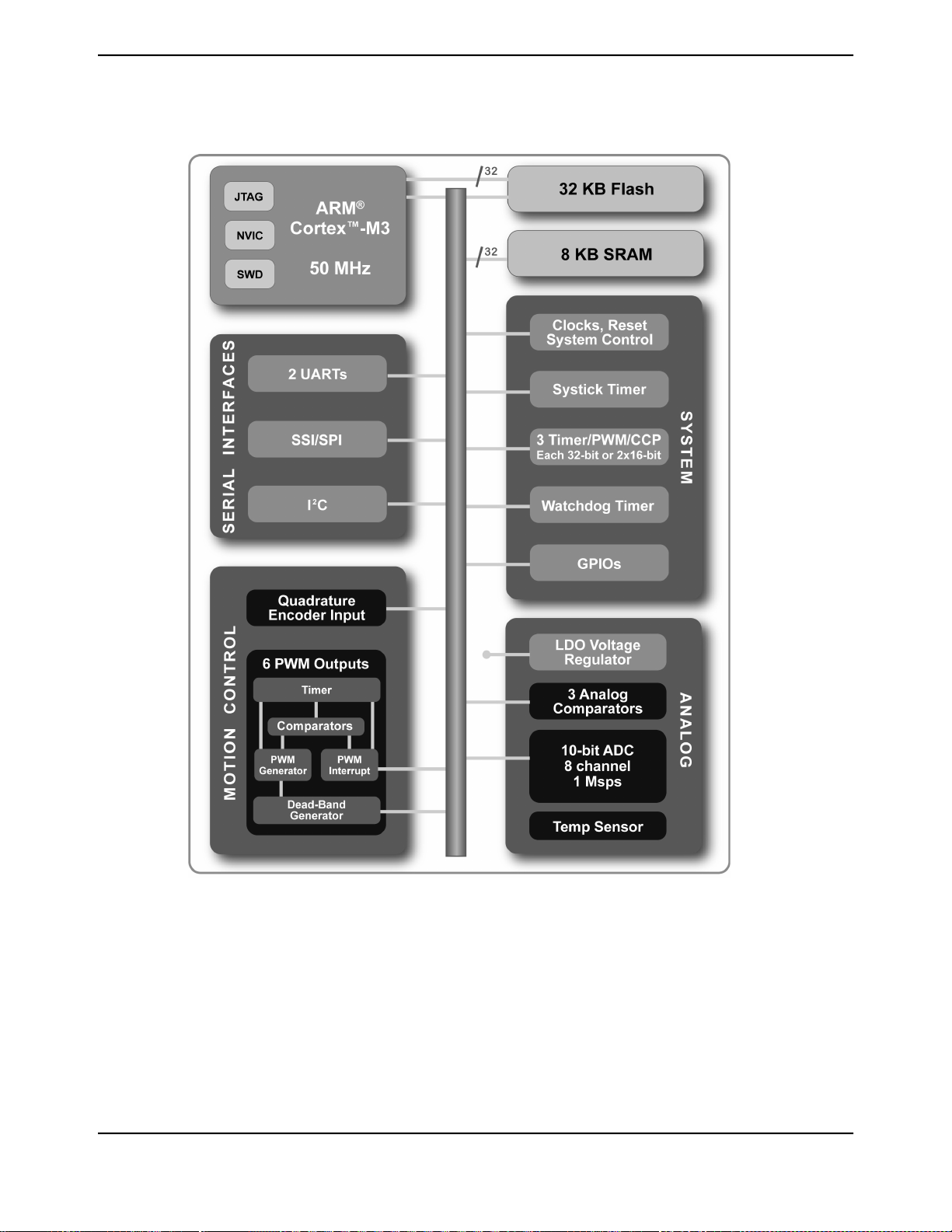
Figure 1-1. Stellaris®600 Series High-Level Block Diagram
LM3S617 Microcontroller
1.4 Functional Overview
The following sections provide an overview of the features of the LM3S617 microcontroller. The
page number in parenthesis indicates where that feature is discussed in detail. Ordering and support
information can be found in “Ordering and Contact Information” on page 420.
25November 29, 2007
Preliminary

Architectural Overview
1.4.1 ARM Cortex™-M3
1.4.1.1 Processor Core (see page 32)
All members of the Stellaris®product family, including the LM3S617 microcontroller, are designed
around an ARM Cortex™-M3 processor core. The ARM Cortex-M3 processor provides the core for
a high-performance, low-cost platform that meets the needs of minimal memory implementation,
reduced pin count, and low-power consumption, while delivering outstanding computational
performance and exceptional system response to interrupts.
“ARM Cortex-M3 Processor Core” on page 32 provides an overview of the ARM core; the core is
detailed in the ARM® Cortex™-M3 Technical Reference Manual.
1.4.1.2 System Timer (SysTick)
Cortex-M3 includes an integrated system timer, SysTick. SysTick provides a simple, 24-bit
clear-on-write, decrementing, wrap-on-zero counter with a flexible control mechanism. The counter
can be used in several different ways, for example:
■ An RTOS tick timer which fires at a programmable rate (for example, 100 Hz) and invokes a
SysTick routine.
■ A high-speed alarm timer using the system clock.
■ A variable rate alarm or signal timer—the duration is range-dependent on the reference clock
used and the dynamic range of the counter.
■ A simple counter. Software can use this to measure time to completion and time used.
■ An internal clock source control based on missing/meeting durations. The COUNTFLAG bit-field
in the control and status register can be used to determine if an action completed within a set
duration, as part of a dynamic clock management control loop.
1.4.1.3 Nested Vectored Interrupt Controller (NVIC)
The LM3S617 controller includes the ARM Nested Vectored Interrupt Controller (NVIC) on the ARM
Cortex-M3 core. The NVIC and Cortex-M3 prioritize and handle all exceptions. All exceptions are
handled in Handler Mode. The processor state is automatically stored to the stack on an exception,
and automatically restored from the stack at the end of the Interrupt Service Routine (ISR). The
vector is fetched in parallel to the state saving, which enables efficient interrupt entry. The processor
supports tail-chaining, which enables back-to-back interrupts to be performed without the overhead
of state saving and restoration. Software can set eight priority levels on 7 exceptions (system
handlers) and 25 interrupts.
“Interrupts” on page 40 provides an overview of the NVIC controller and the interrupt map. Exceptions
and interrupts are detailed in the ARM® Cortex™-M3 Technical Reference Manual.
1.4.2 Motor Control Peripherals
To enhance motor control, the LM3S617 controller features Pulse Width Modulation (PWM) outputs.
1.4.2.1 PWM
Pulse width modulation (PWM) is a powerful technique for digitally encoding analog signal levels.
High-resolution counters are used to generate a square wave, and the duty cycle of the square
wave is modulated to encode an analog signal. Typical applications include switching power supplies
and motor control.
November 29, 200726
Preliminary

On the LM3S617, PWM motion control functionality can be achieved through:
■ Dedicated, flexible motion control hardware using the PWM pins
■ The motion control features of the general-purpose timers using the CCP pins
PWM Pins (see page 343)
The LM3S617 PWM module consists of three PWM generator blocks and a control block. Each
PWM generator block contains one timer (16-bit down or up/down counter), two comparators, a
PWM signal generator, a dead-band generator, and an interrupt/ADC-trigger selector. The control
block determines the polarity of the PWM signals, and which signals are passed through to the pins.
Each PWM generator block produces two PWM signals that can either be independent signals or
a single pair of complementary signals with dead-band delays inserted. The output of the PWM
generation blocks are managed by the output control block before being passed to the device pins.
CCP Pins (see page 171)
The General-Purpose Timer Module's CCP (Capture Compare PWM) pins are software programmable
to support a simple PWM mode with a software-programmable output inversion of the PWM signal.
1.4.3 Analog Peripherals
LM3S617 Microcontroller
To handle analog signals, the LM3S617 microcontroller offers an Analog-to-Digital Converter (ADC).
For support of analog signals, the LM3S617 microcontroller offers one analog comparator.
1.4.3.1 ADC (see page 224)
An analog-to-digital converter (ADC) is a peripheral that converts a continuous analog voltage to a
discrete digital number.
The LM3S617 ADC module features 10-bit conversion resolution and supports six input channels,
plus an internal temperature sensor. Four buffered sample sequences allow rapid sampling of up
to eight analog input sources without controller intervention. Each sample sequence provides flexible
programming with fully configurable input source, trigger events, interrupt generation, and sequence
priority.
1.4.3.2 Analog Comparators (see page 332)
An analog comparator is a peripheral that compares two analog voltages, and provides a logical
output that signals the comparison result.
A comparator can compare a test voltage against any one of these voltages:
■ An individual external reference voltage
■ A shared single external reference voltage
■ A shared internal reference voltage
The comparator can provide its output to a device pin, acting as a replacement for an analog
comparator on the board, or it can be used to signal the application via interrupts or triggers to the
ADC to cause it to start capturing a sample sequence. The interrupt generation and ADC triggering
logic is separate. This means, for example, that an interrupt can be generated on a rising edge and
the ADC triggered on a falling edge.
27November 29, 2007
Preliminary

Architectural Overview
1.4.4 Serial Communications Peripherals
The LM3S617 controller supports both asynchronous and synchronous serial communications with:
■ Two fully programmable 16C550-type UARTs
■ One SSI module
1.4.4.1 UART (see page 257)
A Universal Asynchronous Receiver/Transmitter (UART) is an integrated circuit used for RS-232C
serial communications, containing a transmitter (parallel-to-serial converter) and a receiver
(serial-to-parallel converter), each clocked separately.
The LM3S617 controller includes two fully programmable 16C550-type UARTs that support data
transfer speeds up to 460.8 Kbps. (Although similar in functionality to a 16C550 UART, it is not
register-compatible.)
Separate 16x8 transmit (TX) and 16x12 receive (RX) FIFOs reduce CPU interrupt service loading.
The UART can generate individually masked interrupts from the RX, TX, modem status, and error
conditions. The module provides a single combined interrupt when any of the interrupts are asserted
and are unmasked.
1.4.4.2 SSI (see page 295)
Synchronous Serial Interface (SSI) is a four-wire bi-directional communications interface.
The LM3S617 controller includes one SSI module that provides the functionality for synchronous
serial communications with peripheral devices, and can be configured to use the Freescale SPI,
MICROWIRE, or TI synchronous serial interface frame formats. The size of the data frame is also
configurable, and can be set between 4 and 16 bits, inclusive.
The SSI module performs serial-to-parallel conversion on data received from a peripheral device,
and parallel-to-serial conversion on data transmitted to a peripheral device. The TX and RX paths
are buffered with internal FIFOs, allowing up to eight 16-bit values to be stored independently.
The SSI module can be configured as either a master or slave device. As a slave device, the SSI
module can also be configured to disable its output, which allows a master device to be coupled
with multiple slave devices.
The SSI module also includes a programmable bit rate clock divider and prescaler to generate the
output serial clock derived from the SSI module's input clock. Bit rates are generated based on the
input clock and the maximum bit rate is determined by the connected peripheral.
1.4.5 System Peripherals
1.4.5.1 Programmable GPIOs (see page 126)
General-purpose input/output (GPIO) pins offer flexibility for a variety of connections.
The Stellaris®GPIO module is composed of five physical GPIO blocks, each corresponding to an
individual GPIO port. The GPIO module is FiRM-compliant (compliant to the ARM Foundation IP
for Real-Time Microcontrollers specification) and supports 1-30 programmable input/output pins.
The number of GPIOs available depends on the peripherals being used (see “Signal Tables” on page
380 for the signals available to each GPIO pin).
The GPIO module features programmable interrupt generation as either edge-triggered or
level-sensitive on all pins, programmable control for GPIO pad configuration, and bit masking in
both read and write operations through address lines.
November 29, 200728
Preliminary

1.4.5.2 Three Programmable Timers (see page 165)
Programmable timers can be used to count or time external events that drive the Timer input pins.
The Stellaris®General-Purpose Timer Module (GPTM) contains three GPTM blocks. Each GPTM
block provides two 16-bit timers/counters that can be configured to operate independently as timers
or event counters, or configured to operate as one 32-bit timer or one 32-bit Real-Time Clock (RTC).
Timers can also be used to trigger analog-to-digital (ADC) conversions.
When configured in 32-bit mode, a timer can run as a Real-Time Clock (RTC), one-shot timer or
periodic timer. When in 16-bit mode, a timer can run as a one-shot timer or periodic timer, and can
extend its precision by using an 8-bit prescaler. A 16-bit timer can also be configured for event
capture or Pulse Width Modulation (PWM) generation.
1.4.5.3 Watchdog Timer (see page 201)
A watchdog timer can generate nonmaskable interrupts (NMIs) or a reset when a time-out value is
reached. The watchdog timer is used to regain control when a system has failed due to a software
error or to the failure of an external device to respond in the expected way.
The Stellaris®Watchdog Timer module consists of a 32-bit down counter, a programmable load
register, interrupt generation logic, and a locking register.
LM3S617 Microcontroller
The Watchdog Timer can be configured to generate an interrupt to the controller on its first time-out,
and to generate a reset signal on its second time-out. Once the Watchdog Timer has been configured,
the lock register can be written to prevent the timer configuration from being inadvertently altered.
1.4.6 Memory Peripherals
The LM3S617 controller offers both single-cycle SRAM and single-cycle Flash memory.
1.4.6.1 SRAM (see page 110)
The LM3S617 static random access memory (SRAM) controller supports 8 KB SRAM. The internal
SRAM of the Stellaris®devices is located at offset 0x0000.0000 of the device memory map. To
reduce the number of time-consuming read-modify-write (RMW) operations, ARM has introduced
bit-banding technology in the new Cortex-M3 processor. With a bit-band-enabled processor, certain
regions in the memory map (SRAM and peripheral space) can use address aliases to access
individual bits in a single, atomic operation.
1.4.6.2 Flash (see page 111)
The LM3S617 Flash controller supports 32 KB of flash memory. The flash is organized as a set of
1-KB blocks that can be individually erased. Erasing a block causes the entire contents of the block
to be reset to all 1s. These blocks are paired into a set of 2-KB blocks that can be individually
protected. The blocks can be marked as read-only or execute-only, providing different levels of code
protection. Read-only blocks cannot be erased or programmed, protecting the contents of those
blocks from being modified. Execute-only blocks cannot be erased or programmed, and can only
be read by the controller instruction fetch mechanism, protecting the contents of those blocks from
being read by either the controller or by a debugger.
1.4.7 Additional Features
1.4.7.1 Memory Map (see page 38)
A memory map lists the location of instructions and data in memory. The memory map for the
LM3S617 controller can be found in “Memory Map” on page 38. Register addresses are given as
a hexadecimal increment, relative to the module's base address as shown in the memory map.
29November 29, 2007
Preliminary

Architectural Overview
The ARM® Cortex™-M3 Technical Reference Manual provides further information on the memory
map.
1.4.7.2 JTAG TAP Controller (see page 42)
The Joint Test Action Group (JTAG) port provides a standardized serial interface for controlling the
Test Access Port (TAP) and associated test logic. The TAP, JTAG instruction register, and JTAG
data registers can be used to test the interconnects of assembled printed circuit boards, obtain
manufacturing information on the components, and observe and/or control the inputs and outputs
of the controller during normal operation. The JTAG port provides a high degree of testability and
chip-level access at a low cost.
The JTAG port is comprised of the standard five pins: TRST, TCK, TMS, TDI, and TDO. Data is
transmitted serially into the controller on TDI and out of the controller on TDO. The interpretation of
this data is dependent on the current state of the TAP controller. For detailed information on the
operation of the JTAG port and TAP controller, please refer to the IEEE Standard 1149.1-Test
Access Port and Boundary-Scan Architecture.
The Luminary Micro JTAG controller works with the ARM JTAG controller built into the Cortex-M3
core. This is implemented by multiplexing the TDO outputs from both JTAG controllers. ARM JTAG
instructions select the ARM TDO output while Luminary Micro JTAG instructions select the Luminary
Micro TDO outputs. The multiplexer is controlled by the Luminary Micro JTAG controller, which has
comprehensive programming for the ARM, Luminary Micro, and unimplemented JTAG instructions.
1.4.7.3 System Control and Clocks (see page 52)
System control determines the overall operation of the device. It provides information about the
device, controls the clocking of the device and individual peripherals, and handles reset detection
and reporting.
1.4.8 Hardware Details
Details on the pins and package can be found in the following sections:
■ “Pin Diagram” on page 379
■ “Signal Tables” on page 380
■ “Operating Characteristics” on page 387
■ “Electrical Characteristics” on page 388
■ “Package Information” on page 398
Preliminary
November 29, 200730
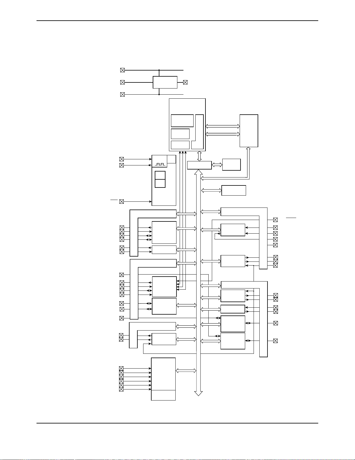
Flash
SRAM
APB Bridge
ICode
DCode
GND
VDD_3.3V
LDO VDD_2.5V
LDO
System
Control
& Clocks
OSC0
OSC1
RST
PLL
Watchdog
Timer
POR
BOR
IOSC
Debug
ARM Cortex-M3
NVIC
CM3Core
Bus
UART0
PA1/U0Tx
PA0/U0Rx
GPIO Port A
SSI
PA3/SSIFss
PA2/SSIClk
PA5/SSITx
PA4/SSIRx
(8 KB)
(32 KB)
(50 MHz)
GPIO Port B
GPIO Port C
PC1/TMS/SWDIO
PC0/TCK/SWCLK
PC3/TDO/SWO
PC2/TDI
PB3/Fault
PB2
PB5/C0o
PB4/C0-
PB6/C0+
GP Timer2
GP Timer0
PB7/TRST
Analog
Comparator
GP Timer1
GPIO Port D
ADC
Temperature
Sensor
GPIO Port E
ADC4
ADC5
ADC2
ADC0
ADC1
PE0/PWM4
PE1/PWM5
PWM0
PD0/PWM0
PD1/PWM1
PD4/CCP0
PD5/CCP2
PD2/U1Rx
PD3/U1Tx
PWM1
PB1/PWM3
PB0/PWM2
ADC3
PC6/CCP3
PC7/CCP4
PC5/CCP1
PC4/CCP5
LM3S617
JTAG
SWD/SWO
PWM2
Peripheral Bus
UART1
LM3S617 Microcontroller
1.4.9 System Block Diagram
Figure 1-2. LM3S617 Controller System-Level Block Diagram
31November 29, 2007
Preliminary

ARM Cortex-M3 Processor Core
2 ARM Cortex-M3 Processor Core
The ARM Cortex-M3 processor provides the core for a high-performance, low-cost platform that
meets the needs of minimal memory implementation, reduced pin count, and low power consumption,
while delivering outstanding computational performance and exceptional system response to
interrupts. Features include:
■ Compact core.
■ Thumb-2 instruction set, delivering the high-performance expected of an ARM core in the memory
size usually associated with 8- and 16-bit devices; typically in the range of a few kilobytes of
memory for microcontroller class applications.
■ Rapid application execution through Harvard architecture characterized by separate buses for
instruction and data.
■ Exceptional interrupt handling, by implementing the register manipulations required for handling
an interrupt in hardware.
■ Memory protection unit (MPU) to provide a privileged mode of operation for complex applications.
■ Migration from the ARM7™ processor family for better performance and power efficiency.
■ Full-featured debug solution with a:
– Serial Wire JTAG Debug Port (SWJ-DP)
– Flash Patch and Breakpoint (FPB) unit for implementing breakpoints
– Data Watchpoint and Trigger (DWT) unit for implementing watchpoints, trigger resources,
and system profiling
– Instrumentation Trace Macrocell (ITM) for support of printf style debugging
– Trace Port Interface Unit (TPIU) for bridging to a Trace Port Analyzer
The Stellaris®family of microcontrollers builds on this core to bring high-performance 32-bit computing
to cost-sensitive embedded microcontroller applications, such as factory automation and control,
industrial control power devices, building and home automation, and stepper motors.
For more information on the ARM Cortex-M3 processor core, see the ARM® Cortex™-M3 Technical
Reference Manual. For information on SWJ-DP, see the ARM® CoreSight Technical Reference
Manual.
Preliminary
November 29, 200732

2.1 Block Diagram
Private Peripheral
Bus
(internal)
Data
Watchpoint
and Trace
Interrupts
Debug
Sleep
Instrumentation
Trace Macrocell
Trace
Port
Interface
Unit
CM3 Core
Instructions Data
Flash
Patch and
Breakpoint
Memory
Protection
Unit
Adv. High-
Perf. Bus
Access Port
Nested
Vectored
Interrupt
Controller
Serial Wire JTAG
Debug Port
Bus
Matrix
Adv. Peripheral
Bus
I-code bus
D-code bus
System bus
ROM
Table
Private
Peripheral
Bus
(external)
Serial
Wire
Output
Trace
Port
(SWO)
ARM
Cortex-M3
Figure 2-1. CPU Block Diagram
LM3S617 Microcontroller
2.2 Functional Description
2.2.1 Serial Wire and JTAG Debug
Important:
Luminary Micro has implemented the ARM Cortex-M3 core as shown in Figure 2-1 on page 33. As
noted in the ARM® Cortex™-M3 Technical Reference Manual, several Cortex-M3 components are
flexible in their implementation: SW/JTAG-DP, ETM, TPIU, the ROM table, the MPU, and the Nested
Vectored Interrupt Controller (NVIC). Each of these is addressed in the sections that follow.
Luminary Micro has replaced the ARM SW-DP and JTAG-DP with the ARM CoreSight™-compliant
Serial Wire JTAG Debug Port (SWJ-DP) interface. This means Chapter 12, “Debug Port,” of the
ARM® Cortex™-M3 Technical Reference Manual does not apply to Stellaris®devices.
The SWJ-DP interface combines the SWD and JTAG debug ports into one module. See the
CoreSight™ Design Kit Technical Reference Manual for details on SWJ-DP.
The ARM® Cortex™-M3 Technical Reference Manual describes all the features of an
ARM Cortex-M3 in detail. However, these features differ based on the implementation.
This section describes the Stellaris®implementation.
Preliminary
33November 29, 2007
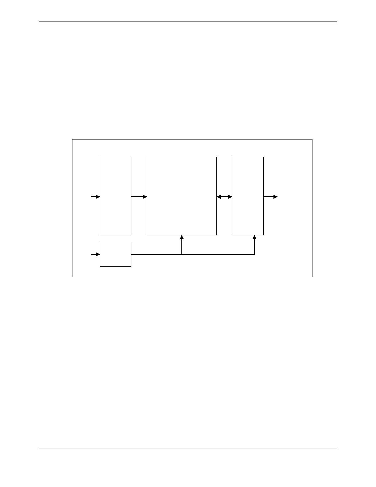
ATB
Interface
Asynchronous FIFO
APB
Interface
Trace Out
(serializer)
Debug
ATB
Slave
Port
APB
Slave
Port
Serial Wire
Trace Port
(SWO)
ARM Cortex-M3 Processor Core
2.2.2 Embedded Trace Macrocell (ETM)
ETM was not implemented in the Stellaris®devices. This means Chapters 15 and 16 of the ARM®
Cortex™-M3 Technical Reference Manual can be ignored.
2.2.3 Trace Port Interface Unit (TPIU)
The TPIU acts as a bridge between the Cortex-M3 trace data from the ITM, and an off-chip Trace
Port Analyzer. The Stellaris®devices have implemented TPIU as shown in Figure 2-2 on page 34.
This is similar to the non-ETM version described in the ARM® Cortex™-M3 Technical Reference
Manual, however, SWJ-DP only provides SWV output for the TPIU.
Figure 2-2. TPIU Block Diagram
2.2.4 ROM Table
The default ROM table was implemented as described in the ARM® Cortex™-M3 Technical
Reference Manual.
2.2.5 Memory Protection Unit (MPU)
The Memory Protection Unit (MPU) is included on the LM3S617 controller and supports the standard
ARMv7 Protected Memory System Architecture (PMSA) model. The MPU provides full support for
protection regions, overlapping protection regions, access permissions, and exporting memory
attributes to the system.
2.2.6 Nested Vectored Interrupt Controller (NVIC)
The Nested Vectored Interrupt Controller (NVIC):
■ Facilitates low-latency exception and interrupt handling
■ Controls power management
■ Implements system control registers
Preliminary
November 29, 200734

The NVIC supports up to 240 dynamically reprioritizable interrupts each with up to 256 levels of
priority. The NVIC and the processor core interface are closely coupled, which enables low latency
interrupt processing and efficient processing of late arriving interrupts. The NVIC maintains knowledge
of the stacked (nested) interrupts to enable tail-chaining of interrupts.
You can only fully access the NVIC from privileged mode, but you can pend interrupts in user-mode
if you enable the Configuration Control Register (see the ARM® Cortex™-M3 Technical Reference
Manual). Any other user-mode access causes a bus fault.
All NVIC registers are accessible using byte, halfword, and word unless otherwise stated.
All NVIC registers and system debug registers are little endian regardless of the endianness state
of the processor.
2.2.6.1 Interrupts
The ARM® Cortex™-M3 Technical Reference Manual describes the maximum number of interrupts
and interrupt priorities. The LM3S617 microcontroller supports 25 interrupts with eight priority levels.
2.2.6.2 System Timer (SysTick)
Cortex-M3 includes an integrated system timer, SysTick. SysTick provides a simple, 24-bit
clear-on-write, decrementing, wrap-on-zero counter with a flexible control mechanism. The counter
can be used in several different ways, for example:
LM3S617 Microcontroller
■ An RTOS tick timer which fires at a programmable rate (for example, 100 Hz) and invokes a
SysTick routine.
■ A high-speed alarm timer using the system clock.
■ A variable rate alarm or signal timer—the duration is range-dependent on the reference clock
used and the dynamic range of the counter.
■ A simple counter. Software can use this to measure time to completion and time used.
■ An internal clock source control based on missing/meeting durations. The COUNTFLAG bit-field
in the control and status register can be used to determine if an action completed within a set
duration, as part of a dynamic clock management control loop.
Functional Description
The timer consists of three registers:
■ A control and status counter to configure its clock, enable the counter, enable the SysTick
interrupt, and determine counter status.
■ The reload value for the counter, used to provide the counter's wrap value.
■ The current value of the counter.
A fourth register, the SysTick Calibration Value Register, is not implemented in the Stellaris®devices.
When enabled, the timer counts down from the reload value to zero, reloads (wraps) to the value
in the SysTick Reload Value register on the next clock edge, then decrements on subsequent clocks.
Writing a value of zero to the Reload Value register disables the counter on the next wrap. When
the counter reaches zero, the COUNTFLAG status bit is set. The COUNTFLAG bit clears on reads.
35November 29, 2007
Preliminary

ARM Cortex-M3 Processor Core
Writing to the Current Value register clears the register and the COUNTFLAG status bit. The write
does not trigger the SysTick exception logic. On a read, the current value is the value of the register
at the time the register is accessed.
If the core is in debug state (halted), the counter will not decrement. The timer is clocked with respect
to a reference clock. The reference clock can be the core clock or an external clock source.
SysTick Control and Status Register
Use the SysTick Control and Status Register to enable the SysTick features. The reset is
0x0000.0000.
DescriptionResetTypeNameBit/Field
Software should not rely on the value of a reserved bit. To provide compatibility with
0ROreserved31:17
future products, the value of a reserved bit should be preserved across a
read-modify-write operation.
Returns 1 if timer counted to 0 since last time this was read. Clears on read by
0R/WCOUNTFLAG16
application. If read by the debugger using the DAP, this bit is cleared on read-only
if the MasterType bit in the AHB-AP Control Register is set to 0. Otherwise, the
COUNTFLAG bit is not changed by the debugger read.
Software should not rely on the value of a reserved bit. To provide compatibility with
0ROreserved15:3
future products, the value of a reserved bit should be preserved across a
read-modify-write operation.
0 = external reference clock. (Not implemented for Stellaris microcontrollers.)
0R/WCLKSOURCE2
1 = core clock.
If no reference clock is provided, it is held at 1 and so gives the same time as the
core clock. The core clock must be at least 2.5 times faster than the reference clock.
If it is not, the count values are unpredictable.
1 = counting down to 0 pends the SysTick handler.
0R/WTICKINT1
0 = counting down to 0 does not pend the SysTick handler. Software can use the
COUNTFLAG to determine if ever counted to 0.
1 = counter operates in a multi-shot way. That is, counter loads with the Reload
0R/WENABLE0
value and then begins counting down. On reaching 0, it sets the COUNTFLAG to
1 and optionally pends the SysTick handler, based on TICKINT. It then loads the
Reload value again, and begins counting.
0 = counter disabled.
SysTick Reload Value Register
Use the SysTick Reload Value Register to specify the start value to load into the current value
register when the counter reaches 0. It can be any value between 1 and 0x00FF.FFFF. A start value
of 0 is possible, but has no effect because the SysTick interrupt and COUNTFLAG are activated
when counting from 1 to 0.
Therefore, as a multi-shot timer, repeated over and over, it fires every N+1 clock pulse, where N is
any value from 1 to 0x00FF.FFFF. So, if the tick interrupt is required every 100 clock pulses, 99
must be written into the RELOAD. If a new value is written on each tick interrupt, so treated as single
shot, then the actual count down must be written. For example, if a tick is next required after 400
clock pulses, 400 must be written into the RELOAD.
DescriptionResetTypeNameBit/Field
Software should not rely on the value of a reserved bit. To provide compatibility with
0ROreserved31:24
future products, the value of a reserved bit should be preserved across a read-modify-write
operation.
November 29, 200736
Preliminary

LM3S617 Microcontroller
DescriptionResetTypeNameBit/Field
Value to load into the SysTick Current Value Register when the counter reaches 0.-W1CRELOAD23:0
SysTick Current Value Register
Use the SysTick Current Value Register to find the current value in the register.
DescriptionResetTypeNameBit/Field
Software should not rely on the value of a reserved bit. To provide compatibility with
0ROreserved31:24
future products, the value of a reserved bit should be preserved across a
read-modify-write operation.
Current value at the time the register is accessed. No read-modify-write protection is
-W1CCURRENT23:0
provided, so change with care.
This register is write-clear. Writing to it with any value clears the register to 0. Clearing
this register also clears the COUNTFLAG bit of the SysTick Control and Status Register.
SysTick Calibration Value Register
The SysTick Calibration Value register is not implemented.
Preliminary
37November 29, 2007

Memory Map
3 Memory Map
The memory map for the LM3S617 controller is provided in Table 3-1 on page 38.
In this manual, register addresses are given as a hexadecimal increment, relative to the module’s
base address as shown in the memory map. See also Chapter 4, “Memory Map” in the ARM®
Cortex™-M3 Technical Reference Manual.
Important: In Table 3-1 on page 38, addresses not listed are reserved.
Table 3-1. Memory Map
Memory
FiRM Peripherals
Peripherals
Private Peripheral Bus
a
DescriptionEndStart
0x0000.7FFF0x0000.0000
0x2000.1FFF0x2000.0000
b
c
For details on
registers, see
page ...
115On-chip flash
115Bit-banded on-chip SRAM
-Reserved0x200F.FFFF0x2010.0000
110Bit-band alias of 0x2000.0000 through 0x200F.FFFF0x22003.FFFF0x2200.0000
-Reserved0x23FF.FFFF0x2204.0000
203Watchdog timer0x4000.0FFF0x4000.0000
133GPIO Port A0x4000.4FFF0x4000.4000
133GPIO Port B0x4000.5FFF0x4000.5000
133GPIO Port C0x4000.6FFF0x4000.6000
133GPIO Port D0x4000.7FFF0x4000.7000
306SSI00x4000.8FFF0x4000.8000
263UART00x4000.CFFF0x4000.C000
263UART10x4000.DFFF0x4000.D000
133GPIO Port E0x4002.7FFF0x4002.4000
350PWM0x4002.8FFF0x4002.8000
176Timer00x4003.0FFF0x4003.0000
176Timer10x4003.1FFF0x4003.1000
176Timer20x4003.2FFF0x4003.2000
230ADC0x4003.8FFF0x4003.8000
332Analog Comparators0x4003.CFFF0x4003.C000
115Flash control0x400F.DFFF0x400F.D000
60System control0x400F.FFFF0x400F.E000
-Bit-banded alias of 0x4000.0000 through 0x400F.FFFF0x43FF.FFFF0x4200.0000
Preliminary
November 29, 200738
LM3S617 Microcontroller
a. All reserved space returns a bus fault when read or written.
b. The unavailable flash will bus fault throughout this range.
c. The unavailable SRAM will bus fault throughout this range.
DescriptionEndStart
Instrumentation Trace Macrocell (ITM)0xE000.0FFF0xE000.0000
Data Watchpoint and Trace (DWT)0xE000.1FFF0xE000.1000
Flash Patch and Breakpoint (FPB)0xE000.2FFF0xE000.2000
Reserved0xE000.DFFF0xE000.3000
Nested Vectored Interrupt Controller (NVIC)0xE000.EFFF0xE000.E000
Reserved0xE003.FFFF0xE000.F000
Trace Port Interface Unit (TPIU)0xE004.0FFF0xE004.0000
For details on
registers, see
page ...
ARM®
Cortex™-M3
Technical
Reference
Manual
-Reserved0xE004.1FFF0xE004.1000
-Reserved0xE00F.FFFF0xE004.2000
-Reserved for vendor peripherals0xFFFF.FFFF0xE010.0000
Preliminary
39November 29, 2007

Interrupts
4 Interrupts
The ARM Cortex-M3 processor and the Nested Vectored Interrupt Controller (NVIC) prioritize and
handle all exceptions. All exceptions are handled in Handler Mode. The processor state is
automatically stored to the stack on an exception, and automatically restored from the stack at the
end of the Interrupt Service Routine (ISR). The vector is fetched in parallel to the state saving, which
enables efficient interrupt entry. The processor supports tail-chaining, which enables back-to-back
interrupts to be performed without the overhead of state saving and restoration.
Table 4-1 on page 40 lists all the exceptions. Software can set eight priority levels on seven of these
exceptions (system handlers) as well as on 25 interrupts (listed in Table 4-2 on page 41).
Priorities on the system handlers are set with the NVIC System Handler Priority registers. Interrupts
are enabled through the NVIC Interrupt Set Enable register and prioritized with the NVIC Interrupt
Priority registers. You can also group priorities by splitting priority levels into pre-emption priorities
and subpriorities. All the interrupt registers are described in Chapter 8, “Nested Vectored Interrupt
Controller” in the ARM® Cortex™-M3 Technical Reference Manual.
Internally, the highest user-settable priority (0) is treated as fourth priority, after a Reset, NMI, and
a Hard Fault. Note that 0 is the default priority for all the settable priorities.
If you assign the same priority level to two or more interrupts, their hardware priority (the lower the
position number) determines the order in which the processor activates them. For example, if both
GPIO Port A and GPIO Port B are priority level 1, then GPIO Port A has higher priority.
See Chapter 5, “Exceptions” and Chapter 8, “Nested Vectored Interrupt Controller” in the ARM®
Cortex™-M3 Technical Reference Manual for more information on exceptions and interrupts.
Note: In Table 4-2 on page 41 interrupts not listed are reserved.
Table 4-1. Exception Types
a
PositionException Type
-3 (highest)1Reset
Interrupt (NMI)
settable4Memory Management
settable5Bus Fault
settable6Usage Fault
DescriptionPriority
Stack top is loaded from first entry of vector table on reset.-0-
Invoked on power up and warm reset. On first instruction, drops to lowest
priority (and then is called the base level of activation). This is
asynchronous.
Cannot be stopped or preempted by any exception but reset. This is
-22Non-Maskable
asynchronous.
An NMI is only producible by software, using the NVIC Interrupt Control
State register.
All classes of Fault, when the fault cannot activate due to priority or the
-13Hard Fault
configurable fault handler has been disabled. This is synchronous.
MPU mismatch, including access violation and no match. This is
synchronous.
The priority of this exception can be changed.
Pre-fetch fault, memory access fault, and other address/memory related
faults. This is synchronous when precise and asynchronous when
imprecise.
You can enable or disable this fault.
Usage fault, such as undefined instruction executed or illegal state
transition attempt. This is synchronous.
Reserved.-7-10-
System service call with SVC instruction. This is synchronous.settable11SVCall
Preliminary
November 29, 200740
a
PositionException Type
settable12Debug Monitor
settable14PendSV
Interrupts
above
a. 0 is the default priority for all the settable priorities.
settable16 and
DescriptionPriority
Debug monitor (when not halting). This is synchronous, but only active
when enabled. It does not activate if lower priority than the current
activation.
Reserved.-13-
Pendable request for system service. This is asynchronous and only
pended by software.
System tick timer has fired. This is asynchronous.settable15SysTick
Asserted from outside the ARM Cortex-M3 core and fed through the NVIC
(prioritized). These are all asynchronous. Table 4-2 on page 41 lists the
interrupts on the LM3S617 controller.
Table 4-2. Interrupts
DescriptionInterrupt (Bit in Interrupt Registers)
GPIO Port A0
GPIO Port B1
GPIO Port C2
GPIO Port D3
GPIO Port E4
UART05
UART16
SSI07
PWM Generator 010
PWM Generator 111
PWM Generator 212
ADC Sequence 014
ADC Sequence 115
ADC Sequence 216
ADC Sequence 317
Watchdog timer18
Timer0 A19
Timer0 B20
Timer1 A21
Timer1 B22
Timer2 A23
Timer2 B24
Analog Comparator 025
System Control28
Flash Control29
LM3S617 Microcontroller
Preliminary
41November 29, 2007

JTAG Interface
5 JTAG Interface
The Joint Test Action Group (JTAG) port is an IEEE standard that defines a Test Access Port and
Boundary Scan Architecture for digital integrated circuits and provides a standardized serial interface
for controlling the associated test logic. The TAP, Instruction Register (IR), and Data Registers (DR)
can be used to test the interconnections of assembled printed circuit boards and obtain manufacturing
information on the components. The JTAG Port also provides a means of accessing and controlling
design-for-test features such as I/O pin observation and control, scan testing, and debugging.
The JTAG port is comprised of the standard five pins: TRST, TCK, TMS, TDI, and TDO. Data is
transmitted serially into the controller on TDI and out of the controller on TDO. The interpretation of
this data is dependent on the current state of the TAP controller. For detailed information on the
operation of the JTAG port and TAP controller, please refer to the IEEE Standard 1149.1-Test
Access Port and Boundary-Scan Architecture.
The Luminary Micro JTAG controller works with the ARM JTAG controller built into the Cortex-M3
core. This is implemented by multiplexing the TDO outputs from both JTAG controllers. ARM JTAG
instructions select the ARM TDO output while Luminary Micro JTAG instructions select the Luminary
Micro TDO outputs. The multiplexer is controlled by the Luminary Micro JTAG controller, which has
comprehensive programming for the ARM, Luminary Micro, and unimplemented JTAG instructions.
The JTAG module has the following features:
■ IEEE 1149.1-1990 compatible Test Access Port (TAP) controller
■ Four-bit Instruction Register (IR) chain for storing JTAG instructions
■ IEEE standard instructions:
– BYPASS instruction
– IDCODE instruction
– SAMPLE/PRELOAD instruction
– EXTEST instruction
– INTEST instruction
■ ARM additional instructions:
– APACC instruction
– DPACC instruction
– ABORT instruction
■ Integrated ARM Serial Wire Debug (SWD)
See the ARM® Cortex™-M3 Technical Reference Manual for more information on the ARM JTAG
controller.
November 29, 200742
Preliminary
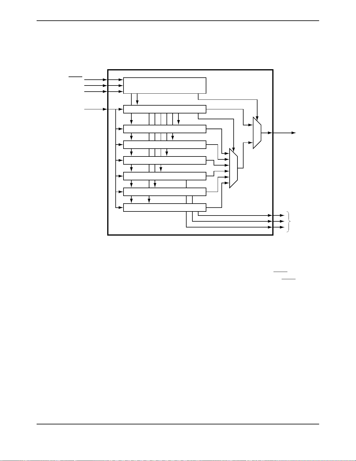
5.1 Block Diagram
Instruction Register(IR)
TAP Controller
BYPASS Data Register
Boundary Scan Data Register
IDCODE Data Register
ABORT Data Register
DPACC Data Register
APACC Data Register
TRST
TCK
TMS
TDI
TDO
Cortex-M3
Debug
Port
Figure 5-1. JTAG Module Block Diagram
LM3S617 Microcontroller
5.2 Functional Description
A high-level conceptual drawing of the JTAG module is shown in Figure 5-1 on page 43. The JTAG
module is composed of the Test Access Port (TAP) controller and serial shift chains with parallel
update registers. The TAP controller is a simple state machine controlled by the TRST, TCK and
TMS inputs. The current state of the TAP controller depends on the current value of TRST and the
sequence of values captured on TMS at the rising edge of TCK. The TAP controller determines when
the serial shift chains capture new data, shift data from TDI towards TDO, and update the parallel
load registers. The current state of the TAP controller also determines whether the Instruction
Register (IR) chain or one of the Data Register (DR) chains is being accessed.
The serial shift chains with parallel load registers are comprised of a single Instruction Register (IR)
chain and multiple Data Register (DR) chains. The current instruction loaded in the parallel load
register determines which DR chain is captured, shifted, or updated during the sequencing of the
TAP controller.
Some instructions, like EXTEST and INTEST, operate on data currently in a DR chain and do not
capture, shift, or update any of the chains. Instructions that are not implemented decode to the
BYPASS instruction to ensure that the serial path between TDI and TDO is always connected (see
Table 5-2 on page 48 for a list of implemented instructions).
See “JTAG and Boundary Scan” on page 393 for JTAG timing diagrams.
Preliminary
43November 29, 2007

JTAG Interface
5.2.1 JTAG Interface Pins
The JTAG interface consists of five standard pins: TRST, TCK, TMS, TDI, and TDO. These pins and
their associated reset state are given in Table 5-1 on page 44. Detailed information on each pin
follows.
Table 5-1. JTAG Port Pins Reset State
5.2.1.1 Test Reset Input (TRST)
The TRST pin is an asynchronous active Low input signal for initializing and resetting the JTAG TAP
controller and associated JTAG circuitry. When TRST is asserted, the TAP controller resets to the
Test-Logic-Reset state and remains there while TRST is asserted. When the TAP controller enters
the Test-Logic-Reset state, the JTAG Instruction Register (IR) resets to the default instruction,
IDCODE.
Drive ValueDrive StrengthInternal Pull-DownInternal Pull-UpData DirectionPin Name
N/AN/ADisabledEnabledInputTRST
N/AN/ADisabledEnabledInputTCK
N/AN/ADisabledEnabledInputTMS
N/AN/ADisabledEnabledInputTDI
High-Z2-mA driverDisabledEnabledOutputTDO
By default, the internal pull-up resistor on the TRST pin is enabled after reset. Changes to the pull-up
resistor settings on GPIO Port B should ensure that the internal pull-up resistor remains enabled
on PB7/TRST; otherwise JTAG communication could be lost.
5.2.1.2 Test Clock Input (TCK)
The TCK pin is the clock for the JTAG module. This clock is provided so the test logic can operate
independently of any other system clocks. In addition, it ensures that multiple JTAG TAP controllers
that are daisy-chained together can synchronously communicate serial test data between
components. During normal operation, TCK is driven by a free-running clock with a nominal 50%
duty cycle. When necessary, TCK can be stopped at 0 or 1 for extended periods of time. While TCK
is stopped at 0 or 1, the state of the TAP controller does not change and data in the JTAG Instruction
and Data Registers is not lost.
By default, the internal pull-up resistor on the TCK pin is enabled after reset. This assures that no
clocking occurs if the pin is not driven from an external source. The internal pull-up and pull-down
resistors can be turned off to save internal power as long as the TCK pin is constantly being driven
by an external source.
5.2.1.3 Test Mode Select (TMS)
The TMS pin selects the next state of the JTAG TAP controller. TMS is sampled on the rising edge
of TCK. Depending on the current TAP state and the sampled value of TMS, the next state is entered.
Because the TMS pin is sampled on the rising edge of TCK, the IEEE Standard 1149.1 expects the
value on TMS to change on the falling edge of TCK.
Holding TMS high for five consecutive TCK cycles drives the TAP controller state machine to the
Test-Logic-Reset state. When the TAP controller enters the Test-Logic-Reset state, the JTAG
Instruction Register (IR) resets to the default instruction, IDCODE. Therefore, this sequence can
be used as a reset mechanism, similar to asserting TRST. The JTAG Test Access Port state machine
can be seen in its entirety in Figure 5-2 on page 46.
Preliminary
November 29, 200744

By default, the internal pull-up resistor on the TMS pin is enabled after reset. Changes to the pull-up
resistor settings on GPIO Port C should ensure that the internal pull-up resistor remains enabled
on PC1/TMS; otherwise JTAG communication could be lost.
5.2.1.4 Test Data Input (TDI)
The TDI pin provides a stream of serial information to the IR chain and the DR chains. TDI is
sampled on the rising edge of TCK and, depending on the current TAP state and the current
instruction, presents this data to the proper shift register chain. Because the TDI pin is sampled on
the rising edge of TCK, the IEEE Standard 1149.1 expects the value on TDI to change on the falling
edge of TCK.
By default, the internal pull-up resistor on the TDI pin is enabled after reset. Changes to the pull-up
resistor settings on GPIO Port C should ensure that the internal pull-up resistor remains enabled
on PC2/TDI; otherwise JTAG communication could be lost.
5.2.1.5 Test Data Output (TDO)
The TDO pin provides an output stream of serial information from the IR chain or the DR chains.
The value of TDO depends on the current TAP state, the current instruction, and the data in the
chain being accessed. In order to save power when the JTAG port is not being used, the TDO pin
is placed in an inactive drive state when not actively shifting out data. Because TDO can be connected
to the TDI of another controller in a daisy-chain configuration, the IEEE Standard 1149.1 expects
the value on TDO to change on the falling edge of TCK.
LM3S617 Microcontroller
By default, the internal pull-up resistor on the TDO pin is enabled after reset. This assures that the
pin remains at a constant logic level when the JTAG port is not being used. The internal pull-up and
pull-down resistors can be turned off to save internal power if a High-Z output value is acceptable
during certain TAP controller states.
5.2.2 JTAG TAP Controller
The JTAG TAP controller state machine is shown in Figure 5-2 on page 46. The TAP controller
state machine is reset to the Test-Logic-Reset state on the assertion of a Power-On-Reset (POR)
or the assertion of TRST. Asserting the correct sequence on the TMS pin allows the JTAG module
to shift in new instructions, shift in data, or idle during extended testing sequences. For detailed
information on the function of the TAP controller and the operations that occur in each state, please
refer to IEEE Standard 1149.1.
Preliminary
45November 29, 2007

Test Logic Reset
Run Test Idle Select DR Scan Select IR Scan
Capture DR Capture IR
Shift DR Shift IR
Exit 1 DR Exit 1 IR
Exit 2 DR Exit 2 IR
Pause DR Pause IR
Update DR Update IR
1 11
1 1
1
1 1
1 1
1 1
1 1
1 10 0
00
00
0 0
0 0
0 0
00
0
0
JTAG Interface
Figure 5-2. Test Access Port State Machine
5.2.3 Shift Registers
The Shift Registers consist of a serial shift register chain and a parallel load register. The serial shift
register chain samples specific information during the TAP controller’s CAPTURE states and allows
this information to be shifted out of TDO during the TAP controller’s SHIFT states. While the sampled
data is being shifted out of the chain on TDO, new data is being shifted into the serial shift register
on TDI. This new data is stored in the parallel load register during the TAP controller’s UPDATE
states. Each of the shift registers is discussed in detail in “Register Descriptions” on page 48.
5.2.4 Operational Considerations
There are certain operational considerations when using the JTAG module. Because the JTAG pins
can be programmed to be GPIOs, board configuration and reset conditions on these pins must be
considered. In addition, because the JTAG module has integrated ARM Serial Wire Debug, the
method for switching between these two operational modes is described below.
Preliminary
November 29, 200746

5.2.4.1 GPIO Functionality
When the controller is reset with either a POR or RST, the JTAG port pins default to their JTAG
configurations. The default configuration includes enabling the pull-up resistors (setting GPIOPUR
to 1 for PB7 and PC[3:0]) and enabling the alternate hardware function (setting GPIOAFSEL to
1 for PB7 and PC[3:0]) on the JTAG pins.
It is possible for software to configure these pins as GPIOs after reset by writing 0s to PB7 and
PC[3:0] in the GPIOAFSEL register. If the user does not require the JTAG port for debugging or
board-level testing, this provides five more GPIOs for use in the design.
Caution – If the JTAG pins are used as GPIOs in a design, PB7 and PC2 cannot have external pull-down
resistors connected to both of them at the same time. If both pins are pulled Low during reset, the
controller has unpredictable behavior. If this happens, remove one or both of the pull-down resistors,
and apply RST or power-cycle the part.
In addition, it is possible to create a software sequence that prevents the debugger from connecting to
the Stellaris®microcontroller. If the program code loaded into ash immediately changes the JTAG
pins to their GPIO functionality, the debugger may not have enough time to connect and halt the
controller before the JTAG pin functionality switches. This may lock the debugger out of the part. This
can be avoided with a software routine that restores JTAG functionality based on an external or software
trigger.
LM3S617 Microcontroller
5.2.4.2 ARM Serial Wire Debug (SWD)
In order to seamlessly integrate the ARM Serial Wire Debug (SWD) functionality, a serial-wire
debugger must be able to connect to the Cortex-M3 core without having to perform, or have any
knowledge of, JTAG cycles. This is accomplished with a SWD preamble that is issued before the
SWD session begins.
The preamble used to enable the SWD interface of the SWJ-DP module starts with the TAP controller
in the Test-Logic-Reset state. From here, the preamble sequences the TAP controller through the
following states: Run Test Idle, Select DR, Select IR, Capture IR, Exit1 IR, Update IR, Run Test
Idle, Select DR, Select IR, Capture IR, Exit1 IR, Update IR, Run Test Idle, Select DR, Select IR,
and Test-Logic-Reset states.
Stepping through the JTAG TAP Instruction Register (IR) load sequences of the TAP state machine
twice without shifting in a new instruction enables the SWD interface and disables the JTAG interface.
For more information on this operation and the SWD interface, see the ARM® Cortex™-M3 Technical
Reference Manual and the ARM® CoreSight Technical Reference Manual.
Because this sequence is a valid series of JTAG operations that could be issued, the ARM JTAG
TAP controller is not fully compliant to the IEEE Standard 1149.1. This is the only instance where
the ARM JTAG TAP controller does not meet full compliance with the specification. Due to the low
probability of this sequence occurring during normal operation of the TAP controller, it should not
affect normal performance of the JTAG interface.
5.3 Initialization and Configuration
After a Power-On-Reset or an external reset (RST), the JTAG pins are automatically configured for
JTAG communication. No user-defined initialization or configuration is needed. However, if the user
application changes these pins to their GPIO function, they must be configured back to their JTAG
functionality before JTAG communication can be restored. This is done by enabling the five JTAG
pins (PB7 and PC[3:0]) for their alternate function using the GPIOAFSEL register.
Preliminary
47November 29, 2007
JTAG Interface
5.4 Register Descriptions
There are no APB-accessible registers in the JTAG TAP Controller or Shift Register chains. The
registers within the JTAG controller are all accessed serially through the TAP Controller. The registers
can be broken down into two main categories: Instruction Registers and Data Registers.
5.4.1 Instruction Register (IR)
The JTAG TAP Instruction Register (IR) is a four-bit serial scan chain with a parallel load register
connected between the JTAG TDI and TDO pins. When the TAP Controller is placed in the correct
states, bits can be shifted into the Instruction Register. Once these bits have been shifted into the
chain and updated, they are interpreted as the current instruction. The decode of the Instruction
Register bits is shown in Table 5-2 on page 48. A detailed explanation of each instruction, along
with its associated Data Register, follows.
Table 5-2. JTAG Instruction Register Commands
DescriptionInstructionIR[3:0]
EXTEST0000
INTEST0001
SAMPLE / PRELOAD0010
IDCODE1110
Drives the values preloaded into the Boundary Scan Chain by the SAMPLE/PRELOAD
instruction onto the pads.
Drives the values preloaded into the Boundary Scan Chain by the SAMPLE/PRELOAD
instruction into the controller.
Captures the current I/O values and shifts the sampled values out of the Boundary Scan
Chain while new preload data is shifted in.
Shifts data into the ARM Debug Port Abort Register.ABORT1000
Shifts data into and out of the ARM DP Access Register.DPACC1010
Shifts data into and out of the ARM AC Access Register.APACC1011
Loads manufacturing information defined by the IEEE Standard 1149.1 into the IDCODE
chain and shifts it out.
Connects TDI to TDO through a single Shift Register chain.BYPASS1111
Defaults to the BYPASS instruction to ensure that TDI is always connected to TDO.ReservedAll Others
5.4.1.1 EXTEST Instruction
The EXTEST instruction does not have an associated Data Register chain. The EXTEST instruction
uses the data that has been preloaded into the Boundary Scan Data Register using the
SAMPLE/PRELOAD instruction. When the EXTEST instruction is present in the Instruction Register,
the preloaded data in the Boundary Scan Data Register associated with the outputs and output
enables are used to drive the GPIO pads rather than the signals coming from the core. This allows
tests to be developed that drive known values out of the controller, which can be used to verify
connectivity.
5.4.1.2 INTEST Instruction
The INTEST instruction does not have an associated Data Register chain. The INTEST instruction
uses the data that has been preloaded into the Boundary Scan Data Register using the
SAMPLE/PRELOAD instruction. When the INTEST instruction is present in the Instruction Register,
the preloaded data in the Boundary Scan Data Register associated with the inputs are used to drive
the signals going into the core rather than the signals coming from the GPIO pads. This allows tests
to be developed that drive known values into the controller, which can be used for testing. It is
important to note that although the RST input pin is on the Boundary Scan Data Register chain, it
is only observable.
November 29, 200748
Preliminary

5.4.1.3 SAMPLE/PRELOAD Instruction
The SAMPLE/PRELOAD instruction connects the Boundary Scan Data Register chain between
TDI and TDO. This instruction samples the current state of the pad pins for observation and preloads
new test data. Each GPIO pad has an associated input, output, and output enable signal. When the
TAP controller enters the Capture DR state during this instruction, the input, output, and output-enable
signals to each of the GPIO pads are captured. These samples are serially shifted out of TDO while
the TAP controller is in the Shift DR state and can be used for observation or comparison in various
tests.
While these samples of the inputs, outputs, and output enables are being shifted out of the Boundary
Scan Data Register, new data is being shifted into the Boundary Scan Data Register from TDI.
Once the new data has been shifted into the Boundary Scan Data Register, the data is saved in the
parallel load registers when the TAP controller enters the Update DR state. This update of the
parallel load register preloads data into the Boundary Scan Data Register that is associated with
each input, output, and output enable. This preloaded data can be used with the EXTEST and
INTEST instructions to drive data into or out of the controller. Please see “Boundary Scan Data
Register” on page 50 for more information.
5.4.1.4 ABORT Instruction
The ABORT instruction connects the associated ABORT Data Register chain between TDI and
TDO. This instruction provides read and write access to the ABORT Register of the ARM Debug
Access Port (DAP). Shifting the proper data into this Data Register clears various error bits or initiates
a DAP abort of a previous request. Please see the “ABORT Data Register” on page 51 for more
information.
LM3S617 Microcontroller
5.4.1.5 DPACC Instruction
The DPACC instruction connects the associated DPACC Data Register chain between TDI and
TDO. This instruction provides read and write access to the DPACC Register of the ARM Debug
Access Port (DAP). Shifting the proper data into this register and reading the data output from this
register allows read and write access to the ARM debug and status registers. Please see “DPACC
Data Register” on page 51 for more information.
5.4.1.6 APACC Instruction
The APACC instruction connects the associated APACC Data Register chain between TDI and
TDO. This instruction provides read and write access to the APACC Register of the ARM Debug
Access Port (DAP). Shifting the proper data into this register and reading the data output from this
register allows read and write access to internal components and buses through the Debug Port.
Please see “APACC Data Register” on page 51 for more information.
5.4.1.7 IDCODE Instruction
The IDCODE instruction connects the associated IDCODE Data Register chain between TDI and
TDO. This instruction provides information on the manufacturer, part number, and version of the
ARM core. This information can be used by testing equipment and debuggers to automatically
configure their input and output data streams. IDCODE is the default instruction that is loaded into
the JTAG Instruction Register when a power-on-reset (POR) is asserted, TRST is asserted, or the
Test-Logic-Reset state is entered. Please see “IDCODE Data Register” on page 50 for more
information.
Preliminary
49November 29, 2007
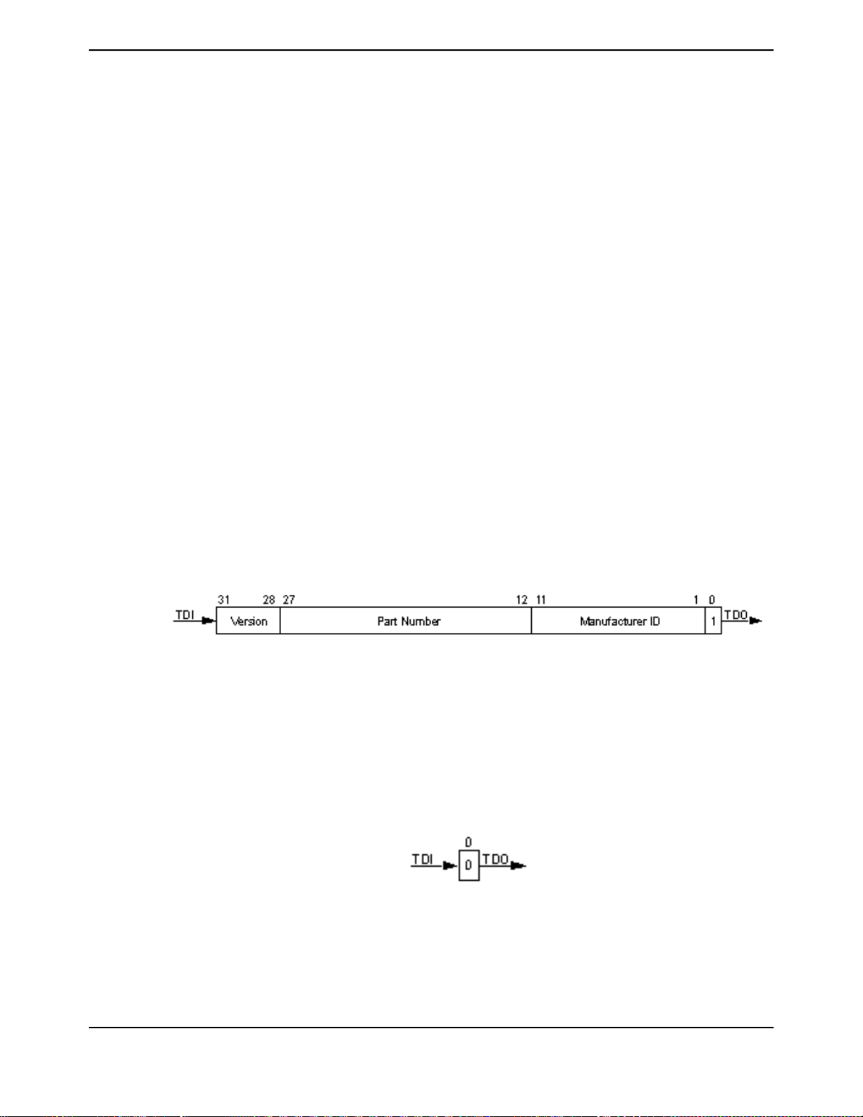
JTAG Interface
5.4.1.8 BYPASS Instruction
The BYPASS instruction connects the associated BYPASS Data Register chain between TDI and
TDO. This instruction is used to create a minimum length serial path between the TDI and TDO ports.
The BYPASS Data Register is a single-bit shift register. This instruction improves test efficiency by
allowing components that are not needed for a specific test to be bypassed in the JTAG scan chain
by loading them with the BYPASS instruction. Please see “BYPASS Data Register” on page 50 for
more information.
5.4.2 Data Registers
The JTAG module contains six Data Registers. These include: IDCODE, BYPASS, Boundary Scan,
APACC, DPACC, and ABORT serial Data Register chains. Each of these Data Registers is discussed
in the following sections.
5.4.2.1 IDCODE Data Register
The format for the 32-bit IDCODE Data Register defined by the IEEE Standard 1149.1 is shown in
Figure 5-3 on page 50. The standard requires that every JTAG-compliant device implement either
the IDCODE instruction or the BYPASS instruction as the default instruction. The LSB of the IDCODE
Data Register is defined to be a 1 to distinguish it from the BYPASS instruction, which has an LSB
of 0. This allows auto configuration test tools to determine which instruction is the default instruction.
The major uses of the JTAG port are for manufacturer testing of component assembly, and program
development and debug. To facilitate the use of auto-configuration debug tools, the IDCODE
instruction outputs a value of 0x1BA00477. This value indicates an ARM Cortex-M3, Version 1
processor. This allows the debuggers to automatically configure themselves to work correctly with
the Cortex-M3 during debug.
Figure 5-3. IDCODE Register Format
5.4.2.2 BYPASS Data Register
The format for the 1-bit BYPASS Data Register defined by the IEEE Standard 1149.1 is shown in
Figure 5-4 on page 50. The standard requires that every JTAG-compliant device implement either
the BYPASS instruction or the IDCODE instruction as the default instruction. The LSB of the BYPASS
Data Register is defined to be a 0 to distinguish it from the IDCODE instruction, which has an LSB
of 1. This allows auto configuration test tools to determine which instruction is the default instruction.
Figure 5-4. BYPASS Register Format
5.4.2.3 Boundary Scan Data Register
The format of the Boundary Scan Data Register is shown in Figure 5-5 on page 51. Each GPIO
pin, in a counter-clockwise direction from the JTAG port pins, is included in the Boundary Scan Data
Register. Each GPIO pin has three associated digital signals that are included in the chain. These
November 29, 200750
Preliminary

O
TDOTDI
O
I
N E
U
T
O
O
I
N E
U
T
O
O
I
N E
U
T
O
O
I
N E
U
T
I
N
...
...
RSTGPIO PB6 GPIOm GPIO m+1 GPIO n
LM3S617 Microcontroller
signals are input, output, and output enable, and are arranged in that order as can be seen in the
figure. In addition to the GPIO pins, the controller reset pin, RST, is included in the chain. Because
the reset pin is always an input, only the input signal is included in the Data Register chain.
When the Boundary Scan Data Register is accessed with the SAMPLE/PRELOAD instruction, the
input, output, and output enable from each digital pad are sampled and then shifted out of the chain
to be verified. The sampling of these values occurs on the rising edge of TCK in the Capture DR
state of the TAP controller. While the sampled data is being shifted out of the Boundary Scan chain
in the Shift DR state of the TAP controller, new data can be preloaded into the chain for use with
the EXTEST and INTEST instructions. These instructions either force data out of the controller, with
the EXTEST instruction, or into the controller, with the INTEST instruction.
Figure 5-5. Boundary Scan Register Format
For detailed information on the order of the input, output, and output enable bits for each of the
GPIO ports, please refer to the Stellaris®Family Boundary Scan Description Language (BSDL) files,
downloadable from www.luminarymicro.com.
5.4.2.4 APACC Data Register
The format for the 35-bit APACC Data Register defined by ARM is described in the ARM®
Cortex™-M3 Technical Reference Manual.
5.4.2.5 DPACC Data Register
The format for the 35-bit DPACC Data Register defined by ARM is described in the ARM®
Cortex™-M3 Technical Reference Manual.
5.4.2.6 ABORT Data Register
The format for the 35-bit ABORT Data Register defined by ARM is described in the ARM®
Cortex™-M3 Technical Reference Manual.
51November 29, 2007
Preliminary

System Control
6 System Control
System control determines the overall operation of the device. It provides information about the
device, controls the clocking to the core and individual peripherals, and handles reset detection and
reporting.
6.1 Functional Description
The System Control module provides the following capabilities:
■ Device identification, see “Device Identification” on page 52
■ Local control, such as reset (see “Reset Control” on page 52), power (see “Power
Control” on page 55) and clock control (see “Clock Control” on page 55)
■ System control (Run, Sleep, and Deep-Sleep modes), see “System Control” on page 58
6.1.1 Device Identification
Seven read-only registers provide software with information on the microcontroller, such as version,
part number, SRAM size, flash size, and other features. See the DID0, DID1, and DC0-DC4 registers.
6.1.2 Reset Control
This section discusses aspects of hardware functions during reset as well as system software
requirements following the reset sequence.
6.1.2.1 Reset Sources
The controller has six sources of reset:
1. External reset input pin (RST) assertion, see “RST Pin Assertion” on page 52.
2. Power-on reset (POR), see “Power-On Reset (POR)” on page 53.
3. Internal brown-out (BOR) detector, see “Brown-Out Reset (BOR)” on page 53.
4. Software-initiated reset (with the software reset registers), see “Software Reset” on page 54.
5. A watchdog timer reset condition violation, see “Watchdog Timer Reset” on page 55.
6. Internal low drop-out (LDO) regulator output
After a reset, the Reset Cause (RESC) register is set with the reset cause. The bits in this register
are sticky and maintain their state across multiple reset sequences,except when an external reset
is the cause, and then all the other bits in the RESC register are cleared.
Note: The main oscillator is used for external resets and power-on resets; the internal oscillator
is used during the internal process by internal reset and clock verification circuitry.
6.1.2.2 RST Pin Assertion
The external reset pin (RST) resets the controller. This resets the core and all the peripherals except
the JTAG TAP controller (see “JTAG Interface” on page 42). The external reset sequence is as
follows:
November 29, 200752
Preliminary

1. The external reset pin (RST) is asserted and then de-asserted.
R
1
C
1
R
2
RST
Stellaris
D
1
2. After RST is de-asserted, the main crystal oscillator is allowed to settle and there is an internal
main oscillator counter that takes from 15-30 ms to account for this. During this time, internal
reset to the rest of the controller is held active.
3. The internal reset is released and the core fetches and loads the initial stack pointer, the initial
program counter, the first instruction designated by the program counter, and begins execution.
The external reset timing is shown in Figure 19-8 on page 395.
6.1.2.3 Power-On Reset (POR)
The Power-On Reset (POR) circuitry detects a rise in power-supply voltage (VDD) and generates
an on-chip reset pulse. To use the on-chip circuitry, the RST input needs to be connected to the
power supply (VDD) through a pull-up resistor (1K to 10K Ω).
The device must be operating within the specified operating parameters at the point when the on-chip
power-on reset pulse is complete. The specified operating parameters include supply voltage,
frequency, temperature, and so on. If the operating conditions are not met at the point of POR end,
the Stellaris®controller does not operate correctly. In this case, the reset must be extended using
external circuitry. The RST input may be used with the circuit as shown in Figure 6-1 on page 53.
LM3S617 Microcontroller
Figure 6-1. External Circuitry to Extend Reset
The R1and C1components define the power-on delay. The R2resistor mitigates any leakage from
the RST input. The diode (D1) discharges C1rapidly when the power supply is turned off.
The Power-On Reset sequence is as follows:
1. The controller waits for the later of external reset (RST) or internal POR to go inactive.
2. After the resets are inactive, the main crystal oscillator is allowed to settle and there is an internal
main oscillator counter that takes from 15-30 ms to account for this. During this time, internal
reset to the rest of the controller is held active.
3. The internal reset is released and the core fetches and loads the initial stack pointer, the initial
program counter, the first instruction designated by the program counter, and begins execution.
The internal POR is only active on the initial power-up of the controller. The Power-On Reset timing
is shown in Figure 19-9 on page 396.
Note: The power-on reset also resets the JTAG controller. An external reset does not.
6.1.2.4 Brown-Out Reset (BOR)
A drop in the input voltage resulting in the assertion of the internal brown-out detector can be used
to reset the controller. This is initially disabled and may be enabled by software.
Preliminary
53November 29, 2007

System Control
The system provides a brown-out detection circuit that triggers if the power supply (VDD) drops
below a brown-out threshold voltage (V
operation of logic and peripherals that operate off the power supply voltage (VDD) and not the LDO
voltage. If a brown-out condition is detected, the system may generate a controller interrupt or a
system reset. The BOR circuit has a digital filter that protects against noise-related detection for the
interrupt condition. This feature may be optionally enabled.
Brown-out resets are controlled with the Power-On and Brown-Out Reset Control (PBORCTL)
register. The BORIOR bit in the PBORCTL register must be set for a brown-out condition to trigger
a reset.
The brown-out reset sequence is as follows:
). The circuit is provided to guard against improper
BTH
1. When VDDdrops below V
2. If the BORWT bit in the PBORCTL register is set and BORIOR is not set, the BOR condition is
resampled again, after a delay specified by BORTIM, to determine if the original condition was
caused by noise. If the BOR condition is not met the second time, then no further action is taken.
3. If the BOR condition exists, an internal reset is asserted.
4. The internal reset is released and the controller fetches and loads the initial stack pointer, the
initial program counter, the first instruction designated by the program counter, and begins
execution.
5. The internal BOR condition is reset after 500 µs to prevent another BOR condition from being
set before software has a chance to investigate the original cause.
The internal Brown-Out Reset timing is shown in Figure 19-10 on page 396.
6.1.2.5 Software Reset
Software can reset a specific peripheral or generate a reset to the entire system .
Peripherals can be individually reset by software via three registers that control reset signals to each
peripheral (see the SRCRn registers). If the bit position corresponding to a peripheral is set and
subsequently cleared, the peripheral is reset. The encoding of the reset registers is consistent with
the encoding of the clock gating control for peripherals and on-chip functions (see “System
Control” on page 58). Note that all reset signals for all clocks of the specified unit are asserted as
a result of a software-initiated reset.
, an internal BOR condition is set.
BTH
The entire system can be reset by software by setting the SYSRESETREQ bit in the Cortex-M3
Application Interrupt and Reset Control register resets the entire system including the core. The
software-initiated system reset sequence is as follows:
1. A software system reset is initiated by writing the SYSRESETREQ bit in the ARM Cortex-M3
Application Interrupt and Reset Control register.
2. An internal reset is asserted.
3. The internal reset is deasserted and the controller loads from memory the initial stack pointer,
the initial program counter, and the first instruction designated by the program counter, and
then begins execution.
The software-initiated system reset timing is shown in Figure 19-11 on page 396.
November 29, 200754
Preliminary

6.1.2.6 Watchdog Timer Reset
The watchdog timer module's function is to prevent system hangs. The watchdog timer can be
configured to generate an interrupt to the controller on its first time-out, and to generate a reset
signal on its second time-out.
After the first time-out event, the 32-bit counter is reloaded with the value of the Watchdog Timer
Load (WDTLOAD) register, and the timer resumes counting down from that value. If the timer counts
down to its zero state again before the first time-out interrupt is cleared, and the reset signal has
been enabled, the watchdog timer asserts its reset signal to the system. The watchdog timer reset
sequence is as follows:
1. The watchdog timer times out for the second time without being serviced.
2. An internal reset is asserted.
3. The internal reset is released and the controller loads from memory the initial stack pointer, the
initial program counter, the first instruction designated by the program counter, and begins
execution.
The watchdog reset timing is shown in Figure 19-12 on page 397.
LM3S617 Microcontroller
6.1.2.7 Low Drop-Out
A reset can be initiated when the internal low drop-out (LDO) regulator output goes unregulated.
This is initially disabled and may be enabled by software. LDO is controlled with the LDO Power
Control (LDOPCTL) register. The LDO reset sequence is as follows:
1. LDO goes unregulated and the LDOARST bit in the LDOARST register is set.
2. An internal reset is asserted.
3. The internal reset is released and the controller fetches and loads the initial stack pointer, the
initial program counter, the first instruction designated by the program counter, and begins
execution.
The LDO reset timing is shown in Figure 19-13 on page 397.
6.1.3 Power Control
The Stellaris®microcontroller provides an integrated LDO regulator that is used to provide power
to the majority of the controller's internal logic. The LDO regulator provides software a mechanism
to adjust the regulated value, in small increments (VSTEP), over the range of 2.25 V to 2.75 V
(inclusive)—or 2.5 V ± 10%. The adjustment is made by changing the value of the VADJ field in the
LDO Power Control (LDOPCTL) register.
6.1.4 Clock Control
System control determines the control of clocks in this part.
6.1.4.1 Fundamental Clock Sources
There are two clock sources for use in the device:
■ Internal Oscillator (IOSC): The internal oscillator is an on-chip clock source. It does not require
the use of any external components. The frequency of the internal oscillator is 12 MHz ± 30%.
55November 29, 2007
Preliminary

Main
Osc
1-8 MHz
Internal
Osc
12 MHz
÷4
OSCSRC
a
OSC1
OSC2
PLL
(200 MHz
output)
BYPASS
a
SYSDIV
a
USESYSDIV
a
System Clock
Constant
Divide
(16.667 MHz output)
ADC Clock
PWMDIV
a
USEPWMDIV
a
PWM Clock
OEN
a
XTAL
a
PWRDN
a
a. These are bit fields within the Run-Mode Clock Configuration (RCC) register.
System Control
■ Main Oscillator: The main oscillator provides a frequency-accurate clock source by one of two
The internal system clock (sysclk), is derived from any of the two sources plus two others: the output
of the internal PLL, and the internal oscillator divided by four (3 MHz ± 30%). The frequency of the
PLL clock reference must be in the range of 3.579545 MHz to 8.192 MHz (inclusive).
Nearly all of the control for the clocks is provided by the Run-Mode Clock Configuration (RCC)
register.
Figure 6-2 on page 56 shows the logic for the main clock tree. The peripheral blocks are driven by
the system clock signal and can be programmatically enabled/disabled. The ADC clock signal is
automatically divided down to 16.67 MHz for proper ADC operation. The PWM clock signal is a
synchronous divide by of the system clock to provide the PWM circuit with more range.
Applications that do not depend on accurate clock sources may use this clock source to reduce
system cost.
means: an external single-ended clock source is connected to the OSC0 input pin, or an external
crystal is connected across the OSC0 input and OSC1 output pins. The crystal value allowed
depends on whether the main oscillator is used as the clock reference source to the PLL. If so,
the crystal must be one of the supported frequencies between 3.579545 MHz through 8.192
MHz (inclusive). If the PLL is not being used, the crystal may be any one of the supported
frequencies between 1 MHz and 8.192 MHz. The single-ended clock source range is from DC
through the specified speed of the device. The supported crystals are listed in the XTAL bit in
the RCC register (see page 70).
Figure 6-2. Main Clock Tree
6.1.4.2 Crystal Configuration for the Main Oscillator (MOSC)
The main oscillator supports the use of a select number of crystals. If the main oscillator is used by
the PLL as a reference clock, the supported range of crystals is 3.579545 to 8.192 MHz, otherwise,
the range of supported crystals is 1 to 8.192 MHz.
The XTAL bit in the RCC register (see page 70) describes the available crystal choices and default
programming values.
Software configures the RCC register XTAL field with the crystal number. If the PLL is used in the
design, the XTAL field value is internally translated to the PLL settings.
Preliminary
November 29, 200756

6.1.4.3 PLL Frequency Configuration
The PLL is disabled by default during power-on reset and is enabled later by software if required.
Software configures the PLL input reference clock source, specifies the output divisor to set the
system clock frequency, and enables the PLL to drive the output.
If the main oscillator provides the clock reference to the PLL, the translation provided by hardware
and used to program the PLL is available for software in the XTAL to PLL Translation (PLLCFG)
register (see page 75). The internal translation provides a translation within ± 1% of the targeted
PLL VCO frequency.
The Crystal Value field (XTAL) on page 70 describes the available crystal choices and default
programming of the PLLCFG register. The crystal number is written into the XTAL field of the
Run-Mode Clock Configuration (RCC) register. Any time the XTAL field changes, the new settings
are translated and the internal PLL settings are updated.
6.1.4.4 PLL Modes
The PLL has two modes of operation: Normal and Power-Down
■ Normal: The PLL multiplies the input clock reference and drives the output.
■ Power-Down: Most of the PLL internal circuitry is disabled and the PLL does not drive the output.
LM3S617 Microcontroller
The modes are programmed using the RCC register fields (see page 70).
6.1.4.5 PLL Operation
If the PLL configuration is changed, the PLL output frequency is unstable until it reconverges (relocks)
to the new setting. The time between the configuration change and relock is T
19-6 on page 390). During this time, the PLL is not usable as a clock reference.
The PLL is changed by one of the following:
■ Change to the XTAL value in the RCC register—writes of the same value do not cause a relock.
■ Change in the PLL from Power-Down to Normal mode.
A counter is defined to measure the T
oscillator. The range of the main oscillator has been taken into account and the down counter is set
to 0x1200 (that is, ~600 μs at an 8.192 MHz external oscillator clock). . Hardware is provided to
keep the PLL from being used as a system clock until the T
two changes above. It is the user's responsibility to have a stable clock source (like the main oscillator)
before the RCC register is switched to use the PLL.
6.1.4.6 Clock Verification Timers
There are three identical clock verification circuits that can be enabled though software. The circuit
checks the faster clock by a slower clock using timers:
■ The main oscillator checks the PLL.
READY
requirement. The counter is clocked by the main
READY
condition is met after one of the
READY
(see Table
■ The main oscillator checks the internal oscillator.
■ The internal oscillator divided by 64 checks the main oscillator.
If the verification timer function is enabled and a failure is detected, the main clock tree is immediately
switched to a working clock and an interrupt is generated to the controller. Software can then
57November 29, 2007
Preliminary

System Control
determine the course of action to take. The actual failure indication and clock switching does not
clear without a write to the CLKVCLR register, an external reset, or a POR reset. The clock
verification timers are controlled by the PLLVER , IOSCVER , and MOSCVER bits in the RCC register.
6.1.5 System Control
For power-savings purposes, the RCGCn , SCGCn , and DCGCn registers control the clock gating
logic for each peripheral or block in the system while the controller is in Run, Sleep, and Deep-Sleep
mode, respectively. The DC1 , DC2 and DC4 registers act as a write mask for the RCGCn , SCGCn,
and DCGCn registers.
In Run mode, the controller is actively executing code. In Sleep mode, the clocking of the device is
unchanged but the controller no longer executes code (and is no longer clocked). In Deep-Sleep
mode, the clocking of the device may change (depending on the Run mode clock configuration)
and the controller no longer executes code (and is no longer clocked). An interrupt returns the device
to Run mode from one of the sleep modes. Each mode is described in more detail in this section.
There are four levels of operation for the device defined as:
■ Run Mode. Run mode provides normal operation of the processor and all of the peripherals that
are currently enabled by the RCGCn registers. The system clock can be any of the available
clock sources including the PLL.
■ Sleep Mode. Sleep mode is entered by the Cortex-M3 core executing a WFI (Wait for
Interrupt) instruction. Any properly configured interrupt event in the system will bring the
processor back into Run mode. See the system control NVIC section of the ARM® Cortex™-M3
Technical Reference Manual for more details.
In Sleep mode, the Cortex-M3 processor core and the memory subsystem are not clocked.
Peripherals are clocked that are enabled in the SCGCn register when auto-clock gating is enabled
(see the RCC register) or the RCGCn register when the auto-clock gating is disabled. The system
clock has the same source and frequency as that during Run mode.
■ Deep-Sleep Mode. Deep-Sleep mode is entered by first writing the Deep Sleep Enable bit in
the ARM Cortex-M3 NVIC system control register and then executing a WFI instruction. Any
properly configured interrupt event in the system will bring the processor back into Run mode.
See the system control NVIC section of the ARM® Cortex™-M3 Technical Reference Manual
for more details.
The Cortex-M3 processor core and the memory subsystem are not clocked. Peripherals are
clocked that are enabled in the DCGCn register when auto-clock gating is enabled (see the RCC
register) or the RCGCn register when auto-clock gating is disabled. The system clock source is
the main oscillator by default or the internal oscillator specified in the DSLPCLKCFG register if
one is enabled. When the DSLPCLKCFG register is used, the internal oscillator is powered up,
if necessary, and the main oscillator is powered down. If the PLL is running at the time of the
WFI instruction, hardware will power the PLL down and override the SYSDIV field of the active
RCC register to be /16 or /64, respectively. When the Deep-Sleep exit event occurs, hardware
brings the system clock back to the source and frequency it had at the onset of Deep-Sleep
mode before enabling the clocks that had been stopped during the Deep-Sleep duration.
6.2 Initialization and Configuration
The PLL is configured using direct register writes to the RCC register. The steps required to
successfully change the PLL-based system clock are:
Preliminary
November 29, 200758

1. Bypass the PLL and system clock divider by setting the BYPASS bit and clearing the USESYS
bit in the RCC register. This configures the system to run off a “raw” clock source (using the
main oscillator or internal oscillator) and allows for the new PLL configuration to be validated
before switching the system clock to the PLL.
2. Select the crystal value (XTAL) and oscillator source (OSCSRC), and clear the PWRDN and OEN
bits in RCC. Setting the XTAL field automatically pulls valid PLL configuration data for the
appropriate crystal, and clearing the PWRDN and OEN bits powers and enables the PLL and its
output.
3. Select the desired system divider (SYSDIV) in RCC and set the USESYS bit in RCC. The SYSDIV
field determines the system frequency for the microcontroller.
4. Wait for the PLL to lock by polling the PLLLRIS bit in the Raw Interrupt Status (RIS) register.
5. Enable use of the PLL by clearing the BYPASS bit in RCC.
Note: If the BYPASS bit is cleared before the PLL locks, it is possible to render the device unusable.
6.3 Register Map
LM3S617 Microcontroller
Table 6-1 on page 59 lists the System Control registers, grouped by function. The offset listed is a
hexadecimal increment to the register’s address, relative to the System Control base address of
0x400F.E000.
Note: Spaces in the System Control register space that are not used are reserved for future or
internal use by Luminary Micro, Inc. Software should not modify any reserved memory
address.
Table 6-1. System Control Register Map
DescriptionResetTypeNameOffset
See
page
61Device Identification 0-RODID00x000
79Device Identification 1-RODID10x004
81Device Capabilities 00x001F.000FRODC00x008
82Device Capabilities 10x0011.32BFRODC10x010
84Device Capabilities 20x0107.0013RODC20x014
86Device Capabilities 30x3F3F.01FFRODC30x018
88Device Capabilities 40x0000.001FRODC40x01C
63Power-On and Brown-Out Reset Control0x0000.7FFDR/WPBORCTL0x030
64LDO Power Control0x0000.0000R/WLDOPCTL0x034
Preliminary
107Software Reset Control 00x00000000R/WSRCR00x040
108Software Reset Control 10x00000000R/WSRCR10x044
109Software Reset Control 20x00000000R/WSRCR20x048
65Raw Interrupt Status0x0000.0000RORIS0x050
66Interrupt Mask Control0x0000.0000R/WIMC0x054
59November 29, 2007

System Control
DescriptionResetTypeNameOffset
See
page
68Masked Interrupt Status and Clear0x0000.0000R/W1CMISC0x058
69Reset Cause-R/WRESC0x05C
70Run-Mode Clock Configuration0x07AE.3AD1R/WRCC0x060
75XTAL to PLL Translation-ROPLLCFG0x064
89Run Mode Clock Gating Control Register 00x00000040R/WRCGC00x100
95Run Mode Clock Gating Control Register 10x00000000R/WRCGC10x104
101Run Mode Clock Gating Control Register 20x00000000R/WRCGC20x108
91Sleep Mode Clock Gating Control Register 00x00000040R/WSCGC00x110
97Sleep Mode Clock Gating Control Register 10x00000000R/WSCGC10x114
103Sleep Mode Clock Gating Control Register 20x00000000R/WSCGC20x118
93Deep Sleep Mode Clock Gating Control Register 00x00000040R/WDCGC00x120
99Deep Sleep Mode Clock Gating Control Register 10x00000000R/WDCGC10x124
105Deep Sleep Mode Clock Gating Control Register 20x00000000R/WDCGC20x128
76Deep Sleep Clock Configuration0x0780.0000R/WDSLPCLKCFG0x144
77Clock Verification Clear0x0000.0000R/WCLKVCLR0x150
6.4 Register Descriptions
All addresses given are relative to the System Control base address of 0x400F.E000.
78Allow Unregulated LDO to Reset the Part0x0000.0000R/WLDOARST0x160
Preliminary
November 29, 200760

Register 1: Device Identification 0 (DID0), offset 0x000
This register identifies the version of the device.
Device Identification 0 (DID0)
Base 0x400F.E000
Offset 0x000
Type RO, reset -
LM3S617 Microcontroller
16171819202122232425262728293031
reservedVERreserved
ROROROROROROROROROROROROROROROROType
0000000000000000Reset
0123456789101112131415
MINORMAJOR
ROROROROROROROROROROROROROROROROType
----------------Reset
DescriptionResetTypeNameBit/Field
0ROreserved31
Software should not rely on the value of a reserved bit. To provide
compatibility with future products, the value of a reserved bit should be
preserved across a read-modify-write operation.
0x0ROVER30:28
DID0 Version
This field defines the DID0 register format version. The version number
is numeric. The value of the VER field is encoded as follows:
DescriptionValue
Initial DID0 register format definition for Stellaris®
0x0
Sandstorm-class devices.
0x0ROreserved27:16
Software should not rely on the value of a reserved bit. To provide
compatibility with future products, the value of a reserved bit should be
preserved across a read-modify-write operation.
-ROMAJOR15:8
Major Revision
This field specifies the major revision number of the device. The major
revision reflects changes to base layers of the design. The major revision
number is indicated in the part number as a letter (A for first revision, B
for second, and so on). This field is encoded as follows:
DescriptionValue
Revision A (initial device)0x0
Revision B (first base layer revision)0x1
Revision C (second base layer revision)0x2
and so on.
Preliminary
61November 29, 2007

System Control
DescriptionResetTypeNameBit/Field
-ROMINOR7:0
Minor Revision
This field specifies the minor revision number of the device. The minor
revision reflects changes to the metal layers of the design. The MINOR
field value is reset when the MAJOR field is changed. This field is numeric
and is encoded as follows:
DescriptionValue
Initial device, or a major revision update.0x0
First metal layer change.0x1
Second metal layer change.0x2
and so on.
Preliminary
November 29, 200762
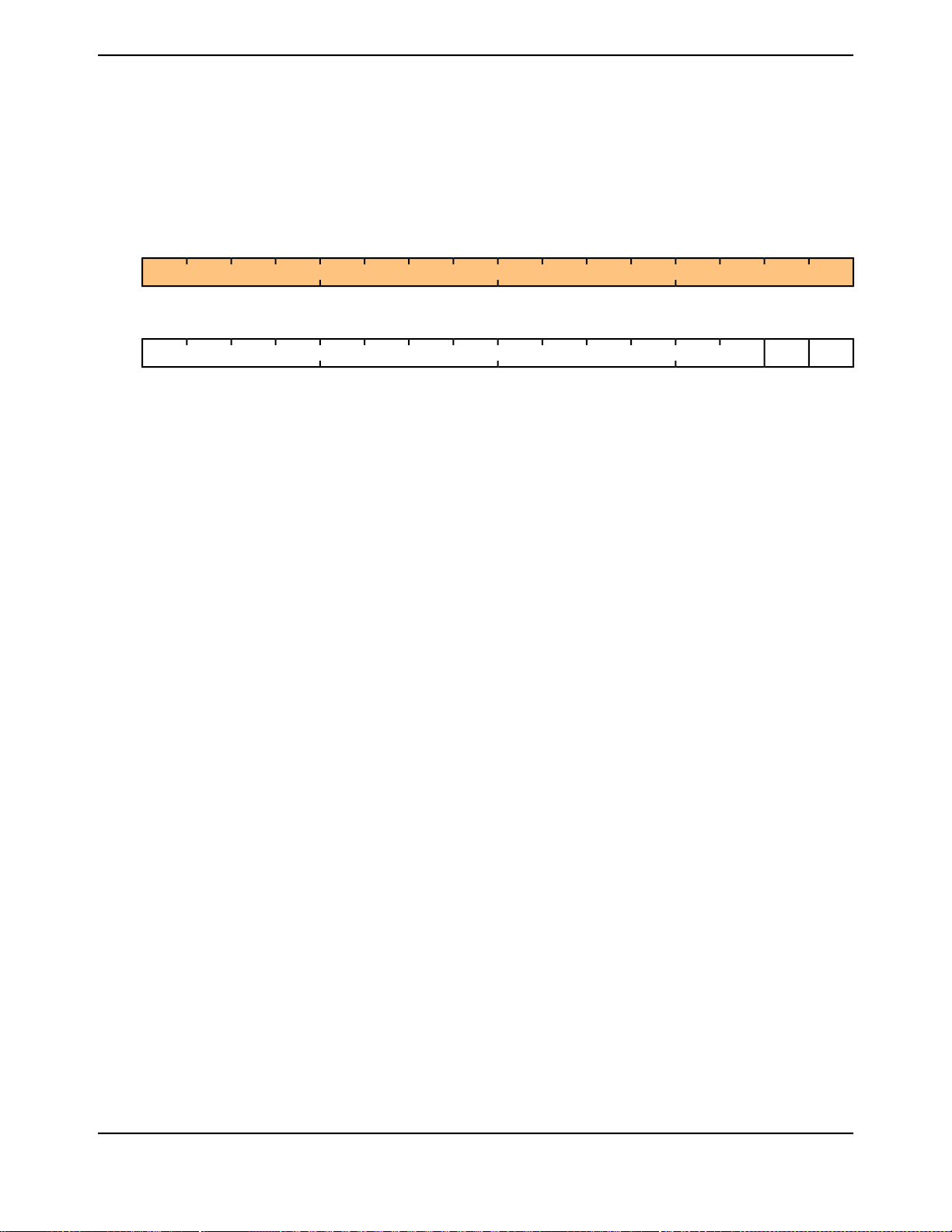
Register 2: Power-On and Brown-Out Reset Control (PBORCTL), offset 0x030
This register is responsible for controlling reset conditions after initial power-on reset.
Power-On and Brown-Out Reset Control (PBORCTL)
Base 0x400F.E000
Offset 0x030
Type R/W, reset 0x0000.7FFD
DescriptionResetTypeNameBit/Field
reserved
LM3S617 Microcontroller
16171819202122232425262728293031
ROROROROROROROROROROROROROROROROType
0000000000000000Reset
0123456789101112131415
BORWTBORIORBORTIM
R/WR/WR/WR/WR/WR/WR/WR/WR/WR/WR/WR/WR/WR/WR/WR/WType
1011111111111110Reset
0x0ROreserved31:16
Software should not rely on the value of a reserved bit. To provide
compatibility with future products, the value of a reserved bit should be
preserved across a read-modify-write operation.
0x1FFFR/WBORTIM15:2
BOR Time Delay
This field specifies the number of internal oscillator clocks delayed before
the BOR output is resampled if the BORWT bit is set.
The width of this field is derived by the t
width of 500 μs and the
BOR
internal oscillator (IOSC) frequency of 12 MHz ± 30%. At +30%, the
counter value has to exceed 7,800.
0R/WBORIOR1
BOR Interrupt or Reset
This bit controls how a BOR event is signaled to the controller. If set, a
reset is signaled. Otherwise, an interrupt is signaled.
1R/WBORWT0
BOR Wait and Check for Noise
This bit specifies the response to a brown-out signal assertion if BORIOR
is not set.
If BORWT is set to 1 and BORIOR is cleared to 0, the controller waits
BORTIM IOSC periods and resamples the BOR output. If still asserted,
a BOR interrupt is signalled. If no longer asserted, the initial assertion
is suppressed (attributable to noise).
If BORWT is 0, BOR assertions do not resample the output and any
condition is reported immediately if enabled.
Preliminary
63November 29, 2007
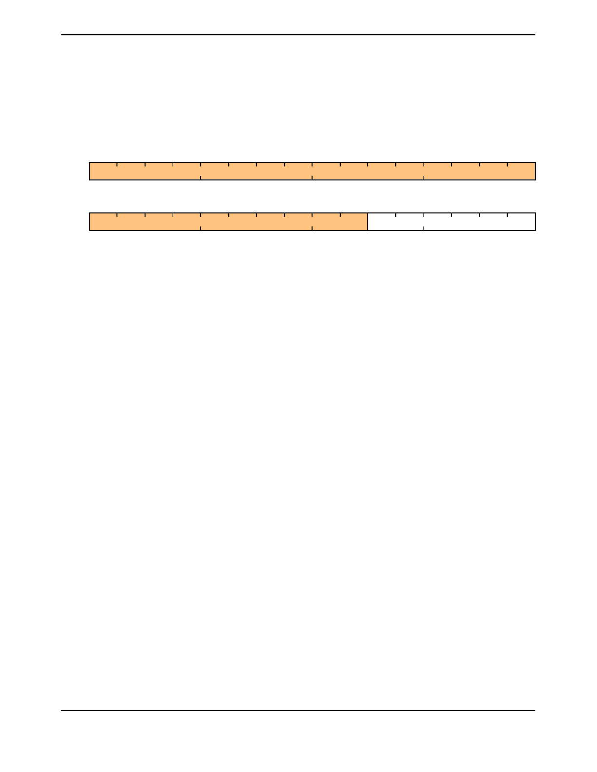
System Control
Register 3: LDO Power Control (LDOPCTL), offset 0x034
The VADJ field in this register adjusts the on-chip output voltage (V
LDO Power Control (LDOPCTL)
Base 0x400F.E000
Offset 0x034
Type R/W, reset 0x0000.0000
).
OUT
16171819202122232425262728293031
reserved
ROROROROROROROROROROROROROROROROType
0000000000000000Reset
0123456789101112131415
VADJreserved
R/WR/WR/WR/WR/WR/WROROROROROROROROROROType
0000000000000000Reset
DescriptionResetTypeNameBit/Field
0ROreserved31:6
Software should not rely on the value of a reserved bit. To provide
compatibility with future products, the value of a reserved bit should be
preserved across a read-modify-write operation.
0x0R/WVADJ5:0
LDO Output Voltage
This field sets the on-chip output voltage. The programming values for
the VADJ field are provided below.
V
(V)Value
OUT
2.500x00
2.450x01
2.400x02
2.350x03
2.300x04
2.250x05
Reserved0x06-0x3F
2.750x1B
2.700x1C
2.650x1D
2.600x1E
2.550x1F
Preliminary
November 29, 200764

Register 4: Raw Interrupt Status (RIS), offset 0x050
Central location for system control raw interrupts. These are set and cleared by hardware.
Raw Interrupt Status (RIS)
Base 0x400F.E000
Offset 0x050
Type RO, reset 0x0000.0000
DescriptionResetTypeNameBit/Field
reserved
LM3S617 Microcontroller
16171819202122232425262728293031
ROROROROROROROROROROROROROROROROType
0000000000000000Reset
0123456789101112131415
PLLFRISBORRISLDORISMOFRISIOFRISCLRISPLLLRISreserved
ROROROROROROROROROROROROROROROROType
0000000000000000Reset
0ROreserved31:7
Software should not rely on the value of a reserved bit. To provide
compatibility with future products, the value of a reserved bit should be
preserved across a read-modify-write operation.
0ROPLLLRIS6
0ROCLRIS5
PLL Lock Raw Interrupt Status
This bit is set when the PLL T
READY
Current Limit Raw Interrupt Status
Timer asserts.
This bit is set if the LDO’s CLE output asserts.
0ROIOFRIS4
Internal Oscillator Fault Raw Interrupt Status
This bit is set if an internal oscillator fault is detected.
0ROMOFRIS3
Main Oscillator Fault Raw Interrupt Status
This bit is set if a main oscillator fault is detected.
0ROLDORIS2
LDO Power Unregulated Raw Interrupt Status
This bit is set if a LDO voltage is unregulated.
0ROBORRIS1
Brown-Out Reset Raw Interrupt Status
This bit is the raw interrupt status for any brown-out conditions. If set,
a brown-out condition is currently active. This is an unregistered signal
from the brown-out detection circuit. An interrupt is reported if the BORIM
bit in the IMC register is set and the BORIOR bit in the PBORCTL register
is cleared.
0ROPLLFRIS0
Preliminary
PLL Fault Raw Interrupt Status
This bit is set if a PLL fault is detected (stops oscillating).
65November 29, 2007
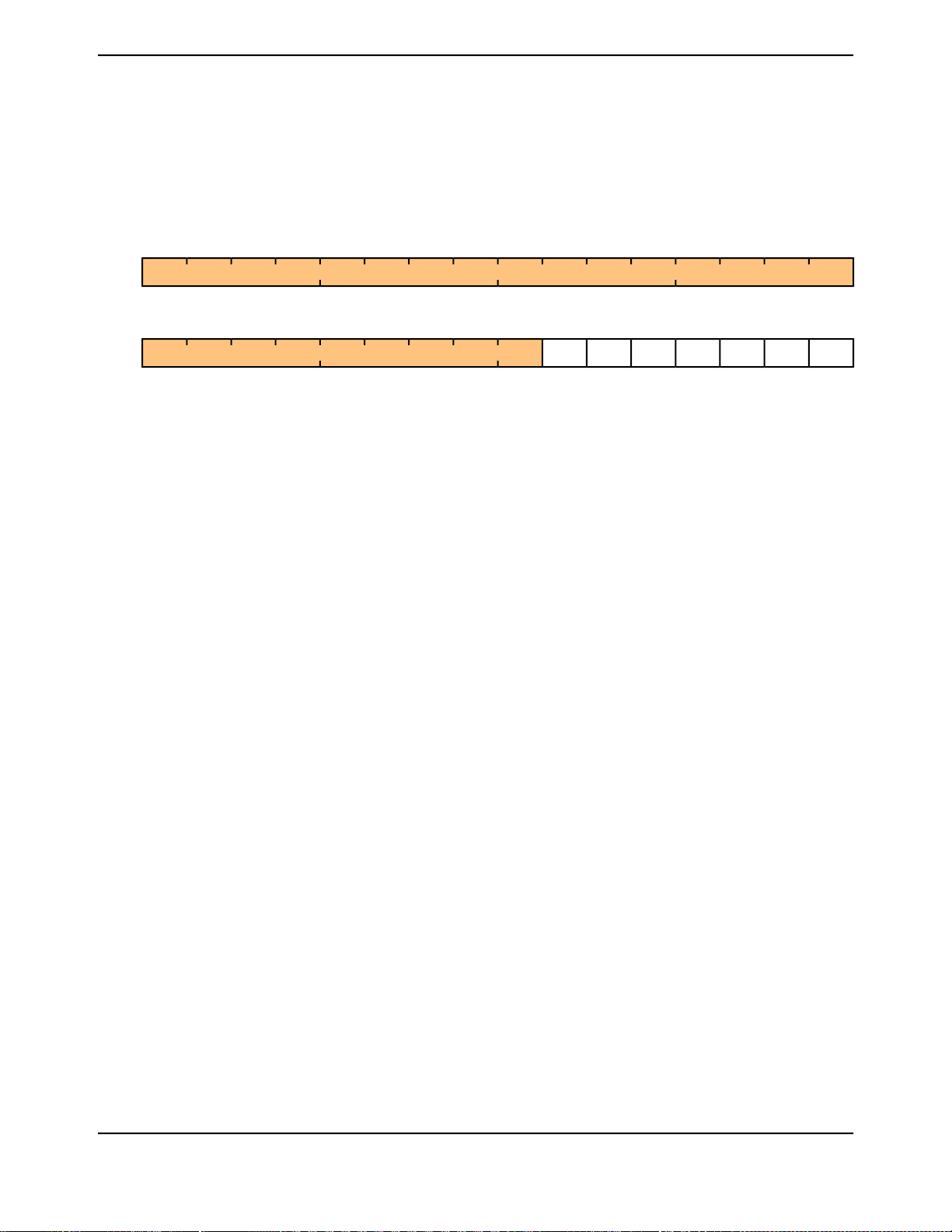
System Control
Register 5: Interrupt Mask Control (IMC), offset 0x054
Central location for system control interrupt masks.
Interrupt Mask Control (IMC)
Base 0x400F.E000
Offset 0x054
Type R/W, reset 0x0000.0000
DescriptionResetTypeNameBit/Field
reserved
16171819202122232425262728293031
ROROROROROROROROROROROROROROROROType
0000000000000000Reset
0123456789101112131415
PLLFIMBORIMLDOIMMOFIMIOFIMCLIMPLLLIMreserved
R/WR/WR/WR/WR/WR/WR/WROROROROROROROROROType
0000000000000000Reset
0ROreserved31:7
Software should not rely on the value of a reserved bit. To provide
compatibility with future products, the value of a reserved bit should be
preserved across a read-modify-write operation.
0R/WPLLLIM6
PLL Lock Interrupt Mask
This bit specifies whether a current limit detection is promoted to a
controller interrupt. If set, an interrupt is generated if PLLLRIS in RIS
is set; otherwise, an interrupt is not generated.
0R/WCLIM5
Current Limit Interrupt Mask
This bit specifies whether a current limit detection is promoted to a
controller interrupt. If set, an interrupt is generated if CLRIS is set;
otherwise, an interrupt is not generated.
0R/WIOFIM4
Internal Oscillator Fault Interrupt Mask
This bit specifies whether an internal oscillator fault detection is promoted
to a controller interrupt. If set, an interrupt is generated if IOFRIS is set;
otherwise, an interrupt is not generated.
0R/WMOFIM3
Main Oscillator Fault Interrupt Mask
This bit specifies whether a main oscillator fault detection is promoted
to a controller interrupt. If set, an interrupt is generated if MOFRIS is set;
otherwise, an interrupt is not generated.
0R/WLDOIM2
LDO Power Unregulated Interrupt Mask
This bit specifies whether an LDO unregulated power situation is
promoted to a controller interrupt. If set, an interrupt is generated if
LDORIS is set; otherwise, an interrupt is not generated.
0R/WBORIM1
Preliminary
Brown-Out Reset Interrupt Mask
This bit specifies whether a brown-out condition is promoted to a
controller interrupt. If set, an interrupt is generated if BORRIS is set;
otherwise, an interrupt is not generated.
November 29, 200766

LM3S617 Microcontroller
DescriptionResetTypeNameBit/Field
0R/WPLLFIM0
PLL Fault Interrupt Mask
This bit specifies whether a PLL fault detection is promoted to a controller
interrupt. If set, an interrupt is generated if PLLFRIS is set; otherwise,
an interrupt is not generated.
Preliminary
67November 29, 2007

System Control
Register 6: Masked Interrupt Status and Clear (MISC), offset 0x058
Central location for system control result of RIS AND IMC to generate an interrupt to the controller.
All of the bits are R/W1C and this action also clears the corresponding raw interrupt bit in the RIS
register (see page 65).
Masked Interrupt Status and Clear (MISC)
Base 0x400F.E000
Offset 0x058
Type R/W1C, reset 0x0000.0000
DescriptionResetTypeNameBit/Field
reserved
16171819202122232425262728293031
ROROROROROROROROROROROROROROROROType
0000000000000000Reset
0123456789101112131415
reservedBORMISLDOMISMOFMISIOFMISCLMISPLLLMISreserved
ROR/W1CR/W1CR/W1CR/W1CR/W1CR/W1CROROROROROROROROROType
0000000000000000Reset
0ROreserved31:7
Software should not rely on the value of a reserved bit. To provide
compatibility with future products, the value of a reserved bit should be
preserved across a read-modify-write operation.
0R/W1CPLLLMIS6
PLL Lock Masked Interrupt Status
This bit is set when the PLL T
READY
timer asserts. The interrupt is cleared
by writing a 1 to this bit.
0R/W1CCLMIS5
Current Limit Masked Interrupt Status
This bit is set if the LDO’s CLE output asserts. The interrupt is cleared
by writing a 1 to this bit.
0R/W1CIOFMIS4
Internal Oscillator Fault Masked Interrupt Status
This bit is set if an internal oscillator fault is detected. The interrupt is
cleared by writing a 1 to this bit.
0R/W1CMOFMIS3
Main Oscillator Fault Masked Interrupt Status
This bit is set if a main oscillator fault is detected. The interrupt is cleared
by writing a 1 to this bit.
0R/W1CLDOMIS2
LDO Power Unregulated Masked Interrupt Status
This bit is set if LDO power is unregulated. The interrupt is cleared by
writing a 1 to this bit.
0R/W1CBORMIS1
BOR Masked Interrupt Status
This bit is the masked interrupt status for any brown-out conditions. If
set, a brown-out condition was detected. An interrupt is reported if the
BORIM bit in the IMC register is set and the BORIOR bit in the PBORCTL
register is cleared. The interrupt is cleared by writing a 1 to this bit.
0ROreserved0
Preliminary
Software should not rely on the value of a reserved bit. To provide
compatibility with future products, the value of a reserved bit should be
preserved across a read-modify-write operation.
November 29, 200768

Register 7: Reset Cause (RESC), offset 0x05C
This field specifies the cause of the reset event to software. The reset value is determined by the
cause of the reset. When an external reset is the cause (EXT is set), all other reset bits are cleared.
However, if the reset is due to any other cause, the remaining bits are sticky, allowing software to
see all causes.
Reset Cause (RESC)
Base 0x400F.E000
Offset 0x05C
Type R/W, reset -
DescriptionResetTypeNameBit/Field
reserved
LM3S617 Microcontroller
16171819202122232425262728293031
ROROROROROROROROROROROROROROROROType
0000000000000000Reset
0123456789101112131415
EXTPORBORWDTSWLDOreserved
R/WR/WR/WR/WR/WR/WROROROROROROROROROROType
------0000000000Reset
0ROreserved31:6
Software should not rely on the value of a reserved bit. To provide
compatibility with future products, the value of a reserved bit should be
preserved across a read-modify-write operation.
-R/WLDO5
LDO Reset
When set, indicates the LDO circuit has lost regulation and has
generated a reset event.
-R/WSW4
Software Reset
When set, indicates a software reset is the cause of the reset event.
-R/WWDT3
Watchdog Timer Reset
When set, indicates a watchdog reset is the cause of the reset event.
-R/WBOR2
Brown-Out Reset
When set, indicates a brown-out reset is the cause of the reset event.
-R/WPOR1
Power-On Reset
When set, indicates a power-on reset is the cause of the reset event.
-R/WEXT0
External Reset
When set, indicates an external reset (RST assertion) is the cause of
the reset event.
Preliminary
69November 29, 2007
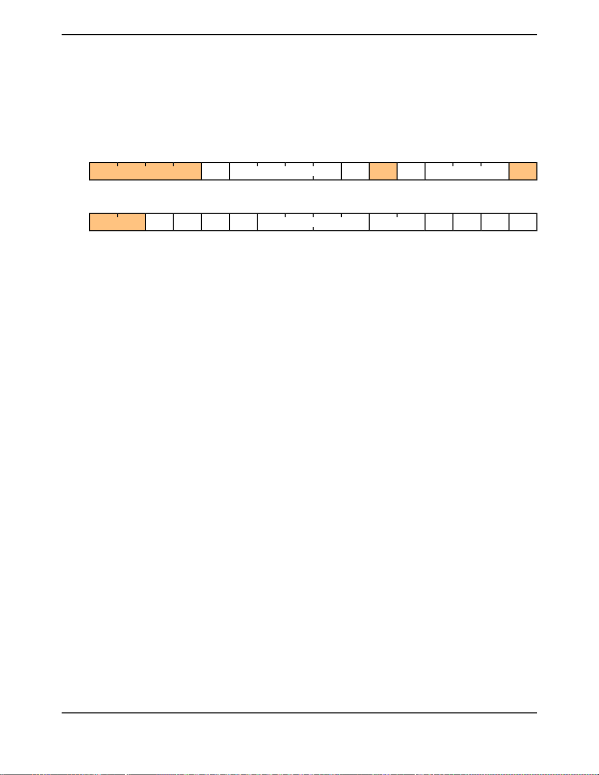
System Control
Register 8: Run-Mode Clock Configuration (RCC), offset 0x060
This register is defined to provide source control and frequency speed.
Run-Mode Clock Configuration (RCC)
Base 0x400F.E000
Offset 0x060
Type R/W, reset 0x07AE.3AD1
16171819202122232425262728293031
SYSDIVACGreserved
USESYSDIV
reserved
USEPWMDIV
reservedPWMDIV
ROR/WR/WR/WR/WROR/WR/WR/WR/WR/WR/WROROROROType
0111000111100000Reset
0123456789101112131415
MOSCDISIOSCDISMOSCVERIOSCVEROSCSRCXTALPLLVERBYPASSOENPWRDNreserved
R/WR/WR/WR/WR/WR/WR/WR/WR/WR/WR/WR/WR/WR/WROROType
1000001101011100Reset
DescriptionResetTypeNameBit/Field
0x0ROreserved31:28
Software should not rely on the value of a reserved bit. To provide
compatibility with future products, the value of a reserved bit should be
preserved across a read-modify-write operation.
0R/WACG27
Auto Clock Gating
This bit specifies whether the system uses the Sleep-Mode Clock
Gating Control (SCGCn) registers and Deep-Sleep-Mode Clock
Gating Control (DCGCn) registers if the controller enters a Sleep or
Deep-Sleep mode (respectively). If set, the SCGCn or DCGCn registers
are used to control the clocks distributed to the peripherals when the
controller is in a sleep mode. Otherwise, the Run-Mode Clock Gating
Control (RCGCn) registers are used when the controller enters a sleep
mode.
The RCGCn registers are always used to control the clocks in Run
mode.
This allows peripherals to consume less power when the controller is
in a sleep mode and the peripheral is unused.
Preliminary
November 29, 200770

LM3S617 Microcontroller
DescriptionResetTypeNameBit/Field
0xFR/WSYSDIV26:23
System Clock Divisor
Specifies which divisor is used to generate the system clock from the
PLL output.
The PLL VCO frequency is 200 MHz.
Frequency (BYPASS=0)Divisor (BYPASS=1)Value
reservedreserved0x0
reserved/20x1
reserved/30x2
50 MHz/40x3
40 MHz/50x4
33.33 MHz/60x5
28.57 MHz/70x6
25 MHz/80x7
22.22 MHz/90x8
20 MHz/100x9
18.18 MHz/110xA
16.67 MHz/120xB
15.38 MHz/130xC
14.29 MHz/140xD
13.33 MHz/150xE
12.5 MHz (default)/160xF
When reading the Run-Mode Clock Configuration (RCC) register (see
page 70), the SYSDIV value is MINSYSDIV if a lower divider was
requested and the PLL is being used. This lower value is allowed to
divide a non-PLL source.
0R/WUSESYSDIV22
0ROreserved21
0R/WUSEPWMDIV20
Enable System Clock Divider
Use the system clock divider as the source for the system clock. The
system clock divider is forced to be used when the PLL is selected as
the source.
Software should not rely on the value of a reserved bit. To provide
compatibility with future products, the value of a reserved bit should be
preserved across a read-modify-write operation.
Enable PWM Clock Divisor
Use the PWM clock divider as the source for the PWM clock.
Preliminary
71November 29, 2007

System Control
DescriptionResetTypeNameBit/Field
0x7R/WPWMDIV19:17
0ROreserved16:14
1R/WPWRDN13
PWM Unit Clock Divisor
This field specifies the binary divisor used to predivide the system clock
down for use as the timing reference for the PWM module. This clock
is only power 2 divide and rising edge is synchronous without phase
shift from the system clock.
DivisorValue
/20x0
/40x1
/80x2
/160x3
/320x4
/640x5
/640x6
/64 (default)0x7
Software should not rely on the value of a reserved bit. To provide
compatibility with future products, the value of a reserved bit should be
preserved across a read-modify-write operation.
PLL Power Down
This bit connects to the PLL PWRDN input. The reset value of 1 powers
down the PLL. See Table 6-2 on page 74 for PLL mode control.
1R/WOEN12
1R/WBYPASS11
0R/WPLLVER10
PLL Output Enable
This bit specifies whether the PLL output driver is enabled. If cleared,
the driver transmits the PLL clock to the output. Otherwise, the PLL
clock does not oscillate outside the PLL module.
Note: Both PWRDN and OEN must be cleared to run the PLL.
PLL Bypass
Chooses whether the system clock is derived from the PLL output or
the OSC source. If set, the clock that drives the system is the OSC
source. Otherwise, the clock that drives the system is the PLL output
clock divided by the system divider.
Note: The ADC must be clocked from the PLL or directly from a
14-MHz to 18-MHz clock source to operate properly.
PLL Verification
This bit controls the PLL verification timer function. If set, the verification
timer is enabled and an interrupt is generated if the PLL becomes
inoperative. Otherwise, the verification timer is not enabled.
Preliminary
November 29, 200772

LM3S617 Microcontroller
DescriptionResetTypeNameBit/Field
0xBR/WXTAL9:6
Crystal Value
This field specifies the crystal value attached to the main oscillator. The
encoding for this field is provided below.
Value
Crystal Frequency (MHz)
Not Using the PLL
6 MHz (reset value)0xB
Crystal Frequency (MHz)
Using the PLL
reserved1.0000x0
reserved1.84320x1
reserved2.0000x2
reserved2.45760x3
3.579545 MHz0x4
3.6864 MHz0x5
4 MHz0x6
4.096 MHz0x7
4.9152 MHz0x8
5 MHz0x9
5.12 MHz0xA
6.144 MHz0xC
7.3728 MHz0xD
8 MHz0xE
8.192 MHz0xF
0x0R/WOSCSRC5:4
0R/WIOSCVER3
0R/WMOSCVER2
0R/WIOSCDIS1
Oscillator Source
Picks among the four input sources for the OSC. The values are:
Input SourceValue
Main oscillator (default)0x0
Internal oscillator (default)0x1
Internal oscillator / 4 (this is necessary if used as input to PLL)0x2
reserved0x3
Internal Oscillator Verification Timer
This bit controls the internal oscillator verification timer function. If set,
the verification timer is enabled and an interrupt is generated if the timer
becomes inoperative. Otherwise, the verification timer is not enabled.
Main Oscillator Verification Timer
This bit controls the main oscillator verification timer function. If set, the
verification timer is enabled and an interrupt is generated if the timer
becomes inoperative. Otherwise, the verification timer is not enabled.
Internal Oscillator Disable
0: Internal oscillator (IOSC) is enabled.
1: Internal oscillator is disabled.
Preliminary
73November 29, 2007

System Control
DescriptionResetTypeNameBit/Field
Table 6-2. PLL Mode Control
ModeOENPWRDN
Power downX1
Normal00
1R/WMOSCDIS0
Main Oscillator Disable
0: Main oscillator is enabled.
1: Main oscillator is disabled (default).
Preliminary
November 29, 200774
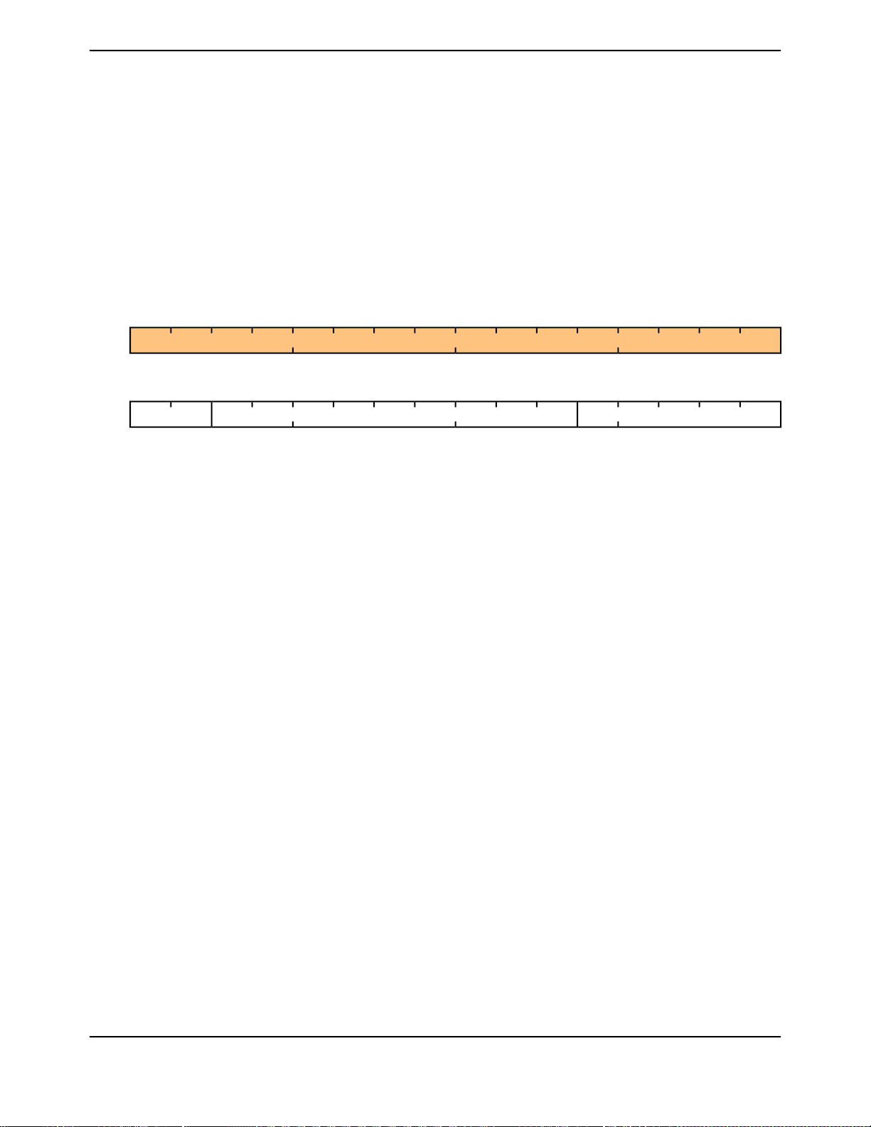
Register 9: XTAL to PLL Translation (PLLCFG), offset 0x064
This register provides a means of translating external crystal frequencies into the appropriate PLL
settings. This register is initialized during the reset sequence and updated anytime that the XTAL
field changes in the Run-Mode Clock Configuration (RCC) register (see page 70).
The PLL frequency is calculated using the PLLCFG field values, as follows:
PLLFreq = OSCFreq * (F + 2) / (R + 2)
XTAL to PLL Translation (PLLCFG)
Base 0x400F.E000
Offset 0x064
Type RO, reset -
reserved
LM3S617 Microcontroller
16171819202122232425262728293031
ROROROROROROROROROROROROROROROROType
0000000000000000Reset
0123456789101112131415
RFOD
ROROROROROROROROROROROROROROROROType
----------------Reset
DescriptionResetTypeNameBit/Field
0x0ROreserved31:16
Software should not rely on the value of a reserved bit. To provide
compatibility with future products, the value of a reserved bit should be
preserved across a read-modify-write operation.
-ROOD15:14
PLL OD Value
This field specifies the value supplied to the PLL’s OD input.
DescriptionValue
Divide by 10x0
Divide by 20x1
Divide by 40x2
Reserved0x3
-ROF13:5
PLL F Value
This field specifies the value supplied to the PLL’s F input.
-ROR4:0
PLL R Value
This field specifies the value supplied to the PLL’s R input.
Preliminary
75November 29, 2007

System Control
Register 10: Deep Sleep Clock Configuration (DSLPCLKCFG), offset 0x144
This register is used to automatically switch from the main oscillator to the internal oscillator when
entering Deep-Sleep mode. The system clock source is the main oscillator by default. When this
register is set, the internal oscillator is powered up and the main oscillator is powered down. When
the Deep-Sleep exit event occurs, hardware brings the system clock back to the source and frequency
it had at the onset of Deep-Sleep mode.
Deep Sleep Clock Configuration (DSLPCLKCFG)
Base 0x400F.E000
Offset 0x144
Type R/W, reset 0x0780.0000
reserved
16171819202122232425262728293031
ROROROROROROROROROROROROROROROROType
0000000000000000Reset
0123456789101112131415
IOSCreserved
R/WROROROROROROROROROROROROROROROType
0000000000000000Reset
DescriptionResetTypeNameBit/Field
0x0ROreserved31:1
Software should not rely on the value of a reserved bit. To provide
compatibility with future products, the value of a reserved bit should be
preserved across a read-modify-write operation.
0R/WIOSC0
IOSC Clock Source
When set, forces IOSC to be clock source during Deep-Sleep (overrides
DSOSCSRC field if set)
Preliminary
November 29, 200776

Register 11: Clock Verification Clear (CLKVCLR), offset 0x150
This register is provided as a means of clearing the clock verification circuits by software. Since the
clock verification circuits force a known good clock to control the process, the controller is allowed
the opportunity to solve the problem and clear the verification fault. This register clears all clock
verification faults. To clear a clock verification fault, the VERCLR bit must be set and then cleared
by software. This bit is not self-clearing.
Clock Verification Clear (CLKVCLR)
Base 0x400F.E000
Offset 0x150
Type R/W, reset 0x0000.0000
reserved
LM3S617 Microcontroller
16171819202122232425262728293031
ROROROROROROROROROROROROROROROROType
0000000000000000Reset
0123456789101112131415
VERCLRreserved
R/WROROROROROROROROROROROROROROROType
0000000000000000Reset
DescriptionResetTypeNameBit/Field
0ROreserved31:1
Software should not rely on the value of a reserved bit. To provide
compatibility with future products, the value of a reserved bit should be
preserved across a read-modify-write operation.
0R/WVERCLR0
Clock Verification Clear
Clears clock verification faults.
Preliminary
77November 29, 2007

System Control
Register 12: Allow Unregulated LDO to Reset the Part (LDOARST), offset 0x160
This register is provided as a means of allowing the LDO to reset the part if the voltage goes
unregulated. Use this register to choose whether to automatically reset the part if the LDO goes
unregulated, based on the design tolerance for LDO fluctuation.
Allow Unregulated LDO to Reset the Part (LDOARST)
Base 0x400F.E000
Offset 0x160
Type R/W, reset 0x0000.0000
DescriptionResetTypeNameBit/Field
Reserved
16171819202122232425262728293031
ROROROROROROROROROROROROROROROROType
0000000000000000Reset
0123456789101112131415
LDOARSTReserved
R/WROROROROROROROROROROROROROROROType
0000000000000000Reset
0ROReserved31:1
Software should not rely on the value of a reserved bit. To provide
compatibility with future products, the value of a reserved bit should be
preserved across a read-modify-write operation.
0R/WLDOARST0
LDO Reset
When set, allows unregulated LDO output to reset the part.
Preliminary
November 29, 200778

Register 13: Device Identification 1 (DID1), offset 0x004
This register identifies the device family, part number, temperature range, and package type.
Device Identification 1 (DID1)
Base 0x400F.E000
Offset 0x004
Type RO, reset -
LM3S617 Microcontroller
16171819202122232425262728293031
PARTNOFAMVER
ROROROROROROROROROROROROROROROROType
0001010000000000Reset
0123456789101112131415
QUALROHSPKGTEMPreserved
ROROROROROROROROROROROROROROROROType
--11010000000000Reset
DescriptionResetTypeNameBit/Field
0x0ROVER31:28
DID1 Version
This field defines the DID1 register format version. The version number
is numeric. The value of the VER field is encoded as follows (all other
encodings are reserved):
DescriptionValue
Initial DID1 register format definition, indicating a Stellaris
0x0
LM3Snnn device.
0x0ROFAM27:24
Family
This field provides the family identification of the device within the
Luminary Micro product portfolio. The value is encoded as follows (all
other encodings are reserved):
DescriptionValue
Stellaris family of microcontollers, that is, all devices with
0x0
external part numbers starting with LM3S.
0x28ROPARTNO23:16
Part Number
This field provides the part number of the device within the family. The
value is encoded as follows (all other encodings are reserved):
DescriptionValue
LM3S6170x28
0ROreserved15:8
Preliminary
Software should not rely on the value of a reserved bit. To provide
compatibility with future products, the value of a reserved bit should be
preserved across a read-modify-write operation.
79November 29, 2007

System Control
DescriptionResetTypeNameBit/Field
0x1ROTEMP7:5
0x1ROPKG4:3
1ROROHS2
-ROQUAL1:0
Temperature Range
This field specifies the temperature rating of the device. The value is
encoded as follows (all other encodings are reserved):
DescriptionValue
Industrial temperature range (-40°C to 85°C)0x1
Package Type
This field specifies the package type. The value is encoded as follows
(all other encodings are reserved):
DescriptionValue
48-pin LQFP package0x1
RoHS-Compliance
This bit specifies whether the device is RoHS-compliant. A 1 indicates
the part is RoHS-compliant.
Qualification Status
This field specifies the qualification status of the device. The value is
encoded as follows (all other encodings are reserved):
DescriptionValue
Engineering Sample (unqualified)0x0
Pilot Production (unqualified)0x1
Fully Qualified0x2
Preliminary
November 29, 200780
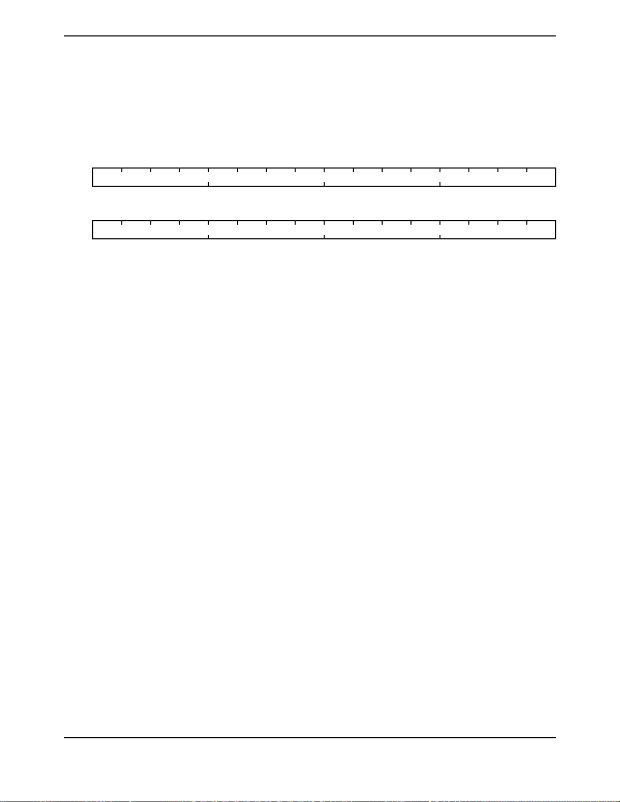
Register 14: Device Capabilities 0 (DC0), offset 0x008
This register is predefined by the part and can be used to verify features.
Device Capabilities 0 (DC0)
Base 0x400F.E000
Offset 0x008
Type RO, reset 0x001F.000F
SRAMSZ
FLASHSZ
DescriptionResetTypeNameBit/Field
LM3S617 Microcontroller
16171819202122232425262728293031
ROROROROROROROROROROROROROROROROType
1111100000000000Reset
0123456789101112131415
ROROROROROROROROROROROROROROROROType
1111000000000000Reset
0x001FROSRAMSZ31:16
SRAM Size
Indicates the size of the on-chip SRAM memory.
DescriptionValue
8 KB of SRAM0x001F
0x000FROFLASHSZ15:0
Flash Size
Indicates the size of the on-chip flash memory.
DescriptionValue
32 KB of Flash0x000F
Preliminary
81November 29, 2007

System Control
Register 15: Device Capabilities 1 (DC1), offset 0x010
This register provides a list of features available in the system. The Stellaris family uses this register
format to indicate the availability of the following family features in the specific device: PWM, ADC,
Watchdog timer, and debug capabilities. This register also indicates the maximum clock frequency
and maximum ADC sample rate. The format of this register is consistent with the RCGC0, SCGC0,
and DCGC0 clock control registers and the SRCR0 software reset control register.
Device Capabilities 1 (DC1)
Base 0x400F.E000
Offset 0x010
Type RO, reset 0x0011.32BF
16171819202122232425262728293031
ADCreservedPWMreserved
ROROROROROROROROROROROROROROROROType
1000100000000000Reset
0123456789101112131415
JTAGSWDSWOWDTPLLTEMPSNSreservedMPUMAXADCSPDMINSYSDIV
ROROROROROROROROROROROROROROROROType
1111110101001100Reset
DescriptionResetTypeNameBit/Field
0ROreserved31:21
Software should not rely on the value of a reserved bit. To provide
compatibility with future products, the value of a reserved bit should be
preserved across a read-modify-write operation.
1ROPWM20
PWM Module Present
When set, indicates that the PWM module is present.
0ROreserved19:17
Software should not rely on the value of a reserved bit. To provide
compatibility with future products, the value of a reserved bit should be
preserved across a read-modify-write operation.
1ROADC16
ADC Module Present
When set, indicates that the ADC module is present.
0x3ROMINSYSDIV15:12
System Clock Divider
Minimum 4-bit divider value for system clock. The reset value is
hardware-dependent. See the RCC register for how to change the
system clock divisor using the SYSDIV bit.
DescriptionValue
Specifies a 50-MHz CPU clock with a PLL divider of 4.0x3
0x2ROMAXADCSPD11:8
Max ADC Speed
Indicates the maximum rate at which the ADC samples data.
Preliminary
DescriptionValue
500K samples/second0x2
November 29, 200782

LM3S617 Microcontroller
DescriptionResetTypeNameBit/Field
1ROMPU7
0ROreserved6
1ROTEMPSNS5
1ROPLL4
1ROWDT3
1ROSWO2
1ROSWD1
MPU Present
When set, indicates that the Cortex-M3 Memory Protection Unit (MPU)
module is present. See the ARM Cortex-M3 Technical Reference Manual
for details on the MPU.
Software should not rely on the value of a reserved bit. To provide
compatibility with future products, the value of a reserved bit should be
preserved across a read-modify-write operation.
Temp Sensor Present
When set, indicates that the on-chip temperature sensor is present.
PLL Present
When set, indicates that the on-chip Phase Locked Loop (PLL) is
present.
Watchdog Timer Present
When set, indicates that a watchdog timer is present.
SWO Trace Port Present
When set, indicates that the Serial Wire Output (SWO) trace port is
present.
SWD Present
When set, indicates that the Serial Wire Debugger (SWD) is present.
1ROJTAG0
JTAG Present
When set, indicates that the JTAG debugger interface is present.
Preliminary
83November 29, 2007

System Control
Register 16: Device Capabilities 2 (DC2), offset 0x014
This register provides a list of features available in the system. The Stellaris family uses this register
format to indicate the availability of the following family features in the specific device: Analog
Comparators, General-Purpose Timers, I2Cs, QEIs, SSIs, and UARTs. The format of this register
is consistent with the RCGC1, SCGC1, and DCGC1 clock control registers and the SRCR1 software
reset control register.
Device Capabilities 2 (DC2)
Base 0x400F.E000
Offset 0x014
Type RO, reset 0x0107.0013
16171819202122232425262728293031
TIMER0TIMER1TIMER2reservedCOMP0reserved
ROROROROROROROROROROROROROROROROType
1110000010000000Reset
0123456789101112131415
UART0UART1reservedSSI0reserved
ROROROROROROROROROROROROROROROROType
1100100000000000Reset
DescriptionResetTypeNameBit/Field
0ROreserved31:25
Software should not rely on the value of a reserved bit. To provide
compatibility with future products, the value of a reserved bit should be
preserved across a read-modify-write operation.
1ROCOMP024
Analog Comparator 0 Present
When set, indicates that analog comparator 0 is present.
0ROreserved23:19
Software should not rely on the value of a reserved bit. To provide
compatibility with future products, the value of a reserved bit should be
preserved across a read-modify-write operation.
1ROTIMER218
Timer 2 Present
When set, indicates that General-Purpose Timer module 2 is present.
1ROTIMER117
Timer 1 Present
When set, indicates that General-Purpose Timer module 1 is present.
1ROTIMER016
Timer 0 Present
When set, indicates that General-Purpose Timer module 0 is present.
0ROreserved15:5
Software should not rely on the value of a reserved bit. To provide
compatibility with future products, the value of a reserved bit should be
preserved across a read-modify-write operation.
1ROSSI04
SSI0 Present
When set, indicates that SSI module 0 is present.
0ROreserved3:2
Preliminary
Software should not rely on the value of a reserved bit. To provide
compatibility with future products, the value of a reserved bit should be
preserved across a read-modify-write operation.
November 29, 200784

LM3S617 Microcontroller
DescriptionResetTypeNameBit/Field
1ROUART11
1ROUART00
UART1 Present
When set, indicates that UART module 1 is present.
UART0 Present
When set, indicates that UART module 0 is present.
Preliminary
85November 29, 2007

System Control
Register 17: Device Capabilities 3 (DC3), offset 0x018
This register provides a list of features available in the system. The Stellaris family uses this register
format to indicate the availability of the following family features in the specific device: Analog
Comparator I/Os, CCP I/Os, ADC I/Os, and PWM I/Os.
Device Capabilities 3 (DC3)
Base 0x400F.E000
Offset 0x018
Type RO, reset 0x3F3F.01FF
16171819202122232425262728293031
ADC0ADC1ADC2ADC3ADC4ADC5reservedCCP0CCP1CCP2CCP3CCP4CCP5reserved
ROROROROROROROROROROROROROROROROType
1111110011111100Reset
0123456789101112131415
PWM0PWM1PWM2PWM3PWM4PWM5C0MINUSC0PLUSC0Oreserved
ROROROROROROROROROROROROROROROROType
1111111110000000Reset
DescriptionResetTypeNameBit/Field
0ROreserved31:30
Software should not rely on the value of a reserved bit. To provide
compatibility with future products, the value of a reserved bit should be
preserved across a read-modify-write operation.
1ROCCP529
CCP5 Pin Present
When set, indicates that Capture/Compare/PWM pin 5 is present.
1ROCCP428
CCP4 Pin Present
When set, indicates that Capture/Compare/PWM pin 4 is present.
1ROCCP327
CCP3 Pin Present
When set, indicates that Capture/Compare/PWM pin 3 is present.
1ROCCP226
CCP2 Pin Present
When set, indicates that Capture/Compare/PWM pin 2 is present.
1ROCCP125
CCP1 Pin Present
When set, indicates that Capture/Compare/PWM pin 1 is present.
1ROCCP024
CCP0 Pin Present
When set, indicates that Capture/Compare/PWM pin 0 is present.
0ROreserved23:22
Software should not rely on the value of a reserved bit. To provide
compatibility with future products, the value of a reserved bit should be
preserved across a read-modify-write operation.
1ROADC521
1ROADC420
Preliminary
ADC5 Pin Present
When set, indicates that ADC pin 5 is present.
ADC4 Pin Present
When set, indicates that ADC pin 4 is present.
November 29, 200786

LM3S617 Microcontroller
DescriptionResetTypeNameBit/Field
1ROADC319
1ROADC218
1ROADC117
1ROADC016
0ROreserved15:9
1ROC0O8
1ROC0PLUS7
1ROC0MINUS6
ADC3 Pin Present
When set, indicates that ADC pin 3 is present.
ADC2 Pin Present
When set, indicates that ADC pin 2 is present.
ADC1 Pin Present
When set, indicates that ADC pin 1 is present.
ADC0 Pin Present
When set, indicates that ADC pin 0 is present.
Software should not rely on the value of a reserved bit. To provide
compatibility with future products, the value of a reserved bit should be
preserved across a read-modify-write operation.
C0o Pin Present
When set, indicates that the analog comparator 0 output pin is present.
C0+ Pin Present
When set, indicates that the analog comparator 0 (+) input pin is present.
C0- Pin Present
When set, indicates that the analog comparator 0 (-) input pin is present.
1ROPWM55
1ROPWM44
1ROPWM33
1ROPWM22
1ROPWM11
1ROPWM00
PWM5 Pin Present
When set, indicates that the PWM pin 5 is present.
PWM4 Pin Present
When set, indicates that the PWM pin 4 is present.
PWM3 Pin Present
When set, indicates that the PWM pin 3 is present.
PWM2 Pin Present
When set, indicates that the PWM pin 2 is present.
PWM1 Pin Present
When set, indicates that the PWM pin 1 is present.
PWM0 Pin Present
When set, indicates that the PWM pin 0 is present.
Preliminary
87November 29, 2007

System Control
Register 18: Device Capabilities 4 (DC4), offset 0x01C
This register provides a list of features available in the system. The Stellaris family uses this register
format to indicate the availability of GPIOs in the specific device. The format of this register is
consistent with the RCGC2, SCGC2, and DCGC2 clock control registers and the SRCR2 software
reset control register.
Device Capabilities 4 (DC4)
Base 0x400F.E000
Offset 0x01C
Type RO, reset 0x0000.001F
DescriptionResetTypeNameBit/Field
reserved
16171819202122232425262728293031
ROROROROROROROROROROROROROROROROType
0000000000000000Reset
0123456789101112131415
GPIOAGPIOBGPIOCGPIODGPIOEreserved
ROROROROROROROROROROROROROROROROType
1111100000000000Reset
0ROreserved31:5
Software should not rely on the value of a reserved bit. To provide
compatibility with future products, the value of a reserved bit should be
preserved across a read-modify-write operation.
1ROGPIOE4
GPIO Port E Present
When set, indicates that GPIO Port E is present.
1ROGPIOD3
GPIO Port D Present
When set, indicates that GPIO Port D is present.
1ROGPIOC2
GPIO Port C Present
When set, indicates that GPIO Port C is present.
1ROGPIOB1
GPIO Port B Present
When set, indicates that GPIO Port B is present.
1ROGPIOA0
GPIO Port A Present
When set, indicates that GPIO Port A is present.
Preliminary
November 29, 200788

Register 19: Run Mode Clock Gating Control Register 0 (RCGC0), offset 0x100
This register controls the clock gating logic. Each bit controls a clock enable for a given interface,
function, or unit. If set, the unit receives a clock and functions. Otherwise, the unit is unclocked and
disabled (saving power). If the unit is unclocked, reads or writes to the unit will generate a bus fault.
The reset state of these bits is 0 (unclocked) unless otherwise noted, so that all functional units are
disabled. It is the responsibility of software to enable the ports necessary for the application. Note
that these registers may contain more bits than there are interfaces, functions, or units to control.
This is to assure reasonable code compatibility with other family and future parts. RCGC0 is the
clock configuration register for running operation, SCGC0 for Sleep operation, and DCGC0 for
Deep-Sleep operation. Setting the ACG bit in the Run-Mode Clock Configuration (RCC) register
specifies that the system uses sleep modes.
Run Mode Clock Gating Control Register 0 (RCGC0)
Base 0x400F.E000
Offset 0x100
Type R/W, reset 0x00000040
LM3S617 Microcontroller
16171819202122232425262728293031
ADCreservedPWMreserved
R/WROROROR/WROROROROROROROROROROROType
0000000000000000Reset
0123456789101112131415
reservedWDTreservedMAXADCSPDreserved
ROROROR/WROROROROR/WR/WR/WR/WROROROROType
0000000000000000Reset
DescriptionResetTypeNameBit/Field
0ROreserved31:21
0R/WPWM20
0ROreserved19:17
0R/WADC16
0ROreserved15:12
Software should not rely on the value of a reserved bit. To provide
compatibility with future products, the value of a reserved bit should be
preserved across a read-modify-write operation.
PWM Clock Gating Control
This bit controls the clock gating for the PWM module. If set, the unit
receives a clock and functions. Otherwise, the unit is unclocked and
disabled. If the unit is unclocked, a read or write to the unit generates
a bus fault.
Software should not rely on the value of a reserved bit. To provide
compatibility with future products, the value of a reserved bit should be
preserved across a read-modify-write operation.
ADC0 Clock Gating Control
This bit controls the clock gating for SAR ADC module 0. If set, the unit
receives a clock and functions. Otherwise, the unit is unclocked and
disabled. If the unit is unclocked, a read or write to the unit generates
a bus fault.
Software should not rely on the value of a reserved bit. To provide
compatibility with future products, the value of a reserved bit should be
preserved across a read-modify-write operation.
Preliminary
89November 29, 2007

System Control
DescriptionResetTypeNameBit/Field
0R/WMAXADCSPD11:8
0ROreserved7:4
0R/WWDT3
0ROreserved2:0
ADC Sample Speed
This field sets the rate at which the ADC samples data. You cannot set
the rate higher than the maximum rate. You can set the sample rate by
setting the MAXADCSPD bit as follows:
DescriptionValue
500K samples/second0x2
250K samples/second0x1
125K samples/second0x0
Software should not rely on the value of a reserved bit. To provide
compatibility with future products, the value of a reserved bit should be
preserved across a read-modify-write operation.
WDT Clock Gating Control
This bit controls the clock gating for the WDT module. If set, the unit
receives a clock and functions. Otherwise, the unit is unclocked and
disabled. If the unit is unclocked, a read or write to the unit generates
a bus fault.
Software should not rely on the value of a reserved bit. To provide
compatibility with future products, the value of a reserved bit should be
preserved across a read-modify-write operation.
Preliminary
November 29, 200790
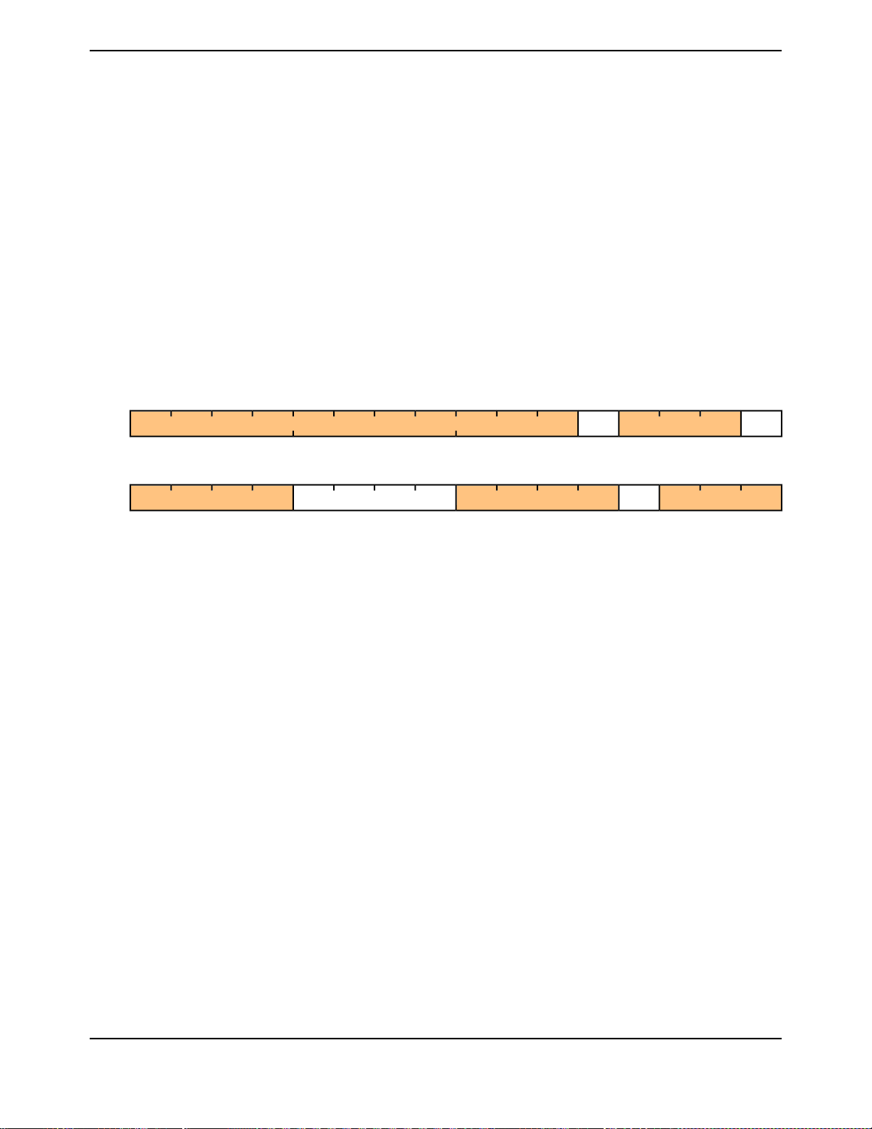
Register 20: Sleep Mode Clock Gating Control Register 0 (SCGC0), offset 0x110
This register controls the clock gating logic. Each bit controls a clock enable for a given interface,
function, or unit. If set, the unit receives a clock and functions. Otherwise, the unit is unclocked and
disabled (saving power). If the unit is unclocked, reads or writes to the unit will generate a bus fault.
The reset state of these bits is 0 (unclocked) unless otherwise noted, so that all functional units are
disabled. It is the responsibility of software to enable the ports necessary for the application. Note
that these registers may contain more bits than there are interfaces, functions, or units to control.
This is to assure reasonable code compatibility with other family and future parts. RCGC0 is the
clock configuration register for running operation, SCGC0 for Sleep operation, and DCGC0 for
Deep-Sleep operation. Setting the ACG bit in the Run-Mode Clock Configuration (RCC) register
specifies that the system uses sleep modes.
Sleep Mode Clock Gating Control Register 0 (SCGC0)
Base 0x400F.E000
Offset 0x110
Type R/W, reset 0x00000040
LM3S617 Microcontroller
16171819202122232425262728293031
ADCreservedPWMreserved
R/WROROROR/WROROROROROROROROROROROType
0000000000000000Reset
0123456789101112131415
reservedWDTreservedMAXADCSPDreserved
ROROROR/WROROROROR/WR/WR/WR/WROROROROType
0000000000000000Reset
DescriptionResetTypeNameBit/Field
0ROreserved31:21
0R/WPWM20
0ROreserved19:17
0R/WADC16
0ROreserved15:12
Software should not rely on the value of a reserved bit. To provide
compatibility with future products, the value of a reserved bit should be
preserved across a read-modify-write operation.
PWM Clock Gating Control
This bit controls the clock gating for the PWM module. If set, the unit
receives a clock and functions. Otherwise, the unit is unclocked and
disabled. If the unit is unclocked, a read or write to the unit generates
a bus fault.
Software should not rely on the value of a reserved bit. To provide
compatibility with future products, the value of a reserved bit should be
preserved across a read-modify-write operation.
ADC0 Clock Gating Control
This bit controls the clock gating for SAR ADC module 0. If set, the unit
receives a clock and functions. Otherwise, the unit is unclocked and
disabled. If the unit is unclocked, a read or write to the unit generates
a bus fault.
Software should not rely on the value of a reserved bit. To provide
compatibility with future products, the value of a reserved bit should be
preserved across a read-modify-write operation.
Preliminary
91November 29, 2007

System Control
DescriptionResetTypeNameBit/Field
0R/WMAXADCSPD11:8
0ROreserved7:4
0R/WWDT3
0ROreserved2:0
ADC Sample Speed
This field sets the rate at which the ADC samples data. You cannot set
the rate higher than the maximum rate. You can set the sample rate by
setting the MAXADCSPD bit as follows:
DescriptionValue
500K samples/second0x2
250K samples/second0x1
125K samples/second0x0
Software should not rely on the value of a reserved bit. To provide
compatibility with future products, the value of a reserved bit should be
preserved across a read-modify-write operation.
WDT Clock Gating Control
This bit controls the clock gating for the WDT module. If set, the unit
receives a clock and functions. Otherwise, the unit is unclocked and
disabled. If the unit is unclocked, a read or write to the unit generates
a bus fault.
Software should not rely on the value of a reserved bit. To provide
compatibility with future products, the value of a reserved bit should be
preserved across a read-modify-write operation.
Preliminary
November 29, 200792

Register 21: Deep Sleep Mode Clock Gating Control Register 0 (DCGC0), offset 0x120
This register controls the clock gating logic. Each bit controls a clock enable for a given interface,
function, or unit. If set, the unit receives a clock and functions. Otherwise, the unit is unclocked and
disabled (saving power). If the unit is unclocked, reads or writes to the unit will generate a bus fault.
The reset state of these bits is 0 (unclocked) unless otherwise noted, so that all functional units are
disabled. It is the responsibility of software to enable the ports necessary for the application. Note
that these registers may contain more bits than there are interfaces, functions, or units to control.
This is to assure reasonable code compatibility with other family and future parts. RCGC0 is the
clock configuration register for running operation, SCGC0 for Sleep operation, and DCGC0 for
Deep-Sleep operation. Setting the ACG bit in the Run-Mode Clock Configuration (RCC) register
specifies that the system uses sleep modes.
Deep Sleep Mode Clock Gating Control Register 0 (DCGC0)
Base 0x400F.E000
Offset 0x120
Type R/W, reset 0x00000040
LM3S617 Microcontroller
16171819202122232425262728293031
ADCreservedPWMreserved
R/WROROROR/WROROROROROROROROROROROType
0000000000000000Reset
0123456789101112131415
reservedWDTreservedMAXADCSPDreserved
ROROROR/WROROROROR/WR/WR/WR/WROROROROType
0000000000000000Reset
DescriptionResetTypeNameBit/Field
0ROreserved31:21
0R/WPWM20
0ROreserved19:17
0R/WADC16
0ROreserved15:12
Software should not rely on the value of a reserved bit. To provide
compatibility with future products, the value of a reserved bit should be
preserved across a read-modify-write operation.
PWM Clock Gating Control
This bit controls the clock gating for the PWM module. If set, the unit
receives a clock and functions. Otherwise, the unit is unclocked and
disabled. If the unit is unclocked, a read or write to the unit generates
a bus fault.
Software should not rely on the value of a reserved bit. To provide
compatibility with future products, the value of a reserved bit should be
preserved across a read-modify-write operation.
ADC0 Clock Gating Control
This bit controls the clock gating for SAR ADC module 0. If set, the unit
receives a clock and functions. Otherwise, the unit is unclocked and
disabled. If the unit is unclocked, a read or write to the unit generates
a bus fault.
Software should not rely on the value of a reserved bit. To provide
compatibility with future products, the value of a reserved bit should be
preserved across a read-modify-write operation.
Preliminary
93November 29, 2007

System Control
DescriptionResetTypeNameBit/Field
0R/WMAXADCSPD11:8
0ROreserved7:4
0R/WWDT3
0ROreserved2:0
ADC Sample Speed
This field sets the rate at which the ADC samples data. You cannot set
the rate higher than the maximum rate. You can set the sample rate by
setting the MAXADCSPD bit as follows:
DescriptionValue
500K samples/second0x2
250K samples/second0x1
125K samples/second0x0
Software should not rely on the value of a reserved bit. To provide
compatibility with future products, the value of a reserved bit should be
preserved across a read-modify-write operation.
WDT Clock Gating Control
This bit controls the clock gating for the WDT module. If set, the unit
receives a clock and functions. Otherwise, the unit is unclocked and
disabled. If the unit is unclocked, a read or write to the unit generates
a bus fault.
Software should not rely on the value of a reserved bit. To provide
compatibility with future products, the value of a reserved bit should be
preserved across a read-modify-write operation.
Preliminary
November 29, 200794
Register 22: Run Mode Clock Gating Control Register 1 (RCGC1), offset 0x104
This register controls the clock gating logic. Each bit controls a clock enable for a given interface,
function, or unit. If set, the unit receives a clock and functions. Otherwise, the unit is unclocked and
disabled (saving power). If the unit is unclocked, reads or writes to the unit will generate a bus fault.
The reset state of these bits is 0 (unclocked) unless otherwise noted, so that all functional units are
disabled. It is the responsibility of software to enable the ports necessary for the application. Note
that these registers may contain more bits than there are interfaces, functions, or units to control.
This is to assure reasonable code compatibility with other family and future parts. RCGC1 is the
clock configuration register for running operation, SCGC1 for Sleep operation, and DCGC1 for
Deep-Sleep operation. Setting the ACG bit in the Run-Mode Clock Configuration (RCC) register
specifies that the system uses sleep modes.
Run Mode Clock Gating Control Register 1 (RCGC1)
Base 0x400F.E000
Offset 0x104
Type R/W, reset 0x00000000
LM3S617 Microcontroller
16171819202122232425262728293031
TIMER0TIMER1TIMER2reservedCOMP0reserved
R/WR/WR/WROROROROROR/WROROROROROROROType
0000000000000000Reset
0123456789101112131415
UART0UART1reservedSSI0reserved
R/WR/WROROR/WROROROROROROROROROROROType
0000000000000000Reset
DescriptionResetTypeNameBit/Field
0ROreserved31:25
0R/WCOMP024
0ROreserved23:19
0R/WTIMER218
0R/WTIMER117
Software should not rely on the value of a reserved bit. To provide
compatibility with future products, the value of a reserved bit should be
preserved across a read-modify-write operation.
Analog Comparator 0 Clock Gating
This bit controls the clock gating for analog comparator 0. If set, the unit
receives a clock and functions. Otherwise, the unit is unclocked and
disabled. If the unit is unclocked, reads or writes to the unit will generate
a bus fault.
Software should not rely on the value of a reserved bit. To provide
compatibility with future products, the value of a reserved bit should be
preserved across a read-modify-write operation.
Timer 2 Clock Gating Control
This bit controls the clock gating for General-Purpose Timer module 2.
If set, the unit receives a clock and functions. Otherwise, the unit is
unclocked and disabled. If the unit is unclocked, reads or writes to the
unit will generate a bus fault.
Timer 1 Clock Gating Control
This bit controls the clock gating for General-Purpose Timer module 1.
If set, the unit receives a clock and functions. Otherwise, the unit is
unclocked and disabled. If the unit is unclocked, reads or writes to the
unit will generate a bus fault.
Preliminary
95November 29, 2007

System Control
DescriptionResetTypeNameBit/Field
0R/WTIMER016
0ROreserved15:5
0R/WSSI04
0ROreserved3:2
0R/WUART11
0R/WUART00
Timer 0 Clock Gating Control
This bit controls the clock gating for General-Purpose Timer module 0.
If set, the unit receives a clock and functions. Otherwise, the unit is
unclocked and disabled. If the unit is unclocked, reads or writes to the
unit will generate a bus fault.
Software should not rely on the value of a reserved bit. To provide
compatibility with future products, the value of a reserved bit should be
preserved across a read-modify-write operation.
SSI0 Clock Gating Control
This bit controls the clock gating for SSI module 0. If set, the unit receives
a clock and functions. Otherwise, the unit is unclocked and disabled. If
the unit is unclocked, reads or writes to the unit will generate a bus fault.
Software should not rely on the value of a reserved bit. To provide
compatibility with future products, the value of a reserved bit should be
preserved across a read-modify-write operation.
UART1 Clock Gating Control
This bit controls the clock gating for UART module 1. If set, the unit
receives a clock and functions. Otherwise, the unit is unclocked and
disabled. If the unit is unclocked, reads or writes to the unit will generate
a bus fault.
UART0 Clock Gating Control
This bit controls the clock gating for UART module 0. If set, the unit
receives a clock and functions. Otherwise, the unit is unclocked and
disabled. If the unit is unclocked, reads or writes to the unit will generate
a bus fault.
Preliminary
November 29, 200796

Register 23: Sleep Mode Clock Gating Control Register 1 (SCGC1), offset 0x114
This register controls the clock gating logic. Each bit controls a clock enable for a given interface,
function, or unit. If set, the unit receives a clock and functions. Otherwise, the unit is unclocked and
disabled (saving power). If the unit is unclocked, reads or writes to the unit will generate a bus fault.
The reset state of these bits is 0 (unclocked) unless otherwise noted, so that all functional units are
disabled. It is the responsibility of software to enable the ports necessary for the application. Note
that these registers may contain more bits than there are interfaces, functions, or units to control.
This is to assure reasonable code compatibility with other family and future parts. RCGC1 is the
clock configuration register for running operation, SCGC1 for Sleep operation, and DCGC1 for
Deep-Sleep operation. Setting the ACG bit in the Run-Mode Clock Configuration (RCC) register
specifies that the system uses sleep modes.
Sleep Mode Clock Gating Control Register 1 (SCGC1)
Base 0x400F.E000
Offset 0x114
Type R/W, reset 0x00000000
LM3S617 Microcontroller
16171819202122232425262728293031
TIMER0TIMER1TIMER2reservedCOMP0reserved
R/WR/WR/WROROROROROR/WROROROROROROROType
0000000000000000Reset
0123456789101112131415
UART0UART1reservedSSI0reserved
R/WR/WROROR/WROROROROROROROROROROROType
0000000000000000Reset
DescriptionResetTypeNameBit/Field
0ROreserved31:25
0R/WCOMP024
0ROreserved23:19
0R/WTIMER218
0R/WTIMER117
Software should not rely on the value of a reserved bit. To provide
compatibility with future products, the value of a reserved bit should be
preserved across a read-modify-write operation.
Analog Comparator 0 Clock Gating
This bit controls the clock gating for analog comparator 0. If set, the unit
receives a clock and functions. Otherwise, the unit is unclocked and
disabled. If the unit is unclocked, reads or writes to the unit will generate
a bus fault.
Software should not rely on the value of a reserved bit. To provide
compatibility with future products, the value of a reserved bit should be
preserved across a read-modify-write operation.
Timer 2 Clock Gating Control
This bit controls the clock gating for General-Purpose Timer module 2.
If set, the unit receives a clock and functions. Otherwise, the unit is
unclocked and disabled. If the unit is unclocked, reads or writes to the
unit will generate a bus fault.
Timer 1 Clock Gating Control
This bit controls the clock gating for General-Purpose Timer module 1.
If set, the unit receives a clock and functions. Otherwise, the unit is
unclocked and disabled. If the unit is unclocked, reads or writes to the
unit will generate a bus fault.
Preliminary
97November 29, 2007

System Control
DescriptionResetTypeNameBit/Field
0R/WTIMER016
0ROreserved15:5
0R/WSSI04
0ROreserved3:2
0R/WUART11
0R/WUART00
Timer 0 Clock Gating Control
This bit controls the clock gating for General-Purpose Timer module 0.
If set, the unit receives a clock and functions. Otherwise, the unit is
unclocked and disabled. If the unit is unclocked, reads or writes to the
unit will generate a bus fault.
Software should not rely on the value of a reserved bit. To provide
compatibility with future products, the value of a reserved bit should be
preserved across a read-modify-write operation.
SSI0 Clock Gating Control
This bit controls the clock gating for SSI module 0. If set, the unit receives
a clock and functions. Otherwise, the unit is unclocked and disabled. If
the unit is unclocked, reads or writes to the unit will generate a bus fault.
Software should not rely on the value of a reserved bit. To provide
compatibility with future products, the value of a reserved bit should be
preserved across a read-modify-write operation.
UART1 Clock Gating Control
This bit controls the clock gating for UART module 1. If set, the unit
receives a clock and functions. Otherwise, the unit is unclocked and
disabled. If the unit is unclocked, reads or writes to the unit will generate
a bus fault.
UART0 Clock Gating Control
This bit controls the clock gating for UART module 0. If set, the unit
receives a clock and functions. Otherwise, the unit is unclocked and
disabled. If the unit is unclocked, reads or writes to the unit will generate
a bus fault.
Preliminary
November 29, 200798

Register 24: Deep Sleep Mode Clock Gating Control Register 1 (DCGC1), offset 0x124
This register controls the clock gating logic. Each bit controls a clock enable for a given interface,
function, or unit. If set, the unit receives a clock and functions. Otherwise, the unit is unclocked and
disabled (saving power). If the unit is unclocked, reads or writes to the unit will generate a bus fault.
The reset state of these bits is 0 (unclocked) unless otherwise noted, so that all functional units are
disabled. It is the responsibility of software to enable the ports necessary for the application. Note
that these registers may contain more bits than there are interfaces, functions, or units to control.
This is to assure reasonable code compatibility with other family and future parts. RCGC1 is the
clock configuration register for running operation, SCGC1 for Sleep operation, and DCGC1 for
Deep-Sleep operation. Setting the ACG bit in the Run-Mode Clock Configuration (RCC) register
specifies that the system uses sleep modes.
Deep Sleep Mode Clock Gating Control Register 1 (DCGC1)
Base 0x400F.E000
Offset 0x124
Type R/W, reset 0x00000000
LM3S617 Microcontroller
16171819202122232425262728293031
TIMER0TIMER1TIMER2reservedCOMP0reserved
R/WR/WR/WROROROROROR/WROROROROROROROType
0000000000000000Reset
0123456789101112131415
UART0UART1reservedSSI0reserved
R/WR/WROROR/WROROROROROROROROROROROType
0000000000000000Reset
DescriptionResetTypeNameBit/Field
0ROreserved31:25
0R/WCOMP024
0ROreserved23:19
0R/WTIMER218
0R/WTIMER117
Software should not rely on the value of a reserved bit. To provide
compatibility with future products, the value of a reserved bit should be
preserved across a read-modify-write operation.
Analog Comparator 0 Clock Gating
This bit controls the clock gating for analog comparator 0. If set, the unit
receives a clock and functions. Otherwise, the unit is unclocked and
disabled. If the unit is unclocked, reads or writes to the unit will generate
a bus fault.
Software should not rely on the value of a reserved bit. To provide
compatibility with future products, the value of a reserved bit should be
preserved across a read-modify-write operation.
Timer 2 Clock Gating Control
This bit controls the clock gating for General-Purpose Timer module 2.
If set, the unit receives a clock and functions. Otherwise, the unit is
unclocked and disabled. If the unit is unclocked, reads or writes to the
unit will generate a bus fault.
Timer 1 Clock Gating Control
This bit controls the clock gating for General-Purpose Timer module 1.
If set, the unit receives a clock and functions. Otherwise, the unit is
unclocked and disabled. If the unit is unclocked, reads or writes to the
unit will generate a bus fault.
Preliminary
99November 29, 2007

System Control
DescriptionResetTypeNameBit/Field
0R/WTIMER016
0ROreserved15:5
0R/WSSI04
0ROreserved3:2
0R/WUART11
0R/WUART00
Timer 0 Clock Gating Control
This bit controls the clock gating for General-Purpose Timer module 0.
If set, the unit receives a clock and functions. Otherwise, the unit is
unclocked and disabled. If the unit is unclocked, reads or writes to the
unit will generate a bus fault.
Software should not rely on the value of a reserved bit. To provide
compatibility with future products, the value of a reserved bit should be
preserved across a read-modify-write operation.
SSI0 Clock Gating Control
This bit controls the clock gating for SSI module 0. If set, the unit receives
a clock and functions. Otherwise, the unit is unclocked and disabled. If
the unit is unclocked, reads or writes to the unit will generate a bus fault.
Software should not rely on the value of a reserved bit. To provide
compatibility with future products, the value of a reserved bit should be
preserved across a read-modify-write operation.
UART1 Clock Gating Control
This bit controls the clock gating for UART module 1. If set, the unit
receives a clock and functions. Otherwise, the unit is unclocked and
disabled. If the unit is unclocked, reads or writes to the unit will generate
a bus fault.
UART0 Clock Gating Control
This bit controls the clock gating for UART module 0. If set, the unit
receives a clock and functions. Otherwise, the unit is unclocked and
disabled. If the unit is unclocked, reads or writes to the unit will generate
a bus fault.
Preliminary
November 29, 2007100
 Loading...