

Page 1
SJ1 SJ1
Connects SoftStart Capacitor
Connects Tracking
Resistors
AN-1573 LM2745-19A Demonstration Board
1 Introduction
This application notes describes the LM2745 printed circuit board (PCB) design and provides an example
typical application circuit. The LM2745 is a voltage mode PWM buck controller which implements
synchronous rectification. It provides a low cost, high power density, and efficient point of load solution. In
steady state operation the LM2745 is always synchronous, even at no load, thus simplifying the
compensation design. The LM2745 ensures a smooth and controlled start-up when the output is prebiased. The current limit protection does not require a current limit resistor in the power path, but is
achieved by sensing the voltage VDSacross the low side MOSFET. Though the control sections of the IC
are rated for 3 to 6V (VCC), the driver sections are designed to accept input supply rails (VIN) as high as
14V.
2 Specifics Of The Board
This demo board targets the fixed and mobile telecommunications, industrial electronics, and distributed
power markets. The demo board has a VINrange of 8V to 14V and a LDO regulator, the LP2937, powers
VCCby regulating a 5V output voltage. The LM2745 regulates to an output range of 1.2V to 3.3V at 19A
with a switching frequency of 300 kHz. Note, the demo board is optimized for the above parameters, thus
for additional design modifications refer to the Design Consideration section of the LM2745 data sheet.
The PCB is designed on four layers, the top and bottom layers are 2oz. copper and the two inner layers
are 1oz. copper. The board measures 2.19 in. x 1.03 in. x 0.41 in. (56 mm x 26.2 mm x 10.3 mm) (l, w, h)
on a FR4 laminate.
User's Guide
SNVA213A–May 2007–Revised May 2013
3 Feature Options
When the tracking feature of the LM2745 is required for use, remove the jumper that connects the softstart capacitor C10 and connect the resistor divider, on designators R13 and R14 (see Figure 1). The
Track terminal has been provided for your connecting convenience. The demo board is synchronize ready,
just connect an external clock to the SYNC terminal. Note: increasing the switching frequency results in a
lower inductor current ripple and input and output voltage ripple (if the component values are kept the
same). Monitor the MOSFET junction temperature since switching losses will increase, and do not exceed
the maximum junction temperature of the MOSFET. Refer to the MOSFET manufacturer datasheet for
maximum junction temperature specification and heat sinking guidelines.
Figure 1. Soft-Start and Tracking Jumper
All trademarks are the property of their respective owners.
SNVA213A–May 2007–Revised May 2013 AN-1573 LM2745-19A Demonstration Board
Submit Documentation Feedback
1
Copyright © 2007–2013, Texas Instruments Incorporated
Page 2

Specification Summary
4 Specification Summary
• Space saving footprint
• Wide ambient temperature range: -40 ºC to 65 ºC
• Input voltage range: 8V to 14V
• Adjustable output voltage: 1.2V to 3.3V
• No minimum load requirement
• Remote ON/OFF
• Power good signal
• Fixed switching frequency: 300 kHz
• Switching frequency synchronize range 250 kHz to 1 MHz
• Current Limit Protection
• Master power supply start-up tracking function
• Start-up with a pre-biased output load
• Adjustable soft-start
• Small size 2.19 in. x 1.03 in. x 0.41 in. (56 mm x 26.2 mm x 10.3 mm)
5 Performance Characteristics
Efficiency
www.ti.com
2
AN-1573 LM2745-19A Demonstration Board SNVA213A–May 2007–Revised May 2013
Figure 2. Efficiency vs. Load Current
V
= 3.3V, fSW= 300 kHz
OUT
Copyright © 2007–2013, Texas Instruments Incorporated
Submit Documentation Feedback
Page 3
www.ti.com
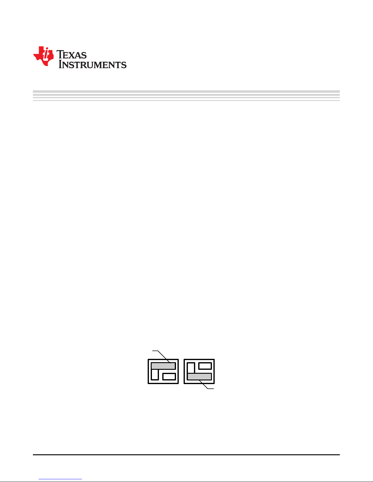
6 Switch Node Voltage and Output Voltage Ripple
Switch Node Voltage and Output Voltage Ripple
Figure 3. VIN= 8V, V
I
= 100 mA, fSW= 300 kHz
LOAD
OUT
20 MHz Bandwidth Limit
Figure 4. VIN= 8V, V
I
= 19A, fSW= 300 kHz
LOAD
OUT
20 MHz Bandwidth Limit
= 3.3V,
= 3.3V,
SNVA213A–May 2007–Revised May 2013 AN-1573 LM2745-19A Demonstration Board
Submit Documentation Feedback
3
Copyright © 2007–2013, Texas Instruments Incorporated
Page 4

Switch Node Voltage and Output Voltage Ripple
www.ti.com
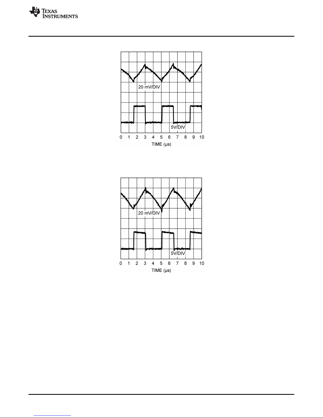
Figure 5. VIN= 14V, V
I
= 100 mA, fSW= 300 kHz
LOAD
20 MHz Bandwidth Limit
Figure 6. VIN= 14V, V
I
= 19A, fSW= 300 kHz
LOAD
20 MHz Bandwidth Limit
OUT
OUT
= 3.3V,
= 3.3V,
4
AN-1573 LM2745-19A Demonstration Board SNVA213A–May 2007–Revised May 2013
Copyright © 2007–2013, Texas Instruments Incorporated
Submit Documentation Feedback
Page 5
100 µs/DIV
50 mV/DIV
5A/DIV
100 µs/DIV
50 mV/DIV
2A/DIV
www.ti.com
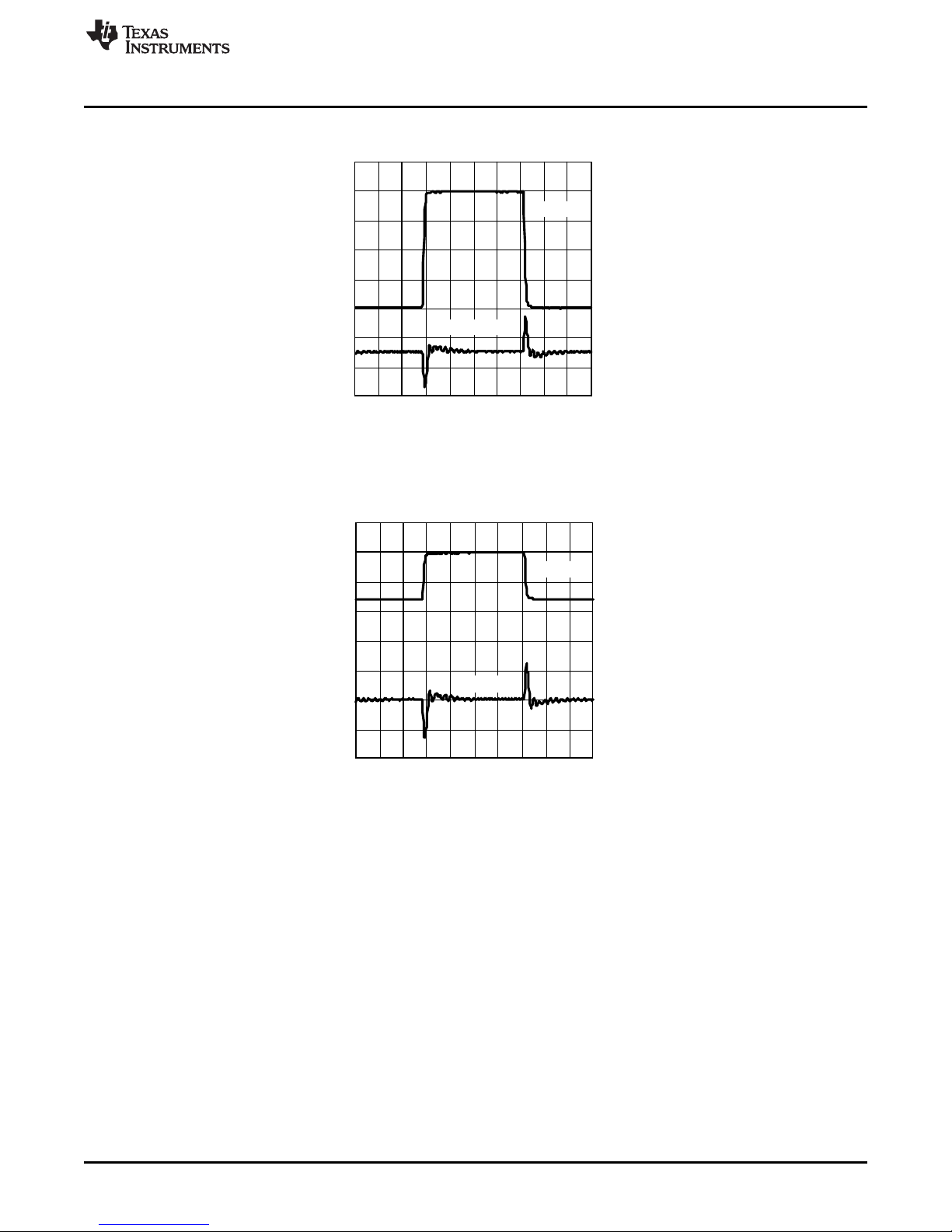
7 Load Transient Response
Load Transient Response
Figure 7. VIN= 14V, V
I
= 2A to 10A
LOAD
CH1: V
, CH2: I
OUT
Figure 8. VIN= 14V, V
I
= 11A to 19A
LOAD
CH1: V
, CH2: I
OUT
OUT
LOAD
OUT
LOAD
= 3.3V
= 3.3V
SNVA213A–May 2007–Revised May 2013 AN-1573 LM2745-19A Demonstration Board
Submit Documentation Feedback
5
Copyright © 2007–2013, Texas Instruments Incorporated
Page 6
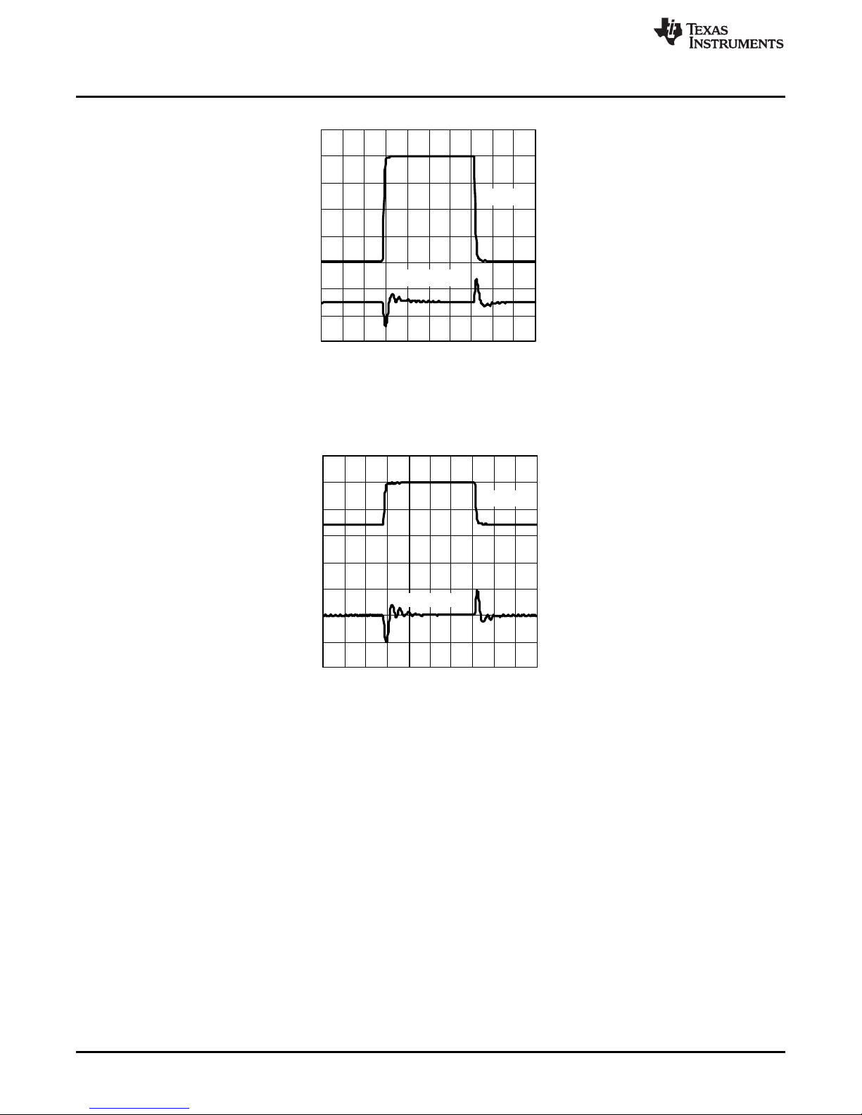
100 µs/DIV
100 mV/DIV
5A/DIV
100 µs/DIV
100 mV/DIV
2A/DIV
Load Transient Response
www.ti.com
Figure 9. VIN= 8V, V
I
= 2A to 10A
LOAD
CH1: V
, CH2: I
OUT
Figure 10. VIN= 8V, V
I
= 11A to 19A
LOAD
CH1: V
, CH2: I
OUT
OUT
OUT
= 3.3V
LOAD
= 3.3V
LOAD
6
AN-1573 LM2745-19A Demonstration Board SNVA213A–May 2007–Revised May 2013
Copyright © 2007–2013, Texas Instruments Incorporated
Submit Documentation Feedback
Page 7
www.ti.com
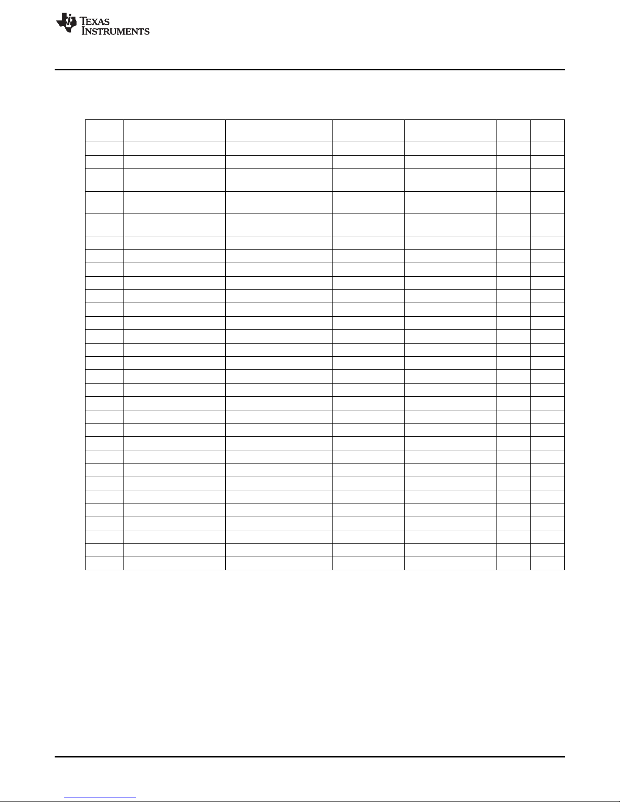
8 Bill of Materials
Table 1. Bill of Materials for LM2745 POL EVB (Vin: 8V to 14V, Vout:3.3V, 19A)
Locatio Part Number Type Size Parameters Qty Vendo
n r
U1 LM2745 Syn. Buck Controller TSSOP-14 Vin: 4.5V - 5.5V 1 NSC
U2 LM27937IMP-5.0 Linear Regulator 5V,500mA SOT-223 5V, 500mA 1 NSC
L1 SER2010-202ML Inductor 2uH, 27A, 0.852mohm 1 Coilcraf
Q1-2 IRF6633 N-MOSFET DirectFET-MP 20V, 16A, 4.1mohm, 2 Vishay
Q3 IRF6609 N-MOSFET DirectFET-MT 20V, 150A, 2mohm, 1 Vishay
D1 SL22-E3/2C Schottky Diode SMB 20V, 2A 1 Vishay
D2 MBRS0520 Schottky Diode SOD123 20V, 0.5A 1 Vishay
C1, 2 GRM32ER61C226KE20L Ceramic Capacitor 1210 22µF, 25V, X7R, 5% 2 Murata
C3, 11 GRM319R71H104KA01B Ceramic Capacitor 1206 100nF, 25V, X7R, 10% 2 Murata
C14 GRM319R71H474KA01B Ceramic Capacitor 1206 470nF, 25V, X7R, 10% 1 Murata
C9 GRM1885C1H1210JA01 Ceramic Capacitor 0603 120pF, 50V, C0G, 5% 1 Murata
C6 GRM188R71H222KA01 Ceramic Capacitor 0603 2.2nF, 50V, X7R, 10% 1 Murata
C7 GRM1885C1H101JA01 Ceramic Capacitor 0603 100pF, 50V, C0G, 5% 1 Murata
C8 GRM188R71H332KA01 Ceramic Capacitor 0603 3.3nF, 50V, X7R, 10% 1 Murata
C10 GRM188R71H153KA01 Ceramic Capacitor 0603 15nF, 50V, X7R, 10% 1 Murata
C12 GRM40X7R472K25 Ceramic Capacitor 0805 470nF, 25V, X7R, 10% 1 Murata
C13 12066D226MAT Ceramic Capacitor 1206 22µF, 6.3V, X5R, 20% 1 AVX
C4, 5 6SVPC220M OS-CON C6 220µF, 6.3V, 20% 2 Sanyo
R1,18 CRCW06030R00F Chip Resistor 0603 0ohm 2 Vishay
R2 CRCW06032151F Chip Resistor 0603 2.15k, 1% 1 Vishay
R3, R17 CRCW06031002F Chip Resistor 0603 10k, 1% 2 Vishay
R4 CRCW06032211F Chip Resistor 0603 2.21k, 1% 1 Vishay
R10, 11 CRCW06031003F Chip Resistor 0603 100k, 1% 2 Vishay
R5, 6, 8 CRCW06032R21F Chip Resistor 0603 2.21ohm, 1% 3 Vishay
R7, 9 CRCW06034702F Chip Resistor 0603 47k, 1% 2 Vishay
R12 CRCW06038451F Chip Resistor 0603 8.45k, 1% 1 Vishay
R15 CRCW06031821F Chip Resistor 0603 1.82k, 1% 1 Vishay
R16 CRCW060310R0F Chip Resistor 0603 10ohm, 1% 1 Vishay
- - F-Pin 8
- - Pin 90 deg., SIP, 6 way Pitch: 2.54mm 1
Bill of Materials
t
11nC
46nC
SNVA213A–May 2007–Revised May 2013 AN-1573 LM2745-19A Demonstration Board
Submit Documentation Feedback
7
Copyright © 2007–2013, Texas Instruments Incorporated
Page 8

R3
C8
R12
R15
C10
R10
C11
D2
C14
C2
L1
+
C9
R4
C5
R2
C6
R17
+
C4
C1
R11
Q1
R16
+
C3
VIN
Q3
HG
BOO
T
LG
PGND
FB
PWGD
FREQ/SYNC
SS/TRACK
SGND
EAO
PGND
LM2745
V
OUT
LM2937
V
IN
C13
V
OUT
GND
C12
D1
Q2
SD
R6
R5
R7
R8
R9
R18
U1
U2
C7
SYNC
R14
R13
TRACK
SJ2
PWGD
SD
TRIM
SENSE
SJ1
V
CC
I
SEN
PCB Layout
www.ti.com
9 PCB Layout
Figure 11. 300 kHz Demo Board Schematic
Figure 12. Top Silkscreen
8
AN-1573 LM2745-19A Demonstration Board SNVA213A–May 2007–Revised May 2013
Copyright © 2007–2013, Texas Instruments Incorporated
Submit Documentation Feedback
Page 9

www.ti.com
PCB Layout
Figure 13. Top Copper Layer
Figure 14. Bottom Silkscreen
Figure 15. Bottom Copper Layer
SNVA213A–May 2007–Revised May 2013 AN-1573 LM2745-19A Demonstration Board
Submit Documentation Feedback
9
Copyright © 2007–2013, Texas Instruments Incorporated
Page 10

PCB Layout
www.ti.com
Figure 16. Internal Layer-1 (GND Copper)
Figure 17. Internal Layer-2 (GND Copper)
10
AN-1573 LM2745-19A Demonstration Board SNVA213A–May 2007–Revised May 2013
Copyright © 2007–2013, Texas Instruments Incorporated
Submit Documentation Feedback
Page 11

IMPORTANT NOTICE
Texas Instruments Incorporated and its subsidiaries (TI) reserve the right to make corrections, enhancements, improvements and other
changes to its semiconductor products and services per JESD46, latest issue, and to discontinue any product or service per JESD48, latest
issue. Buyers should obtain the latest relevant information before placing orders and should verify that such information is current and
complete. All semiconductor products (also referred to herein as “components”) are sold subject to TI’s terms and conditions of sale
supplied at the time of order acknowledgment.
TI warrants performance of its components to the specifications applicable at the time of sale, in accordance with the warranty in TI’s terms
and conditions of sale of semiconductor products. Testing and other quality control techniques are used to the extent TI deems necessary
to support this warranty. Except where mandated by applicable law, testing of all parameters of each component is not necessarily
performed.
TI assumes no liability for applications assistance or the design of Buyers’ products. Buyers are responsible for their products and
applications using TI components. To minimize the risks associated with Buyers’ products and applications, Buyers should provide
adequate design and operating safeguards.
TI does not warrant or represent that any license, either express or implied, is granted under any patent right, copyright, mask work right, or
other intellectual property right relating to any combination, machine, or process in which TI components or services are used. Information
published by TI regarding third-party products or services does not constitute a license to use such products or services or a warranty or
endorsement thereof. Use of such information may require a license from a third party under the patents or other intellectual property of the
third party, or a license from TI under the patents or other intellectual property of TI.
Reproduction of significant portions of TI information in TI data books or data sheets is permissible only if reproduction is without alteration
and is accompanied by all associated warranties, conditions, limitations, and notices. TI is not responsible or liable for such altered
documentation. Information of third parties may be subject to additional restrictions.
Resale of TI components or services with statements different from or beyond the parameters stated by TI for that component or service
voids all express and any implied warranties for the associated TI component or service and is an unfair and deceptive business practice.
TI is not responsible or liable for any such statements.
Buyer acknowledges and agrees that it is solely responsible for compliance with all legal, regulatory and safety-related requirements
concerning its products, and any use of TI components in its applications, notwithstanding any applications-related information or support
that may be provided by TI. Buyer represents and agrees that it has all the necessary expertise to create and implement safeguards which
anticipate dangerous consequences of failures, monitor failures and their consequences, lessen the likelihood of failures that might cause
harm and take appropriate remedial actions. Buyer will fully indemnify TI and its representatives against any damages arising out of the use
of any TI components in safety-critical applications.
In some cases, TI components may be promoted specifically to facilitate safety-related applications. With such components, TI’s goal is to
help enable customers to design and create their own end-product solutions that meet applicable functional safety standards and
requirements. Nonetheless, such components are subject to these terms.
No TI components are authorized for use in FDA Class III (or similar life-critical medical equipment) unless authorized officers of the parties
have executed a special agreement specifically governing such use.
Only those TI components which TI has specifically designated as military grade or “enhanced plastic” are designed and intended for use in
military/aerospace applications or environments. Buyer acknowledges and agrees that any military or aerospace use of TI components
which have not been so designated is solely at the Buyer's risk, and that Buyer is solely responsible for compliance with all legal and
regulatory requirements in connection with such use.
TI has specifically designated certain components as meeting ISO/TS16949 requirements, mainly for automotive use. In any case of use of
non-designated products, TI will not be responsible for any failure to meet ISO/TS16949.
Products Applications
Audio www.ti.com/audio Automotive and Transportation www.ti.com/automotive
Amplifiers amplifier.ti.com Communications and Telecom www.ti.com/communications
Data Converters dataconverter.ti.com Computers and Peripherals www.ti.com/computers
DLP® Products www.dlp.com Consumer Electronics www.ti.com/consumer-apps
DSP dsp.ti.com Energy and Lighting www.ti.com/energy
Clocks and Timers www.ti.com/clocks Industrial www.ti.com/industrial
Interface interface.ti.com Medical www.ti.com/medical
Logic logic.ti.com Security www.ti.com/security
Power Mgmt power.ti.com Space, Avionics and Defense www.ti.com/space-avionics-defense
Microcontrollers microcontroller.ti.com Video and Imaging www.ti.com/video
RFID www.ti-rfid.com
OMAP Applications Processors www.ti.com/omap TI E2E Community e2e.ti.com
Wireless Connectivity www.ti.com/wirelessconnectivity
Mailing Address: Texas Instruments, Post Office Box 655303, Dallas, Texas 75265
Copyright © 2013, Texas Instruments Incorporated
Page 12

Mouser Electronics
Authorized Distributor
Click to View Pricing, Inventory, Delivery & Lifecycle Information:
Texas Instruments:
LM2745-19AEVAL
 Loading...