

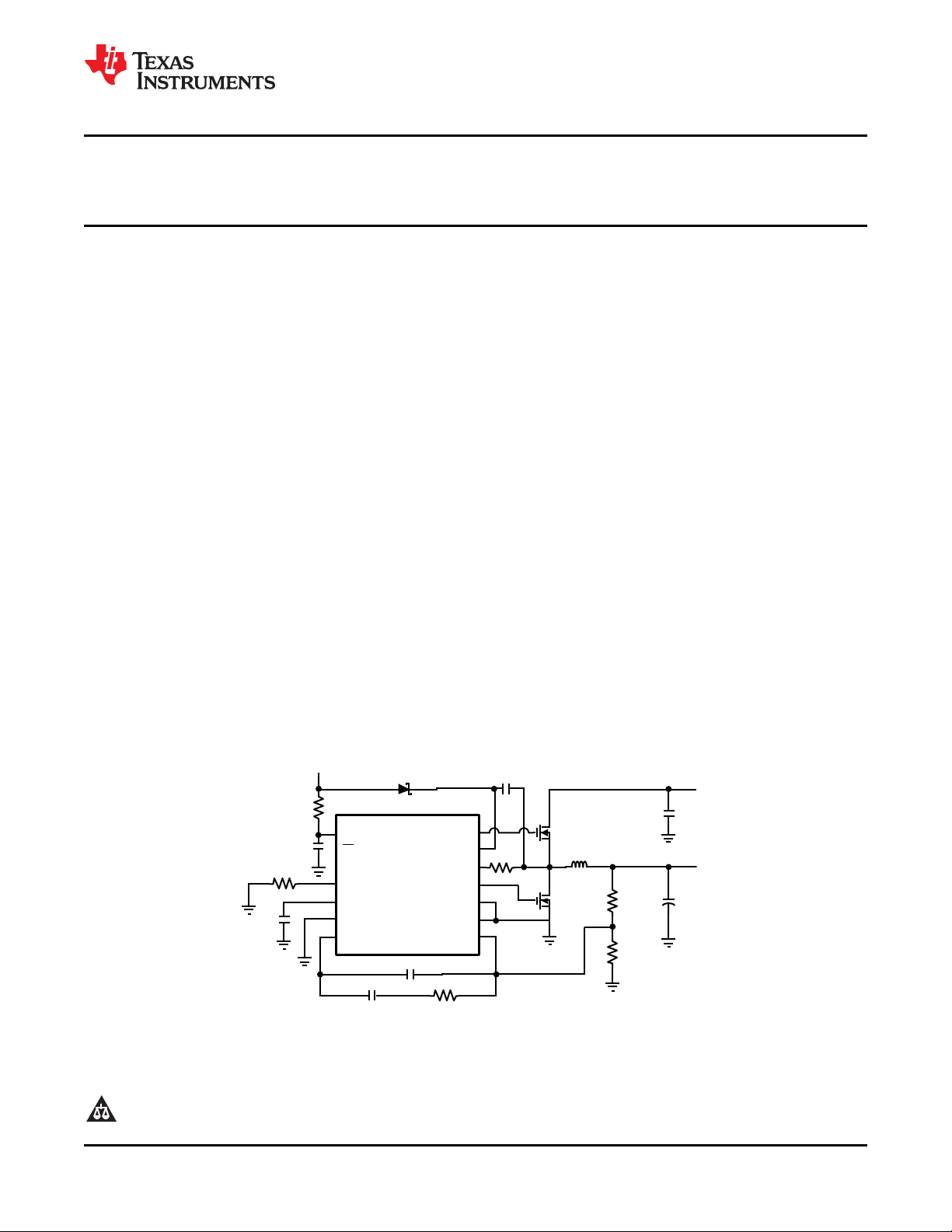
LM27x7
HG
BOOT
I
SEN
LG
PGND
FB
V
CC
SD
PWGD
FREQ
SS
SGND
EAO
PGND
+5V
VIN = 3.3V
VO = 1.2V@5A
CO1,2
2200PF
6.3V, 2.8A
1.5 PH
6.1 A, 9.6 m:
R
FB2
C
C2
R
C1
R
CS
C
SS
R
FADJ
R
IN
C
IN
D1
C
BOOT
Q1
Q2
10PF
6.3V
10k
2.2k
10k
392k
2.2p
180p
12n
63.4k
2.2PF
10:
0.1P
CIN1,2
L1
+
C
C1
R
FB1
Si4884DY
Si4884DY
LM2727, LM2737
www.ti.com
SNVS205D –AUGUST 2002–REVISED MARCH 2013
LM2727/LM2737 N-Channel FET Synchronous Buck Regulator Controller for Low Output
Voltages
Check for Samples: LM2727, LM2737
1
FEATURES
2
• Input Power from 2.2V to 16V
• Output Voltage Adjustable Down to 0.6V
• Power Good flag, Adjustable Soft-Start and
Output Enable for Easy Power Sequencing
• Output Over-Voltage and Under-Voltage LatchOff (LM2727)
• Output Over-Voltage and Under-Voltage Flag
(LM2737)
• Reference Accuracy: 1.5% (0°C - 125°C)
• Current Limit Without Sense Resistor
• Soft Start
• Switching Frequency from 50 kHz to 2 MHz adjusting the value of an external resistor. Current
• TSSOP-14 Package
APPLICATIONS
• Cable Modems
• Set-Top Boxes/ Home Gateways
• DDR Core Power
• High-Efficiency Distributed Power
• Local Regulation of Core Power
DESCRIPTION
The LM2727 and LM2737 are high-speed,
synchronous, switching regulator controllers. They
are intended to control currents of 0.7A to 20A with
up to 95% conversion efficiencies. The LM2727
employs output over-voltage and under-voltage latchoff. For applications where latch-off is not desired, the
LM2737 can be used. Power up and down
sequencing is achieved with the power-good flag,
adjustable soft-start and output enable features. The
LM2737 and LM2737 operate from a low-current 5V
bias and can convert from a 2.2V to 16V power rail.
Both parts utilize a fixed-frequency, voltage-mode,
PWM control architecture and the switching
frequency is adjustable from 50kHz to 2MHz by
limit is achieved by monitoring the voltage drop
across the on-resistance of the low-side MOSFET,
which enhances low duty-cycle operation. The wide
range of operating frequencies gives the power
supply designer the flexibility to fine-tune component
size, cost, noise and efficiency. The adaptive, nonoverlapping MOSFET gate-drivers and high-side
bootstrap structure helps to further maximize
efficiency. The high-side power FET drain voltage can
be from 2.2V to 16V and the output voltage is
adjustable down to 0.6V.
Typical Application
1
2All trademarks are the property of their respective owners.
PRODUCTION DATA information is current as of publication date.
Products conform to specifications per the terms of the Texas
Instruments standard warranty. Production processing does not
necessarily include testing of all parameters.
Please be aware that an important notice concerning availability, standard warranty, and use in critical applications of
Texas Instruments semiconductor products and disclaimers thereto appears at the end of this data sheet.
Copyright © 2002–2013, Texas Instruments Incorporated
LM27x7
HG
BOOT
ISEN
LG
PGND
FB
Vcc
SD
PWGD
FREQ
SS
SGND
EAO
PGND
1
2
3
4
5
6
7 8
9
10
11
12
13
14
LM2727, LM2737
SNVS205D –AUGUST 2002–REVISED MARCH 2013
www.ti.com
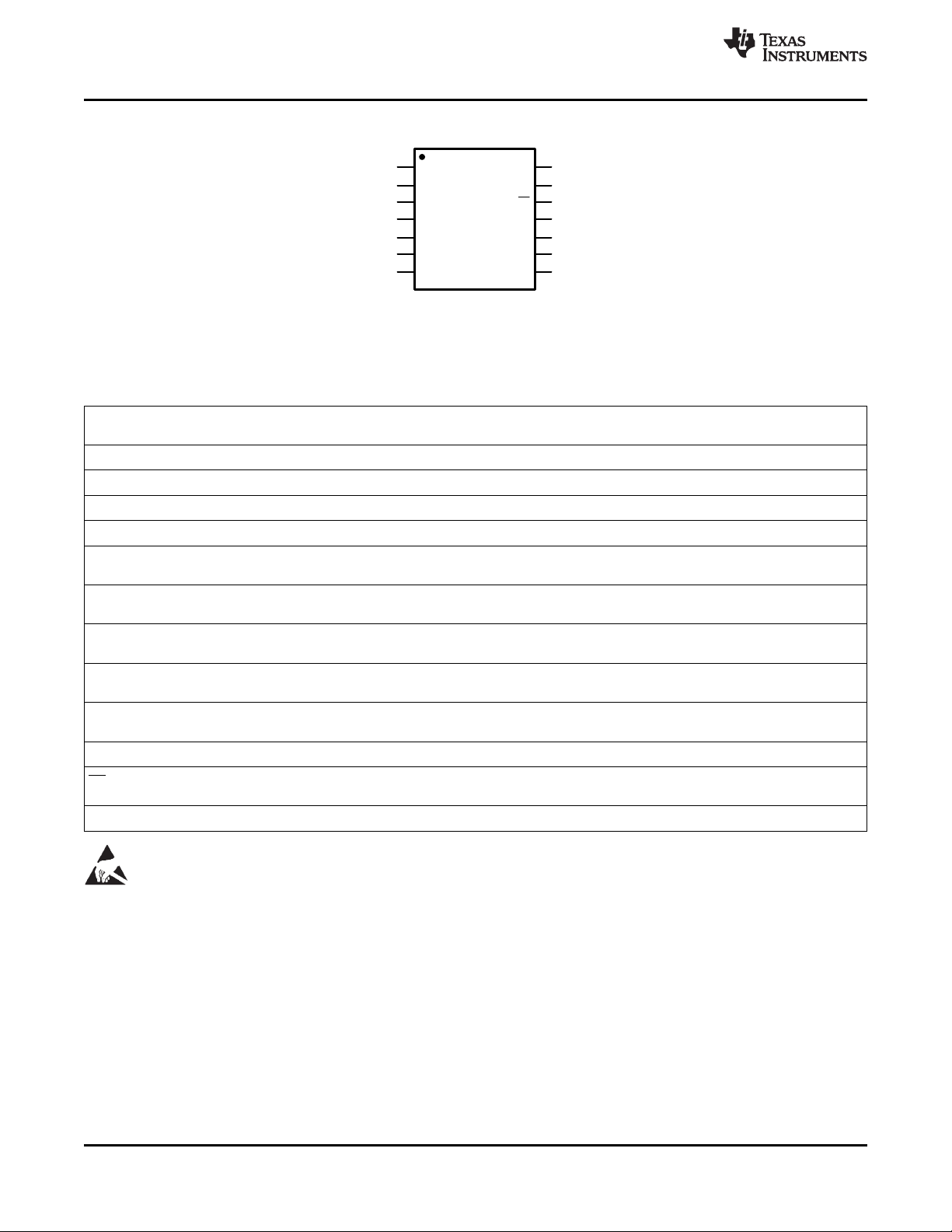
Connection Diagram
Figure 1. 14-Lead Plastic TSSOP
θ
= 155°C/W
See Package Number PW0014A
BOOT (Pin 1) - Supply rail for the N-channel MOSFET gate drive. The voltage should be at least one gate threshold above the regulator
input voltage to properly turn on the high-side N-FET.
LG (Pin 2) - Gate drive for the low-side N-channel MOSFET. This signal is interlocked with HG to avoid shoot-through problems.
PGND (Pins 3, 13) - Ground for FET drive circuitry. It should be connected to system ground.
SGND (Pin 4) - Ground for signal level circuitry. It should be connected to system ground.
VCC(Pin 5) - Supply rail for the controller.
PWGD (Pin 6) - Power Good. This is an open drain output. The pin is pulled low when the chip is in UVP, OVP, or UVLO mode. During
normal operation, this pin is connected to VCCor other voltage source through a pull-up resistor.
ISEN (Pin 7) - Current limit threshold setting. This sources a fixed 50µA current. A resistor of appropriate value should be connected
between this pin and the drain of the low-side FET.
EAO (Pin 8) - Output of the error amplifier. The voltage level on this pin is compared with an internally generated ramp signal to determine
the duty cycle. This pin is necessary for compensating the control loop.
SS (Pin 9) - Soft start pin. A capacitor connected between this pin and ground sets the speed at which the output voltage ramps up. Larger
capacitor value results in slower output voltage ramp but also lower inrush current.
FB (Pin 10) - This is the inverting input of the error amplifier, which is used for sensing the output voltage and compensating the control
loop.
FREQ (Pin 11) - The switching frequency is set by connecting a resistor between this pin and ground.
SD (Pin 12) - IC Logic Shutdown. When this pin is pulled low the chip turns off the high side switch and turns on the low side switch. While
this pin is low, the IC will not start up. An internal 20µA pull-up connects this pin to VCC.
HG (Pin 14) - Gate drive for the high-side N-channel MOSFET. This signal is interlocked with LG to avoid shoot-through problems.
JA
PIN DESCRIPTION
2 Submit Documentation Feedback Copyright © 2002–2013, Texas Instruments Incorporated
These devices have limited built-in ESD protection. The leads should be shorted together or the device placed in conductive foam
during storage or handling to prevent electrostatic damage to the MOS gates.
Product Folder Links: LM2727 LM2737
LM2727, LM2737
www.ti.com
Absolute Maximum Ratings
V
CC
(1)(2)
SNVS205D –AUGUST 2002–REVISED MARCH 2013
BOOTV 21V
Junction Temperature 150°C
Storage Temperature −65°C to 150°C
Soldering Information
Lead Temperature (soldering, 10sec) 260°C
Infrared or Convection (20sec) 235°C
ESD Rating
(3)
2 kV
(1) Absolute maximum ratings indicate limits beyond which damage to the device may occur. Operating ratings indicate conditions for
which the device operates correctly. Opearting Ratings do not imply ensured performance limits.
(2) If Military/Aerospace specified devices are required, please contact the Texas Instruments Sales Office/ Distributors for availability and
specifications.
(3) The human body model is a 100pF capacitor discharged through a 1.5k resistor into each pin.
Operating Ratings
Supply Voltage (VCC) 4.5V to 5.5V
Junction Temperature Range −40°C to +125°C
Thermal Resistance (θJA) 155°C/W
Electrical Characteristics
VCC= 5V unless otherwise indicated. Typicals and limits appearing in plain type apply for TA=TJ=+25°C. Limits appearing in
boldface type apply over full Operating Temperature Range. Datasheet min/max specification limits are ensured by design,
test, or statistical analysis.
Symbol Parameter Conditions Min Typ Max Units
VCC= 4.5V, 0°C to +125°C 0.591 0.6 0.609
VCC= 5V, 0°C to +125°C 0.591 0.6 0.609
V
FB_ADJ
V
I
Q-V5
t
PWGD1
t
PWGD2
I
I
SS-ON
I
SS-OC
I
SEN-TH
SD
ON
FB Pin Voltage V
UVLO Thresholds Rising 4.2
Operating VCCCurrent mA
Shutdown VCCCurrent SD = 0V 0.15 0.4 0.7 mA
PWGD Pin Response Time FB Voltage Going Up 6 µs
PWGD Pin Response Time FB Voltage Going Down 6 µs
SD Pin Internal Pull-up Current 20 µA
SS Pin Source Current SS Voltage = 2.5V
SS Pin Sink Current During Over SS Voltage = 2.5V
Current
I
Pin Source Current Trip Point 0°C to +125°C 35 50 65
SEN
VCC= 5.5V, 0°C to +125°C 0.591 0.6 0.609
VCC= 4.5V, −40°C to +125°C 0.589 0.6 0.609
VCC= 5V, −40°C to +125°C 0.589 0.6 0.609
VCC= 5.5V, −40°C to +125°C 0.589 0.6 0.609
Falling 3.6
SD = 5V, FB = 0.55V
Fsw = 600kHz
SD = 5V, FB = 0.65V
Fsw = 600kHz
1 1.5 2
0.8 1.7 2.2
0°C to +125°C 8 11 15 µA
-40°C to +125°C 5 11 15
95 µA
-40°C to +125°C 28 50 65
µA
V
7V
Copyright © 2002–2013, Texas Instruments Incorporated Submit Documentation Feedback 3
Product Folder Links: LM2727 LM2737
LM2727, LM2737
SNVS205D –AUGUST 2002–REVISED MARCH 2013
www.ti.com
Electrical Characteristics (continued)
VCC= 5V unless otherwise indicated. Typicals and limits appearing in plain type apply for TA=TJ=+25°C. Limits appearing in
boldface type apply over full Operating Temperature Range. Datasheet min/max specification limits are ensured by design,
test, or statistical analysis.
Symbol Parameter Conditions Min Typ Max Units
ERROR AMPLIFIER
GBW Error Amplifier Unity Gain
Bandwidth
G Error Amplifier DC Gain 60 dB
SR Error Amplifier Slew Rate 6 V/µA
I
I
EAO
V
FB
EA
FB Pin Bias Current FB = 0.55V 0 15 100
FB = 0.65V 0 30 155
EAO Pin Current Sourcing and V
Sinking V
= 2.5, FB = 0.55V 2.8
EAO
= 2.5, FB = 0.65V 0.8
EAO
Error Amplifier Maximum Swing Minimum 1.2
Maximum 3.2
GATE DRIVE
I
Q-BOOT
BOOT Pin Quiescent Current BOOTV = 12V, EN = 0
0°C to +125°C 95 160 µA
-40°C to +125°C 95 215
R
DS1
R
DS2
R
DS3
R
DS4
Top FET Driver Pull-Up ON
resistance
Top FET Driver Pull-Down ON
resistance
Bottom FET Driver Pull-Up ON
resistance
Bottom FET Driver Pull-Down ON
resistance
BOOT-SW = 5V@350mA 3 Ω
BOOT-SW = 5V@350mA 2 Ω
BOOT-SW = 5V@350mA 3 Ω
BOOT-SW = 5V@350mA 2 Ω
OSCILLATOR
R
= 590kΩ 50
FADJ
R
= 88.7kΩ 300
FADJ
R
= 42.2kΩ, 0°C to +125°C 500 600 700
f
OSC
PWM Frequency kHz
D Max Duty Cycle f
FADJ
R
= 42.2kΩ, -40°C to +125°C 490 600 700
FADJ
R
= 17.4kΩ 1400
FADJ
R
= 11.3kΩ 2000
FADJ
= 300kHz 90 %
PWM
f
= 600kHz 88
PWM
LOGIC INPUTS AND OUTPUTS
V
SD-IH
V
SD-IL
V
PWGD-TH-LO
SD Pin Logic High Trip Point 2.6 3.5 V
SD Pin Logic Low Trip Point 0°C to +125°C 1.3 1.6
-40°C to +125°C 1.25 1.6
PWGD Pin Trip Points FB Voltage Going Down
0°C to +125°C 0.413 0.430 0.446 V
-40°C to +125°C 0.410 0.430 0.446
V
PWGD-TH-HI
PWGD Pin Trip Points FB Voltage Going Up
0°C to +125°C 0.691 0.710 0.734 V
-40°C to +125°C 0.688 0.710 0.734
V
PWGD-HYS
PWGD Hysteresis (LM2737 only) FB Voltage Going Down FB Voltage 35
Going Up 110
5 MHz
nA
mA
V
V
mV
4 Submit Documentation Feedback Copyright © 2002–2013, Texas Instruments Incorporated
Product Folder Links: LM2727 LM2737
PWM FREQUENCY (kHz)
612
614
616
618
620
622
624
626
628
630
AMBIENT TEMPERATURE (oC)
0
10
20
25
35
45
55
65
75
85
95
105
115
125
7
7.2
7.4
7.6
7.8
8
8.2
8.4
8.6
BOOT PIN CURRENT (mA)
AMBIENT TEMPERATURE (oC)
0
10
20
25
35
45
55
65
75
85
95
105
115
125
AMBIENT TEMPERATURE (oC)
OPEARTING CURRENT(mA)
0 20
35
55
75
95
115
Without
Bootstrap
(V
boot
= 12V)
With
Bootstrap
(V
boot
= 5V)
1.46
1.48
1.5
1.52
1.54
1.56
1.58
1.6
1.62
1.64
BOOT PIN CURRENT (mA)
28.9
29.1
29.3
29.5
29.7
29.9
30.1
30.3
AMBIENT TEMPERATURE (oC)
0 10
20
25
35
45
55
65
75
85
95
105
115
125
20
30
40
50
60
70
80
90
100
0.2
1
3 5
7
9
OUTPUT CURRENT (A)
EFFICIENCY (%)
Vin = 5V
Vin = 12V
Vin = 3.3V
30
40
50
60
70
80
90
100
0.1 0.5
2
4
6
8
10
Vin = 5V
Vin = 12V
OUTPUT CURRENT (A)
EFFICIENCY (%)
LM2727, LM2737
www.ti.com
SNVS205D –AUGUST 2002–REVISED MARCH 2013
Typical Performance Characteristics
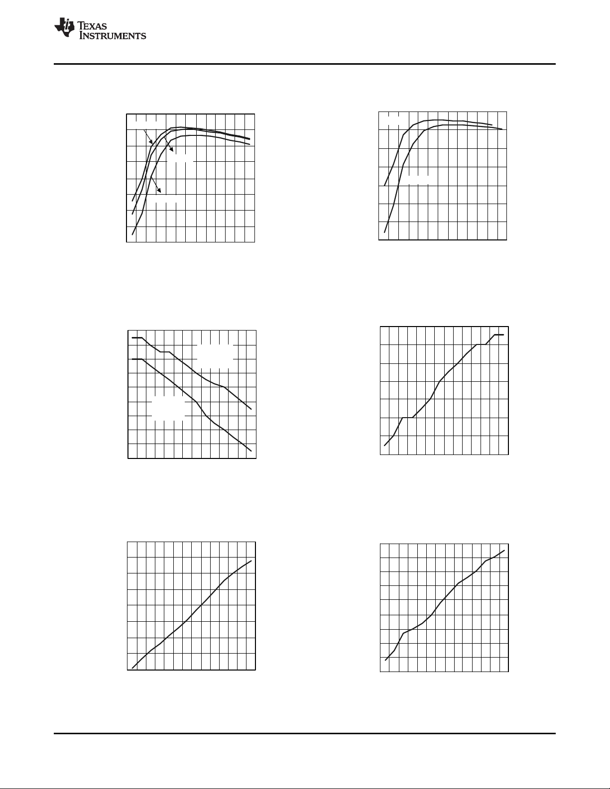
Efficiency (VO= 1.5V) Efficiency (VO= 3.3V)
FSW= 300kHz, TA= 25°C FSW= 300kHz, TA= 25°C
Figure 2. Figure 3.
VCCOperating Current Bootpin Current
FSW= 600kHz, No-Load FSW= 600kHz, Si4826DY FET, No-Load
vs vs
Temperature Temperature for BOOTV = 12V
Figure 4. Figure 5.
Bootpin Current PWM Frequency
vs vs
= 43.2kΩ
FADJ
Figure 6. Figure 7.
Temperature with 5V Bootstrap Temperature
FSW= 600kHz, Si4826DY FET, No-Load for R
Copyright © 2002–2013, Texas Instruments Incorporated Submit Documentation Feedback 5
Product Folder Links: LM2727 LM2737
V
CC
PLUS BOOT CURRENT
0
5
10
15
20
25
30
35
40
100300 500 700 90011001300150017001900
PWM FREQUENCY (kHz)
10
15
20
25
30
900
1000
11001200
1300
1400
1500
1600
1700
1800
1900
PWM FREQUENCY (kHz)
RF-ADJ (k:)
PWM FREQUENCY (kHz)
RF-ADJ (k:)
0
100
200
300
400
500
100 150
200
250
300350400
450
500600
700
800
LM2727, LM2737
SNVS205D –AUGUST 2002–REVISED MARCH 2013
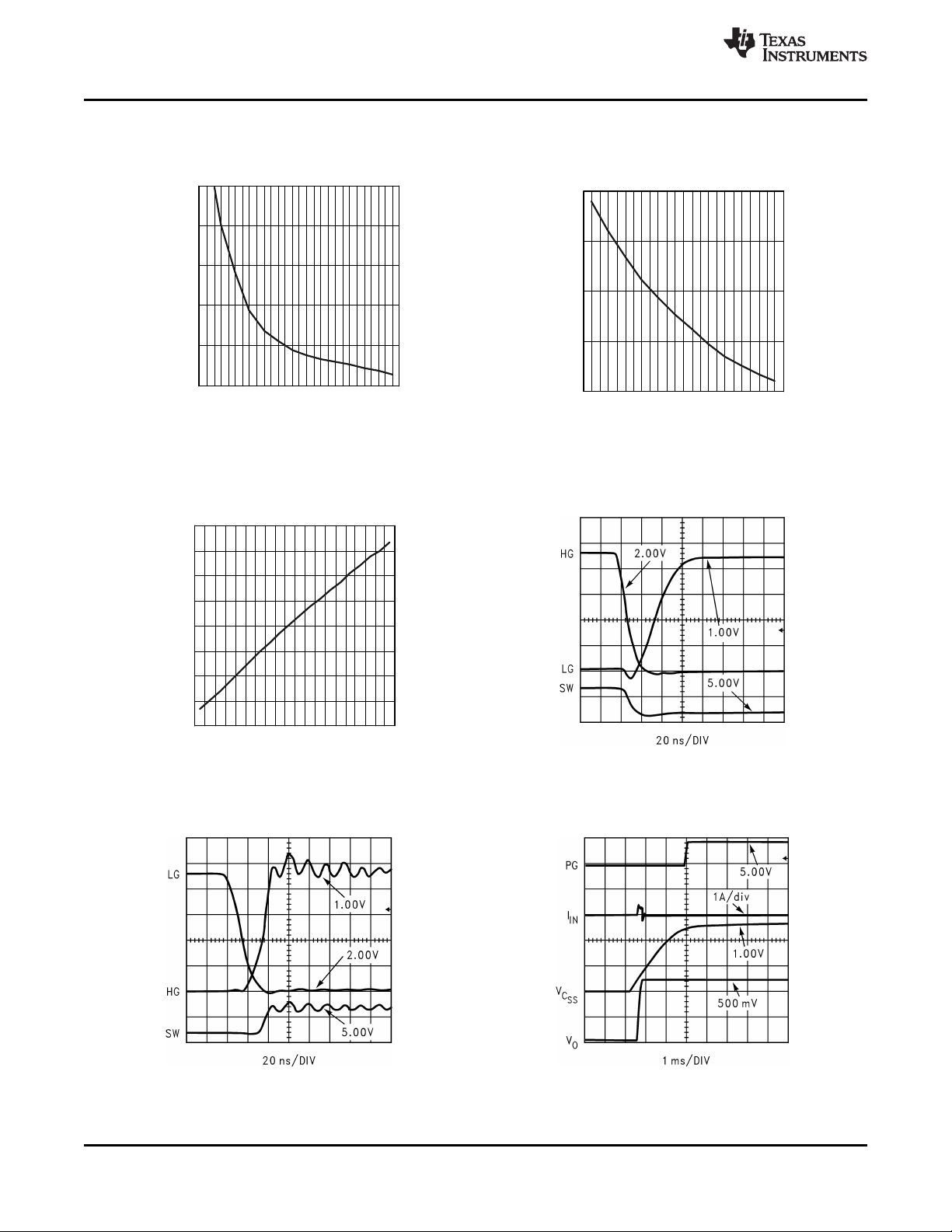
Typical Performance Characteristics (continued)
R
FADJ
vs vs
(in 100 to 800kHz range), TA= 25°C (in 900 to 2000kHz range), TA= 25°C
VCCOperating Current Plus Boot Current vs IO= 3A, CSS= 10nF
PWM Frequency (Si4826DY FET, TA= 25°C) FSW= 600kHz
PWM Frequency PWM Frequency
Figure 8. Figure 9.
R
FADJ
Switch Waveforms (HG Falling)
VIN= 5V, VO= 1.8V
www.ti.com
6 Submit Documentation Feedback Copyright © 2002–2013, Texas Instruments Incorporated
Figure 10. Figure 11.
Switch Waveforms (HG Rising) Start-Up (No-Load)
VIN= 5V, VO= 1.8V VIN= 10V, VO= 1.2V
IO= 3A, FSW= 600kHz CSS= 10nF, FSW= 300kHz
Figure 12. Figure 13.
Product Folder Links: LM2727 LM2737
LM2727, LM2737
www.ti.com
SNVS205D –AUGUST 2002–REVISED MARCH 2013
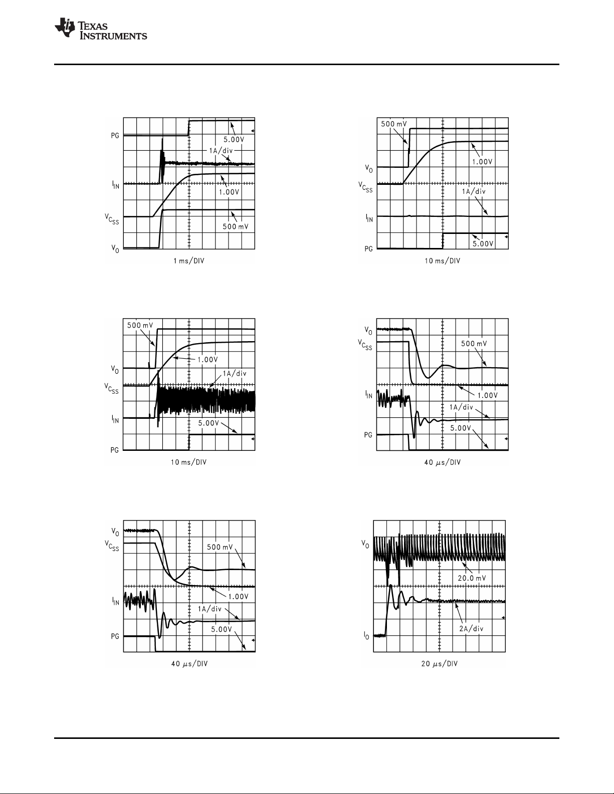
Typical Performance Characteristics (continued)
Start-Up (Full-Load)
VIN= 10V, VO= 1.2V Start Up (No-Load, 10x CSS)
IO= 10A, CSS= 10nF VIN= 10V, VO= 1.2V
FSW= 300kHz CSS= 100nF, FSW= 300kHz
Figure 14. Figure 15.
Start Up (Full Load, 10x CSS) Shutdown
VIN= 10V, VO= 1.2V VIN= 10V, VO= 1.2V
IO= 10A, CSS= 100nF IO= 10A, CSS= 10nF
FSW= 300kHz FSW= 300kHz
Figure 16. Figure 17.
Start Up (Full Load, 10x CSS)
VIN= 10V, VO= 1.2V Load Transient Response (IO= 0 to 4A)
IO= 10A, CSS= 100nF VIN= 12V, VO= 1.2V
FSW= 300kHz FSW= 300kHz
Figure 18. Figure 19.
Copyright © 2002–2013, Texas Instruments Incorporated Submit Documentation Feedback 7
Product Folder Links: LM2727 LM2737
LM2727, LM2737
SNVS205D –AUGUST 2002–REVISED MARCH 2013
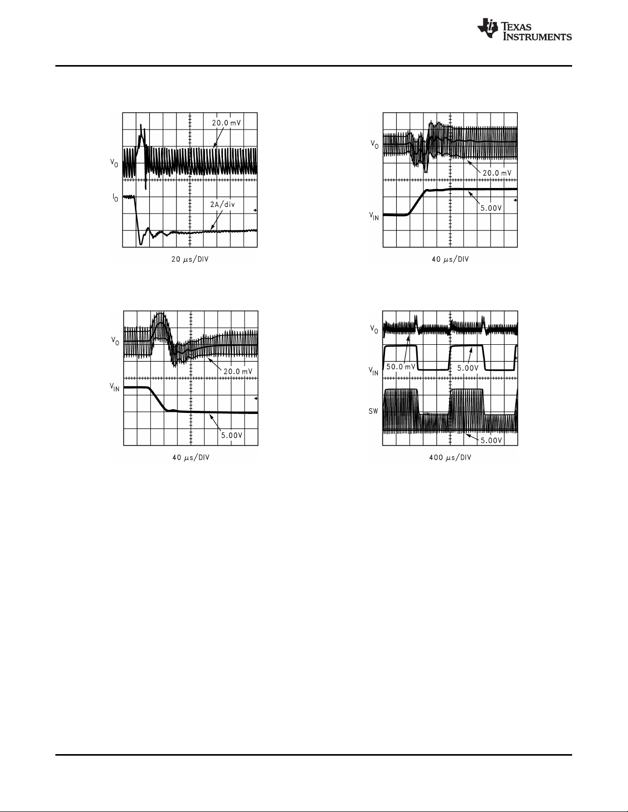
Typical Performance Characteristics (continued)
Load Transient Response (IO= 4 to 0A) Line Transient Response (VIN=5V to 12V)
Line Transient Response (VIN=12V to 5V) Line Transient Response
VIN= 12V, VO= 1.2V VO= 1.2V, IO= 5A
FSW= 300kHz FSW= 300kHz
Figure 20. Figure 21.
VO= 1.2V, IO= 5A VO= 1.2V, IO= 5A
FSW= 300kHz FSW= 300kHz
www.ti.com
Figure 22. Figure 23.
8 Submit Documentation Feedback Copyright © 2002–2013, Texas Instruments Incorporated
Product Folder Links: LM2727 LM2737
BG =
0.6V
50PA
10PA
OUTPUT CLAMP
HI: 3.25V
LO: 1.25V
3.25V
1.25V
SYNCHRONOUS
DRIVER LOGIC
10Ps
DELAY
0.708V
tol.=+/-2%
0.42V
tol.=+/-2%
hyst.=12%
SHUT
DOWN
LATCH
CLOCK &
RAMP
LOGIC
S
R
R>S
off
oc
UVLO
SD
FREQ
Vcc PGND SGND
FB
EAO
BOOT
HG
LG
ISEN
PWGD
SS
PGND
95P$
oc
off
off
20PA
EA
HIGH LOW
PWM
ILIM
3.05V
SS
CMP
LM2727, LM2737
www.ti.com
SNVS205D –AUGUST 2002–REVISED MARCH 2013
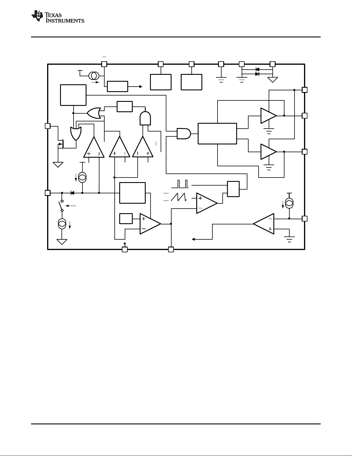
Block Diagram
Copyright © 2002–2013, Texas Instruments Incorporated Submit Documentation Feedback 9
Product Folder Links: LM2727 LM2737
LM2727, LM2737
SNVS205D –AUGUST 2002–REVISED MARCH 2013
www.ti.com
APPLICATION INFORMATION
THEORY OF OPERATION
The LM2727 is a voltage-mode, high-speed synchronous buck regulator with a PWM control scheme. It is
designed for use in set-top boxes, thin clients, DSL/Cable modems, and other applications that require high
efficiency buck converters. It has power good (PWRGD), output shutdown (SD), over voltage protection (OVP)
and under voltage protection (UVP). The over-voltage and under-voltage signals are OR gated to drive the
Power Good signal and a shutdown latch, which turns off the high side gate and turns on the low side gate if
pulled low. Current limit is achieved by sensing the voltage VDSacross the low side FET. During current limit the
high side gate is turned off and the low side gate turned on. The soft start capacitor is discharged by a 95µA
source (reducing the maximum duty cycle) until the current is under control. The LM2737 does not latch off
during UVP or OVP, and uses the HIGH and LOW comparators for the powergood function only.
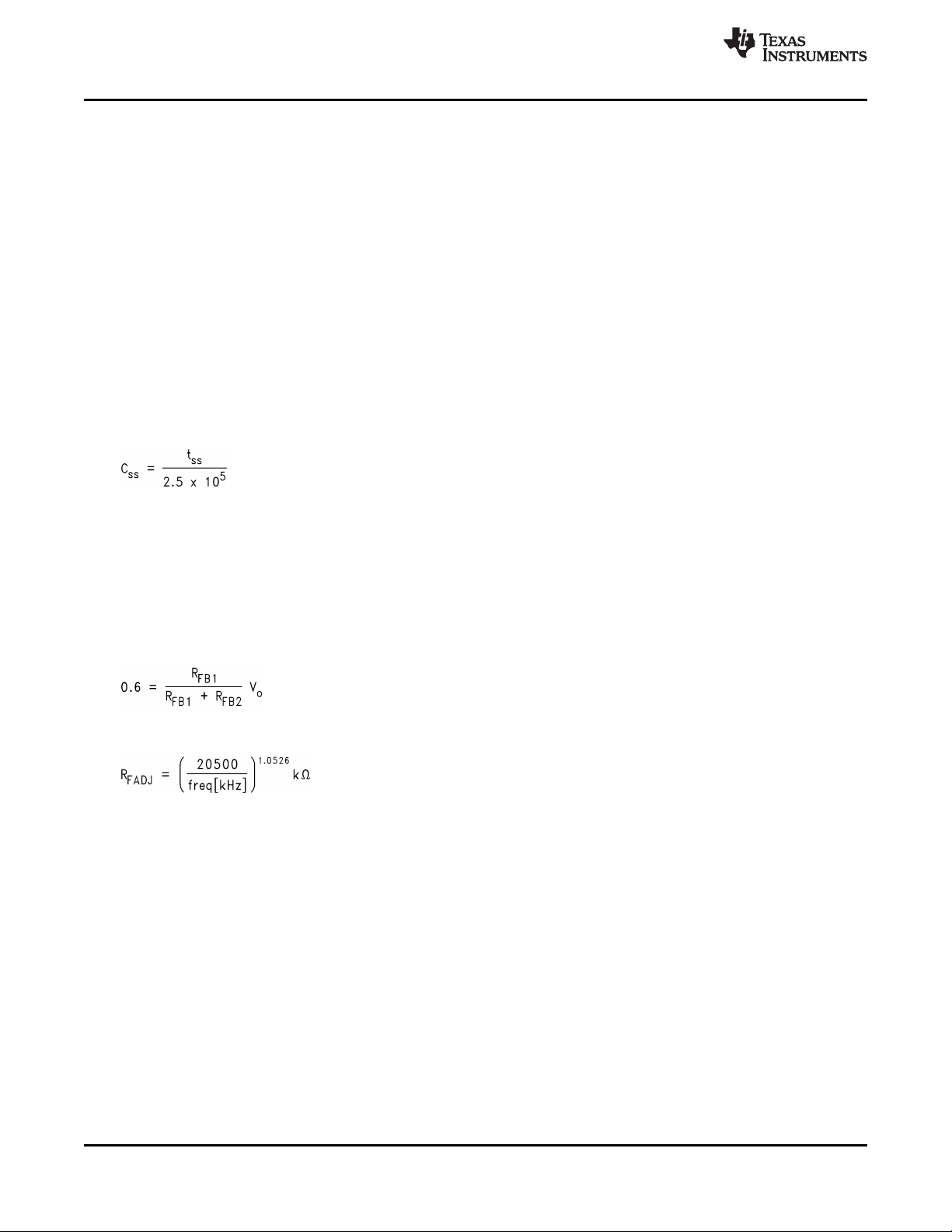
START UP
When VCCexceeds 4.2V and the enable pin EN sees a logic high the soft start capacitor begins charging through
an internal fixed 10µA source. During this time the output of the error amplifier is allowed to rise with the voltage
of the soft start capacitor. This capacitor, Css, determines soft start time, and can be determined approximately
by:
(1)
An application for a microprocessor might need a delay of 3ms, in which case CSSwould be 12nF. For a different
device, a 100ms delay might be more appropriate, in which case CSSwould be 400nF. (390 10%) During soft
start the PWRGD flag is forced low and is released when the voltage reaches a set value. At this point this chip
enters normal operation mode, the Power Good flag is released, and the OVP and UVP functions begin to
monitor Vo.
NORMAL OPERATION
While in normal operation mode, the LM2727/37 regulates the output voltage by controlling the duty cycle of the
high side and low side FETs. The equation governing output voltage is:
(2)
The PWM frequency is adjustable between 50kHz and 2MHz and is set by an external resistor, R
, between
FADJ
the FREQ pin and ground. The resistance needed for a desired frequency is approximately:
(3)
MOSFET GATE DRIVERS
The LM2727/37 has two gate drivers designed for driving N-channel MOSFETs in a synchronous mode. Power
for the drivers is supplied through the BOOTV pin. For the high side gate (HG) to fully turn on the top FET, the
BOOTV voltage must be at least one V
a separate, higher voltage source, or supplied from a local charge pump structure. In a system such as a
desktop computer, both 5V and 12V are usually available. Hence if Vin was 5V, the 12V supply could be used for
BOOTV. 12V is more than 2*Vin, so the HG would operate correctly. For a BOOTV of 12V, the initial gate
charging current is 2A, and the initial gate discharging current is typically 6A.
greater than Vin. (BOOTV ≥ 2*Vin) This voltage can be supplied by
GS(th)
10 Submit Documentation Feedback Copyright © 2002–2013, Texas Instruments Incorporated
Product Folder Links: LM2727 LM2737

LM27x7
BOOTV
HG
LG
+
+
5V
Vo
Cb
LM2727, LM2737
www.ti.com
SNVS205D –AUGUST 2002–REVISED MARCH 2013
Figure 24. BOOTV Supplied by Charge Pump
In a system without a separate, higher voltage, a charge pump (bootstrap) can be built using a diode and small
capacitor, Figure 24. The capacitor serves to maintain enough voltage between the top FET gate and source to
control the device even when the top FET is on and its source has risen up to the input voltage level.
The LM2727/37 gate drives use a BiCMOS design. Unlike some other bipolar control ICs, the gate drivers have
rail-to-rail swing, ensuring no spurious turn-on due to capacitive coupling.
POWER GOOD SIGNAL
The power good signal is the or-gated flag representing over-voltage and under-voltage protection. If the output
voltage is 18% over it's nominal value, VFB= 0.7V, or falls 30% below that value, VFB= 0.41V, the power good
flag goes low. The converter then turns off the high side gate, and turns on the low side gate. Unlike the output
(LM2727 only) the power good flag is not latched off. It will return to a logic high whenever the feedback pin
voltage is between 70% and 118% of 0.6V.
UVLO
The 4.2V turn-on threshold on VCChas a built in hysteresis of 0.6V. Therefore, if VCCdrops below 3.6V, the chip
enters UVLO mode. UVLO consists of turning off the top FET, turning on the bottom FET, and remaining in that
condition until VCCrises above 4.2V. As with shutdown, the soft start capacitor is discharged through a FET,
ensuring that the next start-up will be smooth.
CURRENT LIMIT
Current limit is realized by sensing the voltage across the low side FET while it is on. The R
known value, hence the current through the FET can be determined as:
VDS= I * R
DSON
The current limit is determined by an external resistor, RCS, connected between the switch node and the ISEN
pin. A constant current of 50µA is forced through Rcs, causing a fixed voltage drop. This fixed voltage is
compared against VDSand if the latter is higher, the current limit of the chip has been reached. RCScan be found
by using the following:
RCS= R
For example, a conservative 15A current limit in a 10A design with a minimum R
DSON
(LOW) * I
/50µA (5)
LIM
of 10mΩ would require a
DSON
3.3kΩ resistor. Because current sensing is done across the low side FET, no minimum high side on-time is
necessary. In the current limit mode the LM2727/37 will turn the high side off and the keep low side on for as
long as necessary. The chip also discharges the soft start capacitor through a fixed 95µA source. In this way,
smooth ramping up of the output voltage as with a normal soft start is ensured. The output of the LM2727/37
internal error amplifier is limited by the voltage on the soft start capacitor. Hence, discharging the soft start
capacitor reduces the maximum duty cycle D of the controller. During severe current limit, this reduction in duty
cycle will reduce the output voltage, if the current limit conditions lasts for an extended time.
During the first few nanoseconds after the low side gate turns on, the low side FET body diode conducts. This
causes an additional 0.7V drop in VDS. The range of VDSis normally much lower. For example, if R
10mΩ and the current through the FET was 10A, VDSwould be 0.1V. The current limit would see 0.7V as a 70A
current and enter current limit immediately. Hence current limit is masked during the time it takes for the high
side switch to turn off and the low side switch to turn on.
Copyright © 2002–2013, Texas Instruments Incorporated Submit Documentation Feedback 11
Product Folder Links: LM2727 LM2737
of the FET is a
DSON
DSON
(4)
were
LM2727, LM2737
SNVS205D –AUGUST 2002–REVISED MARCH 2013
www.ti.com
UVP/OVP
The output undervoltage protection and overvoltage protection mechanisms engage at 70% and 118% of the
target output voltage, respectively. In either case, the LM2727 will turn off the high side switch and turn on the
low side switch, and discharge the soft start capacitor through a MOSFET switch. The chip remains in this state
until the shutdown pin has been pulled to a logic low and then released. The UVP function is masked only during
the first charging of the soft start capacitor, when voltage is first applied to the VCCpin. In contrast, the LM2737 is
designed to continue operating during UVP or OVP conditions, and to resume normal operation once the fault
condition is cleared. As with the LM2727, the powergood flag goes low during this time, giving a logic-level
warning signal.
SHUT DOWN
If the shutdown pin SD is pulled low, the LM2727/37 discharges the soft start capacitor through a MOSFET
switch. The high side switch is turned off and the low side switch is turned on. The LM2727/37 remains in this
state until SD is released.
DESIGN CONSIDERATIONS
The following is a design procedure for all the components needed to create the circuit shown in Figure 26 in the
Example Circuits section, a 5V in to 1.2V out converter, capable of delivering 10A with an efficiency of 85%. The
switching frequency is 300kHz. The same procedures can be followed to create the circuit shown in Figure 26,
Figure 27, and to create many other designs with varying input voltages, output voltages, and output currents.
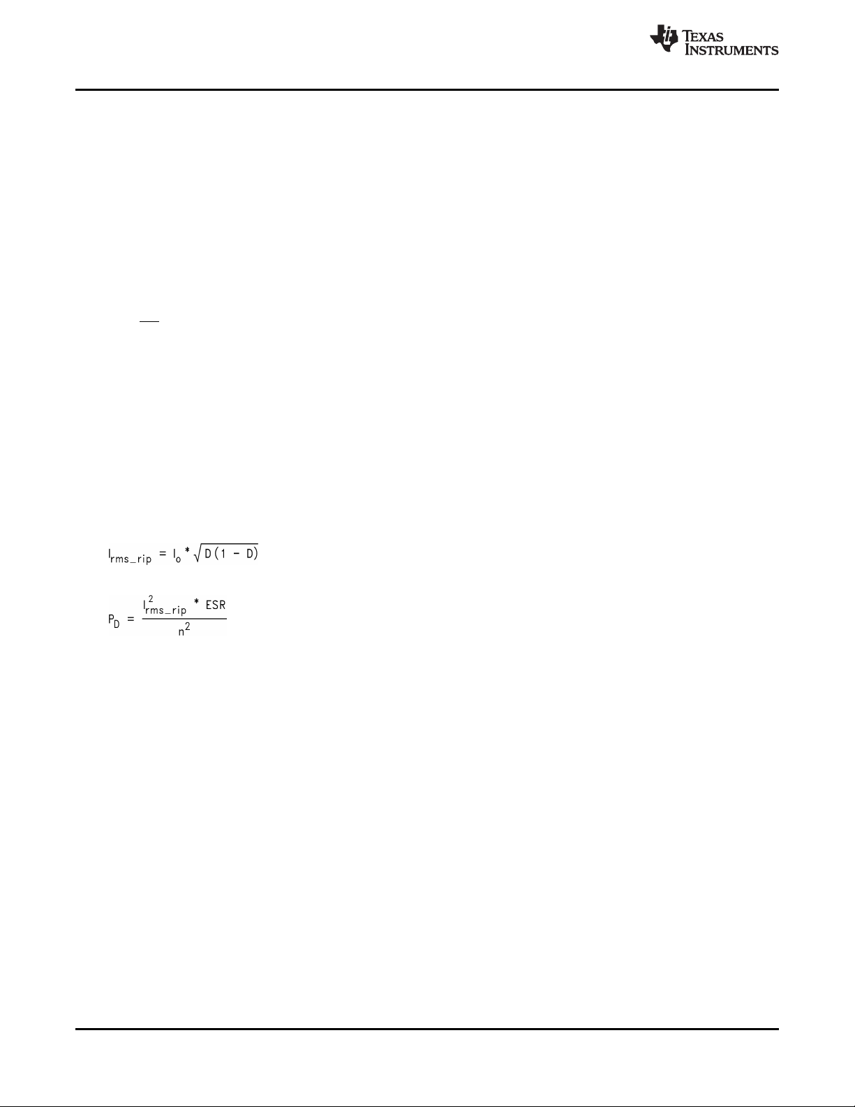
INPUT CAPACITOR
The input capacitors in a Buck switching converter are subjected to high stress due to the input current
waveform, which is a square wave. Hence input caps are selected for their ripple current capability and their
ability to withstand the heat generated as that ripple current runs through their ESR. Input rms ripple current is
approximately:
(6)
The power dissipated by each input capacitor is:
(7)
Here, n is the number of capacitors, and indicates that power loss in each cap decreases rapidly as the number
of input caps increase. The worst-case ripple for a Buck converter occurs during full load, when the duty cycle D
= 50%.
In the 5V to 1.2V case, D = 1.2/5 = 0.24. With a 10A maximum load the ripple current is 4.3A. The Sanyo
10MV5600AX aluminum electrolytic capacitor has a ripple current rating of 2.35A, up to 105°C. Two such
capacitors make a conservative design that allows for unequal current sharing between individual caps. Each
capacitor has a maximum ESR of 18mΩ at 100 kHz. Power loss in each device is then 0.05W, and total loss is
0.1W. Other possibilities for input and output capacitors include MLCC, tantalum, OSCON, SP, and POSCAPS.
INPUT INDUCTOR
The input inductor serves two basic purposes. First, in high power applications, the input inductor helps insulate
the input power supply from switching noise. This is especially important if other switching converters draw
current from the same supply. Noise at high frequency, such as that developed by the LM2727 at 1MHz
operation, could pass through the input stage of a slower converter, contaminating and possibly interfering with
its operation.
An input inductor also helps shield the LM2727 from high frequency noise generated by other switching
converters. The second purpose of the input inductor is to limit the input current slew rate. During a change from
no-load to full-load, the input inductor sees the highest voltage change across it, equal to the full load current
times the input capacitor ESR. This value divided by the maximum allowable input current slew rate gives the
minimum input inductance:
12 Submit Documentation Feedback Copyright © 2002–2013, Texas Instruments Incorporated
Product Folder Links: LM2727 LM2737
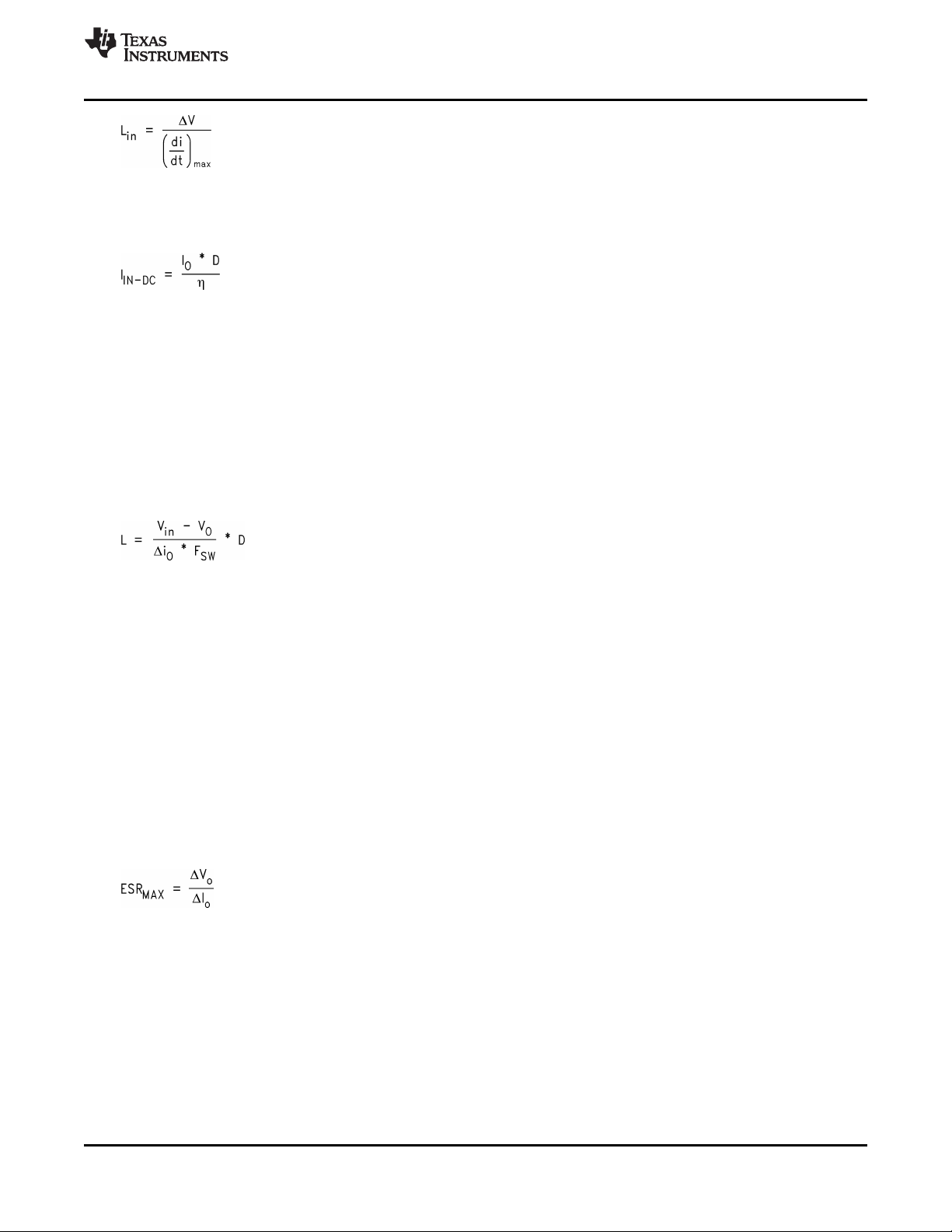
LM2727, LM2737
www.ti.com
SNVS205D –AUGUST 2002–REVISED MARCH 2013
(8)
In the case of a desktop computer system, the input current slew rate is the system power supply or "silver box"
output current slew rate, which is typically about 0.1A/µs. Total input capacitor ESR is 9mΩ, hence ΔV is
10*0.009 = 90 mV, and the minimum inductance required is 0.9µH. The input inductor should be rated to handle
the DC input current, which is approximated by:
(9)
In this case I
is about 2.8A. One possible choice is the TDK SLF12575T-1R2N8R2, a 1.2µH device that can
IN-DC
handle 8.2Arms, and has a DCR of 7mΩ.
OUTPUT INDUCTOR
The output inductor forms the first half of the power stage in a Buck converter. It is responsible for smoothing the
square wave created by the switching action and for controlling the output current ripple. (ΔIo) The inductance is
chosen by selecting between tradeoffs in efficiency and response time. The smaller the output inductor, the more
quickly the converter can respond to transients in the load current. As shown in the efficiency calculations,
however, a smaller inductor requires a higher switching frequency to maintain the same level of output current
ripple. An increase in frequency can mean increasing loss in the FETs due to the charging and discharging of the
gates. Generally the switching frequency is chosen so that conduction loss outweighs switching loss. The
equation for output inductor selection is:
(10)
Plugging in the values for output current ripple, input voltage, output voltage, switching frequency, and assuming
a 40% peak-to-peak output current ripple yields an inductance of 1.5µH. The output inductor must be rated to
handle the peak current (also equal to the peak switch current), which is (Io + 0.5*ΔIo). This is 12A for a 10A
design. The Coilcraft D05022-152HC is 1.5µH, is rated to 15Arms, and has a DCR of 4mΩ.
OUTPUT CAPACITOR
The output capacitor forms the second half of the power stage of a Buck switching converter. It is used to control
the output voltage ripple (ΔVo) and to supply load current during fast load transients.
In this example the output current is 10A and the expected type of capacitor is an aluminum electrolytic, as with
the input capacitors. (Other possibilities include ceramic, tantalum, and solid electrolyte capacitors, however the
ceramic type often do not have the large capacitance needed to supply current for load transients, and tantalums
tend to be more expensive than aluminum electrolytic.) Aluminum capacitors tend to have very high capacitance
and fairly low ESR, meaning that the ESR zero, which affects system stability, will be much lower than the
switching frequency. The large capacitance means that at switching frequency, the ESR is dominant, hence the
type and number of output capacitors is selected on the basis of ESR. One simple formula to find the maximum
ESR based on the desired output voltage ripple, ΔVoand the designed output current ripple, ΔIo, is:
(11)
In this example, in order to maintain a 2% peak-to-peak output voltage ripple and a 40% peak-to-peak inductor
current ripple, the required maximum ESR is 6mΩ. Three Sanyo 10MV5600AX capacitors in parallel will give an
equivalent ESR of 6mΩ. The total bulk capacitance of 16.8mF is enough to supply even severe load transients.
Using the same capacitors for both input and output also keeps the bill of materials simple.
Copyright © 2002–2013, Texas Instruments Incorporated Submit Documentation Feedback 13
Product Folder Links: LM2727 LM2737

LM2727, LM2737
SNVS205D –AUGUST 2002–REVISED MARCH 2013
www.ti.com
MOSFETS
MOSFETS are a critical part of any switching controller and have a direct impact on the system efficiency. In this
case the target efficiency is 85% and this is the variable that will determine which devices are acceptable. Loss
from the capacitors, inductors, and the LM2727 itself are detailed in the Efficiency section, and come to about
0.54W. To meet the target efficiency, this leaves 1.45W for the FET conduction loss, gate charging loss, and
switching loss. Switching loss is particularly difficult to estimate because it depends on many factors. When the
load current is more than about 1 or 2 amps, conduction losses outweigh the switching and gate charging losses.
This allows FET selection based on the R
of the FET. Adding the FET switching and gate-charging losses to
DSON
the equation leaves 1.2W for conduction losses. The equation for conduction loss is:
= D(I
2
* R
o
DSON
*k) + (1-D)(I
P
Cnd
The factor k is a constant which is added to account for the increasing R
1.3. The Si4442DY has a typical R
2
* R
o
DSON
*k) (12)
DSON
DSON
of 4.1mΩ. When plugged into the equation for P
of a FET due to heating. Here, k =
the result is a loss of
CND
0.533W. If this design were for a 5V to 2.5V circuit, an equal number of FETs on the high and low sides would be
the best solution. With the duty cycle D = 0.24, it becomes apparent that the low side FET carries the load
current 76% of the time. Adding a second FET in parallel to the bottom FET could improve the efficiency by
lowering the effective R
. The lower the duty cycle, the more effective a second or even third FET can be. For
DSON
a minimal increase in gate charging loss (0.054W) the decrease in conduction loss is 0.15W. What was an 85%
design improves to 86% for the added cost of one SO-8 MOSFET.
CONTROL LOOP COMPONENTS
The circuit is this design example and the others shown in the Example Circuits section have been compensated
to improve their DC gain and bandwidth. The result of this compensation is better line and load transient
responses. For the LM2727, the top feedback divider resistor, Rfb2, is also a part of the compensation. For the
10A, 5V to 1.2V design, the values are:
Cc1 = 4.7pF 10%, Cc2 = 1nF 10%, Rc = 229kΩ 1%. These values give a phase margin of 63° and a bandwidth
of 29.3kHz.
SUPPORT CAPACITORS AND RESISTORS
The Cinx capacitors are high frequency bypass devices, designed to filter harmonics of the switching frequency
and input noise. Two 1µF ceramic capacitors with a sufficient voltage rating (10V for the Circuit of Figure 26) will
work well in almost any case.
Rbypass and Cbypass are standard filter components designed to ensure smooth DC voltage for the chip supply
and for the bootstrap structure, if it is used. Use 10Ω for the resistor and a 2.2µF ceramic for the cap. Cb is the
bootstrap capacitor, and should be 0.1µF. (In the case of a separate, higher supply to the BOOTV pin, this 0.1µF
cap can be used to bypass the supply.) Using a Schottky device for the bootstrap diode allows the minimum drop
for both high and low side drivers. The On Semiconductor BAT54 or MBR0520 work well.
Rp is a standard pull-up resistor for the open-drain power good signal, and should be 10kΩ. If this feature is not
necessary, it can be omitted.
RCSis the resistor used to set the current limit. Since the design calls for a peak current magnitude (Io + 0.5 *
ΔIo) of 12A, a safe setting would be 15A. (This is well below the saturation current of the output inductor, which is
25A.) Following the equation from the Current Limit section, use a 3.3kΩ resistor.
R
is used to set the switching frequency of the chip. Following the equation in the Theory of Operation
FADJ
section, the closest 1% tolerance resistor to obtain fSW= 300kHz is 88.7kΩ.
CSSdepends on the users requirements. Based on the equation for CSSin the Theory of Operation section, for a
3ms delay, a 12nF capacitor will suffice.
14 Submit Documentation Feedback Copyright © 2002–2013, Texas Instruments Incorporated
Product Folder Links: LM2727 LM2737

LM2727, LM2737
www.ti.com
SNVS205D –AUGUST 2002–REVISED MARCH 2013
EFFICIENCY CALCULATIONS
A reasonable estimation of the efficiency of a switching controller can be obtained by adding together the loss is
each current carrying element and using the equation:
(13)
The following shows an efficiency calculation to complement the Circuit of Figure 26. Output power for this circuit
is 1.2V x 10A = 12W.
Chip Operating Loss
Q-V
*V
CC
CC
PIQ= I
2mA x 5V = 0.01W
FET Gate Charging Loss
PGC= n * VCC* QGS* f
OSC
The value n is the total number of FETs used. The Si4442DY has a typical total gate charge, QGS, of 36nC and
an r
of 4.1mΩ. For a single FET on top and bottom: 2*5*36E-9*300,000 = 0.108W
ds-on
FET Switching Loss
PSW= 0.5 * Vin* IO* (tr+ tf)* f
OSC
The Si4442DY has a typical rise time trand fall time tfof 11 and 47ns, respectively. 0.5*5*10*58E-9*300,000 =
0.435W
FET Conduction Loss
PCn= 0.533W (17)
Input Capacitor Loss
(14)
(15)
(16)
4.282*0.018/2 = 0.084W
Input Inductor Loss
2
P
= I
Lin
* DCR
in
input-L
2.822*0.007 = 0.055W
Output Inductor Loss
2
P
= I
Lout
* DCR
o
output-L
102*0.004 = 0.4W
System Efficiency
(18)
(19)
(20)
(21)
(22)
(23)
Copyright © 2002–2013, Texas Instruments Incorporated Submit Documentation Feedback 15
Product Folder Links: LM2727 LM2737

LM27x7
HG
BOOT
ISEN
LG
PGND
FB
Vcc
SD
PWGD
FREQ
SS
SGND
EAO
PGND
+
+
Vin = 5V
Vo = 1.2V@10A
3 x 5600 uF
10V, 3.1A
18 m:
1.5 uH
15 A, 4 m:
Rfb2
Rfb1
Cc1
Cc2 Rc1
Rcs
Css
Rfadj
Rin
Cin
D1
Cboot
Q1
Q2
1.2 uH
8.2 A, 6.9 m:
0.1u
1.5k
10
2.2u
88.7k
12n
270p
4.7p
229k
4.99k
4.99k
Co1-3
Lin
L1
2 x 5600uF
10V, 2.35A
Cin1,2
2x1uF
10V
Cinx1, 2
LM27x7
HG
BOOT
ISEN
LG
PGND
FB
Vcc
SD
PWGD
FREQ
SS
SGND
EAO
PGND
+
+
+5V
Vin = 12V
Vo = 3.3V@10A
2 x 10 uF
25V, 3.3A
4 x 100 uF
10V, 55 m:
2.7 uH
14.4 A, 4.5 m:
Rfb2
Rfb1
Cc1
Cc2 Rc1
Rcs
Css
Rfadj
Rin
Cin
D1
Cboot
Q1
Q2
1uF
25V
1.2 uH
8.2 A, 6.9 m:
Rc2 Cc3
0.1u
1.8k
10
2.2u
88.7k
12n
270p
6.8p
143.3k
8.45k 470p
11k
49.9k
Cin1,2
Cinx
Co1-4
Lin
L1
LM2727, LM2737
SNVS205D –AUGUST 2002–REVISED MARCH 2013
www.ti.com
Example Circuits
Figure 25. 5V-16V to 3.3V, 10A, 300kHz
This circuit and the one featured on the front page have been designed to deliver high current and high efficiency
in a small package, both in area and in height The tallest component in this circuit is the inductor L1, which is
6mm tall. The compensation has been designed to tolerate input voltages from 5 to 16V.
Figure 26. 5V to 1.2V, 10A, 300kHz
This circuit design, detailed in the Design Considerations section, uses inexpensive aluminum capacitors and offthe-shelf inductors. It can deliver 10A at better than 85% efficiency. Large bulk capacitance on input and output
ensure stable operation.
16 Submit Documentation Feedback Copyright © 2002–2013, Texas Instruments Incorporated
Product Folder Links: LM2727 LM2737

HG
BOOT
ISEN
LG
PGND
FB
Vcc
SD
PWGD
FREQ
SS
SGND
EAO
PGND
+
+
+5V
Vin = 3.3V
Vo = 0.8V@5A
1 x 5600 uF
10V, 2.35A
2 x 4700 uF
16V, 2.8A
1 uH
11 A, 3.7 m:
Rfb2
Rfb1
Cc1
Cc2
Rc1
Rcs
Css
Rfadj
Rin
Cin
D1
Cboot
Q1
Q2
1uF
10V
1 uH
4.5 A, 7.5 m:
4.99k
3.3k
14.9k
147k
4.7p
680p
12n
49.9k
2.2u
10
0.1u
Co1,2
Cin1
Cinx
Lin
L1
LM27x7
HG
BOOT
ISEN
LG
PGND
FB
Vcc
SD
PWGD
FREQ
SS
SGND
EAO
PGND
+
+
Vin = 5V
Vo = 1.8V@3A
100 uF
10V, 1.9A
1 x 220 uF
4V, 55 m:
2.2 uH
6.1A, 12 m:
Rfb2
Rfb1
Cc1
Cc2 Rc1
Rcs
Css
Rfadj
Rin
Cin
Cc
Q1/Q2
+12V
4.99k
2.49k
2.7k
12n
43.2k
10
2.2u
0.1u
10p
560p 51.1k
Cin1
Co1
L1
LM27x7
LM2727, LM2737
www.ti.com
SNVS205D –AUGUST 2002–REVISED MARCH 2013
Figure 27. 5V to 1.8V, 3A, 600kHz
The example circuit of Figure 27 has been designed for minimum component count and overall solution size. A
switching frequency of 600kHz allows the use of small input/output capacitors and a small inductor. The
availability of separate 5V and 12V supplies (such as those available from desk-top computer supplies) and the
low current further reduce component count. Using the 12V supply to power the MOSFET drivers eliminates the
bootstrap diode, D1. At low currents, smaller FETs or dual FETs are often the most efficient solutions. Here, the
Si4826DY, an asymmetric dual FET in an SO-8 package, yields 92% efficiency at a load of 2A.
Figure 28. 3.3V to 0.8V, 5A, 500kHz
The circuit of Figure 28 demonstrates the LM2727 delivering a low output voltage at high efficiency (87%) A
separate 5V supply is required to run the chip, however the input voltage can be as low as 2.2
Product Folder Links: LM2727 LM2737
Copyright © 2002–2013, Texas Instruments Incorporated Submit Documentation Feedback 17

LM27x7
HG
BOOT
ISEN
LG
PGND
FB
Vcc
SD
PWGD
FREQ
SS
SGND
EAO
PGND
+
+
+5V
Vin = 5 to 15V
Vo = 1.8V@1A
1 x 15uF
25V, 3.3A
1 x 15uF
25V 3.1mohm
3.3uH
4.1A, 17.4 m:
Rfb2
Rfb1
Cc1
Cc2 Rc1
Rcs
Css
Rfadj
Rin
Cin
D1
Cboot
1uH
6.4A, 7.3 m:
Rc2
Cc3
LM27x7
HG
BOOT
ISEN
LG
PGND
FB
Vcc
SD
PWGD
FREQ
SS
SGND
EAO
PGND
+
+
+5V
Vin = 5 to 15V
Vo = 3.3V@1A
1 x 15uF
25V, 3.3A
1 x 15uF
25V 3.1 m:
4.7uH
3.4A, 26 m:
Rfb2
Rfb1
Cc1
Cc2 Rc1
Rcs
Rfadj
Rin
Cin
D1
Cboot
Q1/Q2
1uH
6.4 A, 7.3 m:
Rc2
Cc3
10
2.2u
0.1u
1.5k
10k
2.21k
0.1u
10
2.2u
17.4k
39n
22p
680p 10.7k
680p66.5
10k
4.99k
1.5k
17.4k
27p
1n
820p
12.1k
54.9
Co1
Cin1
Lin
L1
L1
Lin
Co1
Q1/Q2
LM2727, LM2737
SNVS205D –AUGUST 2002–REVISED MARCH 2013
www.ti.com
Figure 29. 1.8V and 3.3V, 1A, 1.4MHz, Simultaneous
The circuits in Figure 29 are intended for ADSL applications, where the high switching frequency keeps noise out
of the data transmission range. In this design, the 1.8 and 3.3V outputs come up simultaneously by using the
same softstart capacitor. Because two current sources now charge the same capacitor, the capacitance must be
doubled to achieve the same softstart time. (Here, 40nF is used to achieve a 5ms softstart time.) A common
softstart capacitor means that, should one circuit enter current limit, the other circuit will also enter current limit.
In addition, if both circuits are built with the LM2727, a UVP or OVP fault on one circuit will cause both circuits to
latch off. The additional compensation components Rc2 and Cc3 are needed for the low ESR, all ceramic output
capacitors, and the wide (3x) range of Vin.
18 Submit Documentation Feedback Copyright © 2002–2013, Texas Instruments Incorporated
Product Folder Links: LM2727 LM2737

LM27x7
HG
BOOT
ISEN
LG
PGND
FB
Vcc
SD
PWGD
FREQ
SS
SGND
EAO
PGND
+
+
Vin = 12V
Vo = 5V@1.8A
2 x 680uF
16V
26 m:
47uH 2.7A
53 m:
Rfb2
Rfb1
Cc1
Cc2 Rc1
Css
Rfadj
Cin
Cboot
Q1
Rc2 Cc3
10uF
16V
10uF
6.3V
+5V (low current source)
D1
D2
10k
1.37k
22n
56p
3.9n 61.9k
750
12n
267k
0.1u
2.2u
L1
Cinx
Cox
Co1,2
680uF
16V
1.54A
Cin1
LM27x7
HG
BOOT
ISEN
LG
PGND
FB
Vcc
SD
PWGD
FREQ
SS
SGND
EAO
PGND
+
+
+5V
Vin = 11 to 13V
Vo = 3.3V@3A
4.2uH, 5.5A
15 m:
Rfb1
Cc1
Cc2 Rc1
Rcs
Css
Rfadj
Cin
D1
Cboot
Q1/Q2
1uH, 6.4A
7.3 m:
Rc2
Cc3
2 x 680uF
16V 1.54A
LM78L05
Vin = 11 to 13V
To 2nd LM27x7
2.21k
0.1u
2k
2.2u
32.5k
12n
8.2p
1n
4.7n2.37k
52.3k
Lin
Co1,2
680uF
16V, 1.54A
Cin1
10uF
16V
Cinx
Rfb2
10k
10uF
25V
Cox
LM2727, LM2737
www.ti.com
SNVS205D –AUGUST 2002–REVISED MARCH 2013
Figure 30. 12V Unregulated to 3.3V, 3A, 750kHz
This circuit shows the LM27x7 paired with a cost effective solution to provide the 5V chip power supply, using no
extra components other than the LM78L05 regulator itself. The input voltage comes from a 'brick' power supply
which does not regulate the 12V line tightly. Additional, inexpensive 10uF ceramic capacitors (Cinx and Cox)
help isolate devices with sensitive databands, such as DSL and cable modems, from switching noise and
harmonics.
Figure 31. 12V to 5V, 1.8A, 100kHz
In situations where low cost is very important, the LM27x7 can also be used as an asynchronous controller, as
shown in the above circuit. Although a a schottky diode in place of the bottom FET will not be as efficient, it will
cost much less than the FET. The 5V at low current needed to run the LM27x7 could come from a zener diode or
inexpensive regulator, such as the one shown in Figure 30. Because the LM27x7 senses current in the low side
MOSFET, the current limit feature will not function in an asynchronous design. The ISEN pin should be left open
in this case.
Copyright © 2002–2013, Texas Instruments Incorporated Submit Documentation Feedback 19
Product Folder Links: LM2727 LM2737

LM2727, LM2737
SNVS205D –AUGUST 2002–REVISED MARCH 2013
Table 1. Bill of Materials for Typical Application Circuit
ID Part Number Type Size Parameters Qty. Vendor
U1 LM2727 TSSOP-14 TSSOP-14 1
Q1, Q2 Si4884DY N-MOSFET SO-8 30V, 4.1mΩ, 36nC 1 Vishay
L1 RLF7030T-1R5N6R1 Inductor 7.1x7.1x3.2mm 1.5µH, 6.1A 9.6mΩ 1 TDK
Cin1, Cin2 C2012X5R1J106M MLCC 0805 10µF 6.3V 2 TDK
Cinx C3216X7R1E105K Capacitor 1206 1µF, 25V 1 TDK
Co1, Co2 6MV2200WG AL-E 10mm D 20mm H 2200µF 6.3V125mΩ 2 Sanyo
Cboot VJ1206X104XXA Capacitor 1206 0.1µF, 25V 1 Vishay
Cin C3216X7R1E225K Capacitor 1206 0.1µF, 25V 1 TDK
Css VJ1206X123KXX Capacitor 1206 12nF, 25V 1 Vishay
Cc1 VJ1206A2R2KXX Capacitor 1206 2.2pF 10% 1 Vishay
Cc2 VJ1206A181KXX Capacitor 1206 180pF 10% 1 Vishay
Rin CRCW1206100J Resistor 1206 10Ω 5% 1 Vishay
Rfadj CRCW12066342F Resistor 1206 63.4kΩ 1% 1 Vishay
Rc1 CRCW12063923F Resistor 1206 392kΩ 1% 1 Vishay
Rfb1 CRCW12061002F Resistor 1206 10kΩ 1% 1 Vishay
Rfb2 CRCW12061002F Resistor 1206 10kΩ 1% 1 Vishay
Rcs CRCW1206222J Resistor 1206 2.2kΩ 5% 1 Vishay
Synchronous Texas
Controller Instruments
www.ti.com
Table 2. Bill of Materials for Circuit of Figure 25
(Identical to BOM for 1.5V except as noted below)
ID Part Number Type Size Parameters Qty. Vendor
L1 RLF12560T-2R7N110 Inductor 12.5x12.8x6mm 2.7µH, 14.4A 4.5mΩ 1 TDK
Co1, Co2,
Co3, Co4
Cc1 VJ1206A6R8KXX Capacitor 1206 6.8pF 10% 1 Vishay
Cc2 VJ1206A271KXX Capacitor 1206 270pF 10% 1 Vishay
Cc3 VJ1206A471KXX Capacitor 1206 470pF 10% 1 Vishay
Rc2 CRCW12068451F Resistor 1206 8.45kΩ 1% 1 Vishay
Rfb1 CRCW12061102F Resistor 1206 11kΩ 1% 1 Vishay
10TPB100M POSCAP 7.3x4.3x2.8mm 100µF 10V 1.9Arms 4 Sanyo
Table 3. Bill of Materials for Circuit of Figure 26
ID Part Number Type Size Parameters Qty. Vendor
U1 LM2727 TSSOP-14 1
Q1 Si4442DY N-MOSFET SO-8 30V, 4.1mΩ, @ 4.5V, 36nC 1 Vishay
Q2 Si4442DY N-MOSFET SO-8 30V, 4.1mΩ, @ 4.5V, 36nC 1 Vishay
D1 BAT-54 Schottky Diode SOT-23 30V 1 Vishay
Lin SLF12575T-1R2N8R2 Inductor 12.5x12.5x7.5mm 12µH, 8.2A, 6.9mΩ 1 Coilcraft
L1 D05022-152HC Inductor 22.35x16.26x8mm 1.5µH, 15A,4mΩ 1 Coilcraft
Cin1, Cin2 10MV5600AX 16mm D 25mm H 5600µF10V 2.35Arms 2 Sanyo
Cinx C3216X7R1E105K Capacitor 1206 1µF, 25V 1 TDK
Co1, Co2, Aluminum
Co3 Electrolytic
Cboot VJ1206X104XXA Capacitor 1206 0.1µF, 25V 1 Vishay
Cin C3216X7R1E225K Capacitor 1206 2.2µF, 25V 1 TDK
Css VJ1206X123KXX Capacitor 1206 12nF, 25V 1 Vishay
Cc1 VJ1206A4R7KXX Capacitor 1206 4.7pF 10% 1 Vishay
10MV5600AX 16mm D 25mm H 5600µF10V 2.35Arms 2 Sanyo
Synchronous Texas
Controller Instruments
Aluminum
Electrolytic
20 Submit Documentation Feedback Copyright © 2002–2013, Texas Instruments Incorporated
Product Folder Links: LM2727 LM2737

LM2727, LM2737
www.ti.com
SNVS205D –AUGUST 2002–REVISED MARCH 2013
Table 3. Bill of Materials for Circuit of Figure 26 (continued)
ID Part Number Type Size Parameters Qty. Vendor
Cc2 VJ1206A102KXX Capacitor 1206 1nF 10% 1 Vishay
Rin CRCW1206100J Resistor 1206 10Ω 5% 1 Vishay
Rfadj CRCW12068872F Resistor 1206 88.7kΩ 1% 1 Vishay
Rc1 CRCW12062293F Resistor 1206 229kΩ 1% 1 Vishay
Rfb1 CRCW12064991F Resistor 1206 4.99kΩ 1% 1 Vishay
Rfb2 CRCW12064991F Resistor 1206 4.99kΩ 1% 1 Vishay
Rcs CRCW1206152J Resistor 1206 1.5kΩ 5% 1 Vishay
Table 4. Bill of Materials for Circuit of Figure 27
ID Part Number Type Size Parameters Qty. Vendor
U1 LM2727 Synchronous TSSOP-14 1 Texas
Q1/Q2 Si4826DY Asymetric Dual SO-8 30V, 24mΩ/ 8nC 1 Vishay
L1 DO3316P-222 Inductor 12.95x9.4x 5.21mm 2.2µH, 6.1A, 12mΩ 1 Coilcraft
Cin1 10TPB100ML POSCAP 7.3x4.3x3.1mm 100µF 10V 1.9Arms 1 Sanyo
Co1 4TPB220ML POSCAP 7.3x4.3x3.1mm 220µF 4V 1.9Arms 1 Sanyo
Cc C3216X7R1E105K Capacitor 1206 1µF, 25V 1 TDK
Cin C3216X7R1E225K Capacitor 1206 2.2µF, 25V 1 TDK
Css VJ1206X123KXX Capacitor 1206 12nF, 25V 1 Vishay
Cc1 VJ1206A100KXX Capacitor 1206 10pF 10% 1 Vishay
Cc2 VJ1206A561KXX Capacitor 1206 560pF 10% 1 Vishay
Rin CRCW1206100J Resistor 1206 10Ω 5% 1 Vishay
Rfadj CRCW12064222F Resistor 1206 42.2kΩ 1% 1 Vishay
Rc1 CRCW12065112F Resistor 1206 51.1kΩ 1% 1 Vishay
Rfb1 CRCW12062491F Resistor 1206 2.49kΩ 1% 1 Vishay
Rfb2 CRCW12064991F Resistor 1206 4.99kΩ 1% 1 Vishay
Rcs CRCW1206272J Resistor 1206 2.7kΩ 5% 1 Vishay
Controller Instruments
N-MOSFET Top 16.5mΩ/ 15nC
Table 5. Bill of Materials for Circuit of Figure 28
ID Part Number Type Size Parameters Qty. Vendor
U1 LM2727 Synchronous TSSOP-14 1 Texas
Q1 Si4884DY N-MOSFET SO-8 30V, 13.5mΩ, @ 4.5V 1 Vishay
Q2 Si4884DY N-MOSFET SO-8 30V, 13.5mΩ, @ 4.5V 1 Vishay
D1 BAT-54 Schottky Diode SOT-23 30V 1 Vishay
Lin P1166.102T Inductor 7.29x7.29 3.51mm 1µH, 11A 3.7mΩ 1 Pulse
L1 P1168.102T Inductor 12x12x4.5 mm 1µH, 11A, 3.7mΩ 1 Pulse
Cin1 10MV5600AX Aluminum 16mm D 25mm H 5600µF 10V 2.35Arms 1 Sanyo
Cinx C3216X7R1E105K Capacitor 1206 1µF, 25V 1 TDK
Co1, Co2, 16MV4700WX Aluminum 12.5mm D 30mm H 4700µF 16V 2.8Arms 2 Sanyo
Co3 Electrolytic
Cboot VJ1206X104XXA Capacitor 1206 0.1µF, 25V 1 Vishay
Cin C3216X7R1E225K Capacitor 1206 2.2µF, 25V 1 TDK
Css VJ1206X123KXX Capacitor 1206 12nF, 25V 1 Vishay
Cc1 VJ1206A4R7KXX Capacitor 1206 4.7pF 10% 1 Vishay
Copyright © 2002–2013, Texas Instruments Incorporated Submit Documentation Feedback 21
Controller Instruments
15.3nC
15.3nC
Electrolytic
Product Folder Links: LM2727 LM2737

LM2727, LM2737
SNVS205D –AUGUST 2002–REVISED MARCH 2013
Table 5. Bill of Materials for Circuit of Figure 28 (continued)
ID Part Number Type Size Parameters Qty. Vendor
Cc2 VJ1206A681KXX Capacitor 1206 680pF 10% 1 Vishay
Rin CRCW1206100J Resistor 1206 10Ω 5% 1 Vishay
Rfadj CRCW12064992F Resistor 1206 49.9kΩ 1% 1 Vishay
Rc1 CRCW12061473F Resistor 1206 147kΩ 1% 1 Vishay
Rfb1 CRCW12061492F Resistor 1206 14.9kΩ 1% 1 Vishay
Rfb2 CRCW12064991F Resistor 1206 4.99kΩ 1% 1 Vishay
Rcs CRCW1206332J Resistor 1206 3.3kΩ 5% 1 Vishay
Table 6. Bill of Materials for Circuit of Figure 29
ID Part Number Type Size Parameters Qty. Vendor
U1 LM2727 Synchronous TSSOP-14 1 Texas
Controller Instruments
Q1/Q2 Si4826DY Assymetric Dual SO-8 30V, 24mΩ/ 8nC 1 Vishay
N-MOSFET Top 16.5mΩ/ 15nC
D1 BAT-54 Schottky Diode SOT-23 30V 1 Vishay
Lin RLF7030T-1R0N64 Inductor 6.8x7.1x3.2mm 1µH, 6.4A, 7.3mΩ 1 TDK
L1 RLF7030T-3R3M4R1 Inductor 6.8x7.1x3.2mm 3.3µH, 4.1A, 17.4mΩ 1 TDK
Cin1 C4532X5R1E156M MLCC 1812 15µF 25V 3.3Arms 1 Sanyo
Co1 C4532X5R1E156M MLCC 1812 15µF 25V 3.3Arms 1 Sanyo
Cboot VJ1206X104XXA Capacitor 1206 0.1µF, 25V 1 TDK
Cin C3216X7R1E225K Capacitor 1206 2.2µF, 25V 1 TDK
Css VJ1206X393KXX Capacitor 1206 39nF, 25V 1 Vishay
Cc1 VJ1206A220KXX Capacitor 1206 22pF 10% 1 Vishay
Cc2 VJ1206A681KXX Capacitor 1206 680pF 10% 1 Vishay
Cc3 VJ1206A681KXX Capacitor 1206 680pF 10% 1 Vishay
Rin CRCW1206100J Resistor 1206 10Ω 5% 1 Vishay
Rfadj CRCW12061742F Resistor 1206 17.4kΩ 1% 1 Vishay
Rc1 CRCW12061072F Resistor 1206 10.7kΩ 1% 1 Vishay
Rc2 CRCW120666R5F Resistor 1206 66.5Ω 1% 1 Vishay
Rfb1 CRCW12064991F Resistor 1206 4.99kΩ 1% 1 Vishay
Rfb2 CRCW12061002F Resistor 1206 10kΩ 1% 1 Vishay
Rcs CRCW1206152J Resistor 1206 1.5kΩ 5% 1 Vishay
www.ti.com
Table 7. Bill of Materials for 3.3V Circuit of Figure 29
(Identical to BOM for 1.8V except as noted below)
ID Part Number Type Size Parameters Qty. Vendor
L1 RLF7030T-4R7M3R4 Inductor 6.8x7.1x 3.2mm 4.7µH, 3.4A, 26mΩ 1 TDK
Cc1 VJ1206A270KXX Capacitor 1206 27pF 10% 1 Vishay
Cc2 VJ1206X102KXX Capacitor 1206 1nF 10% 1 Vishay
Cc3 VJ1206A821KXX Capacitor 1206 820pF 10% 1 Vishay
Rc1 CRCW12061212F Resistor 1206 12.1kΩ 1% 1 Vishay
Rc2 CRCW12054R9F Resistor 1206 54.9Ω 1% 1 Vishay
Rfb1 CRCW12062211F Resistor 1206 2.21kΩ 1% 1 Vishay
Rfb2 CRCW12061002F Resistor 1206 10kΩ 1% 1 Vishay
22 Submit Documentation Feedback Copyright © 2002–2013, Texas Instruments Incorporated
Product Folder Links: LM2727 LM2737

LM2727, LM2737
www.ti.com
SNVS205D –AUGUST 2002–REVISED MARCH 2013
Table 8. Bill of Materials for Circuit of Figure 30
ID Part Number Type Size Parameters Qty. Vendor
U1 LM2727 Synchronous Controller TSSOP-14 1 Texas
U2 LM78L05 Voltage Regulator SO-8 1 Texas
Q1/Q2 Si4826DY Assymetric Dual N-MOSFET SO-8 30V, 24mΩ/ 8nC 1 Vishay
Top 16.5mΩ/ 15nC
D1 BAT-54 Schottky Diode SOT-23 30V 1 Vishay
Lin RLF7030T-1R0N64 Inductor 6.8x7.1x3.2mm 1µH, 6.4A, 7.3mΩ 1 TDK
L1 SLF12565T-4R2N5R5 Inductor 12.5x12.5x6.5mm 4.2µH, 5.5A, 15mΩ 1 TDK
Cin1 16MV680WG Al-E D: 10mm L: 12.5mm 680µF 16V 3.4Arms 1 Sanyo
Cinx C3216X5R1C106M MLCC 1210 10µF 16V 3.4Arms 1 TDK
Co1 Co2 16MV680WG MLCC 1812 15µF 25V 3.3Arms 1 Sanyo
Cox C3216X5R10J06M MLCC 1206 10µF 6.3V 2.7A TDK
Cboot VJ1206X104XXA Capacitor 1206 0.1µF, 25V 1 Vishay
Cin C3216X7R1E225K Capacitor 1206 2.2µF, 25V 1 TDK
Css VJ1206X123KXX Capacitor 1206 12nF, 25V 1 Vishay
Cc1 VJ1206A8R2KXX Capacitor 1206 8.2pF 10% 1 Vishay
Cc2 VJ1206X102KXX Capacitor 1206 1nF 10% 1 Vishay
Cc3 VJ1206X472KXX Capacitor 1206 4.7nF 10% 1 Vishay
Rfadj CRCW12063252F Resistor 1206 32.5kΩ 1% 1 Vishay
Rc1 CRCW12065232F Resistor 1206 52.3kΩ 1% 1 Vishay
Rc2 CRCW120662371F Resistor 1206 2.37Ω 1% 1 Vishay
Rfb1 CRCW12062211F Resistor 1206 2.21kΩ 1% 1 Vishay
Rfb2 CRCW12061002F Resistor 1206 10kΩ 1% 1 Vishay
Rcs CRCW1206202J Resistor 1206 2kΩ 5% 1 Vishay
Instrument
Instrument
s
s
Table 9. Bill of Materials for Circuit of Figure 31
ID Part Number Type Size Parameters Qty. Vendor
U1 LM2727 Synchronous TSSOP-14 1 Texas
Q1 Si4894DY N-MOSFET SO-8 30V, 15mΩ, 11.5nC 1 Vishay
D2 MBRS330T3 Schottky Diode SO-8 30V, 3A 1 ON
L1 SLF12565T-470M2R4 Inductor 12.5x12.8x 4.7mm 47µH, 2.7A 53mΩ 1 TDK
D1 MBR0520 Schottky Diode 1812 20V 0.5A 1 ON
Cin1 16MV680WG Al-E 1206 680µF, 16V, 1.54Arms 1 Sanyo
Cinx C3216X5R1C106M MLCC 1206 10µF, 16V, 3.4Arms 1 TDK
Co1, Co2 16MV680WG Al-E D: 10mm L: 12.5mm 680µF 16V 26mΩ 2 Sanyo
Cox C3216X5R10J06M MLCC 1206 10µF, 6.3V 2.7A 1 TDK
Cboot VJ1206X104XXA Capacitor 1206 0.1µF, 25V 1 Vishay
Cin C3216X7R1E225K Capacitor 1206 2.2µF, 25V 1 TDK
Css VJ1206X123KXX Capacitor 1206 12nF, 25V 1 Vishay
Cc1 VJ1206A561KXX Capacitor 1206 56pF 10% 1 Vishay
Cc2 VJ1206X392KXX Capacitor 1206 3.9nF 10% 1 Vishay
Cc3 VJ1206X223KXX Capacitor 1206 22nF 10% 1 Vishay
Rfadj CRCW12062673F Resistor 1206 267kΩ 1% 1 Vishay
Rc1 CRCW12066192F Resistor 1206 61.9kΩ 1% 1 Vishay
Rc2 CRCW12067503F Resistor 1206 750kΩ 1% 1 Vishay
Copyright © 2002–2013, Texas Instruments Incorporated Submit Documentation Feedback 23
Controller Instruments
Product Folder Links: LM2727 LM2737

LM2727, LM2737
SNVS205D –AUGUST 2002–REVISED MARCH 2013
Table 9. Bill of Materials for Circuit of Figure 31 (continued)
ID Part Number Type Size Parameters Qty. Vendor
Rfb1 CRCW12061371F Resistor 1206 1.37kΩ 1% 1 Vishay
Rfb2 CRCW12061002F Resistor 1206 10kΩ 1% 1 Vishay
Rcs CRCW1206122F Resistor 1206 1.2kΩ 5% 1 Vishay
www.ti.com
24 Submit Documentation Feedback Copyright © 2002–2013, Texas Instruments Incorporated
Product Folder Links: LM2727 LM2737

LM2727, LM2737
www.ti.com
SNVS205D –AUGUST 2002–REVISED MARCH 2013
REVISION HISTORY
Changes from Revision C (March 2013) to Revision D Page
• Changed layout of National Data Sheet to TI format .......................................................................................................... 23
Copyright © 2002–2013, Texas Instruments Incorporated Submit Documentation Feedback 25
Product Folder Links: LM2727 LM2737
PACKAGE OPTION ADDENDUM
www.ti.com
PACKAGING INFORMATION
Orderable Device Status
LM2727MTC NRND TSSOP PW 14 94 TBD Call TI Call TI 0 to 125 2727
LM2727MTC/NOPB ACTIVE TSSOP PW 14 94 Green (RoHS
LM2727MTCX/NOPB ACTIVE TSSOP PW 14 2500 Green (RoHS
LM2737MTC NRND TSSOP PW 14 94 TBD Call TI Call TI -40 to 125 2737
LM2737MTC/NOPB ACTIVE TSSOP PW 14 94 Green (RoHS
LM2737MTCX NRND TSSOP PW 14 2500 TBD Call TI Call TI -40 to 125 2737
LM2737MTCX/NOPB ACTIVE TSSOP PW 14 2500 Green (RoHS
(1)
The marketing status values are defined as follows:
ACTIVE: Product device recommended for new designs.
LIFEBUY: TI has announced that the device will be discontinued, and a lifetime-buy period is in effect.
NRND: Not recommended for new designs. Device is in production to support existing customers, but TI does not recommend using this part in a new design.
PREVIEW: Device has been announced but is not in production. Samples may or may not be available.
OBSOLETE: TI has discontinued the production of the device.
Package Type Package
(1)
Drawing
Pins Package
Qty
Eco Plan
(2)
& no Sb/Br)
& no Sb/Br)
& no Sb/Br)
& no Sb/Br)
Lead/Ball Finish
(6)
CU NIPDAU | CU SN Level-1-260C-UNLIM 0 to 125 2727
CU NIPDAU | CU SN Level-1-260C-UNLIM 0 to 125 2727
CU NIPDAU | CU SN Level-1-260C-UNLIM -40 to 125 2737
CU NIPDAU | CU SN Level-1-260C-UNLIM -40 to 125 2737
MSL Peak Temp
(3)
Op Temp (°C) Device Marking
MTC
MTC
MTC
MTC
MTC
MTC
MTC
(4/5)
(2)
Eco Plan - The planned eco-friendly classification: Pb-Free (RoHS), Pb-Free (RoHS Exempt), or Green (RoHS & no Sb/Br) - please check http://www.ti.com/productcontent for the latest availability
information and additional product content details.
TBD: The Pb-Free/Green conversion plan has not been defined.
Pb-Free (RoHS): TI's terms "Lead-Free" or "Pb-Free" mean semiconductor products that are compatible with the current RoHS requirements for all 6 substances, including the requirement that
lead not exceed 0.1% by weight in homogeneous materials. Where designed to be soldered at high temperatures, TI Pb-Free products are suitable for use in specified lead-free processes.
Pb-Free (RoHS Exempt): This component has a RoHS exemption for either 1) lead-based flip-chip solder bumps used between the die and package, or 2) lead-based die adhesive used between
the die and leadframe. The component is otherwise considered Pb-Free (RoHS compatible) as defined above.
Green (RoHS & no Sb/Br): TI defines "Green" to mean Pb-Free (RoHS compatible), and free of Bromine (Br) and Antimony (Sb) based flame retardants (Br or Sb do not exceed 0.1% by weight
in homogeneous material)
(3)
MSL, Peak Temp. - The Moisture Sensitivity Level rating according to the JEDEC industry standard classifications, and peak solder temperature.
(4)
There may be additional marking, which relates to the logo, the lot trace code information, or the environmental category on the device.
5-Sep-2014
Samples
Addendum-Page 1

PACKAGE OPTION ADDENDUM
www.ti.com
(5)
Multiple Device Markings will be inside parentheses. Only one Device Marking contained in parentheses and separated by a "~" will appear on a device. If a line is indented then it is a continuation
of the previous line and the two combined represent the entire Device Marking for that device.
(6)
Lead/Ball Finish - Orderable Devices may have multiple material finish options. Finish options are separated by a vertical ruled line. Lead/Ball Finish values may wrap to two lines if the finish
value exceeds the maximum column width.
Important Information and Disclaimer:The information provided on this page represents TI's knowledge and belief as of the date that it is provided. TI bases its knowledge and belief on information
provided by third parties, and makes no representation or warranty as to the accuracy of such information. Efforts are underway to better integrate information from third parties. TI has taken and
continues to take reasonable steps to provide representative and accurate information but may not have conducted destructive testing or chemical analysis on incoming materials and chemicals.
TI and TI suppliers consider certain information to be proprietary, and thus CAS numbers and other limited information may not be available for release.
In no event shall TI's liability arising out of such information exceed the total purchase price of the TI part(s) at issue in this document sold by TI to Customer on an annual basis.
5-Sep-2014
Addendum-Page 2

PACKAGE MATERIALS INFORMATION
www.ti.com 30-Apr-2016
TAPE AND REEL INFORMATION
*All dimensions are nominal
Device Package
Type
LM2727MTCX/NOPB TSSOP PW 14 2500 330.0 12.4 6.95 5.6 1.6 8.0 12.0 Q1
LM2737MTCX TSSOP PW 14 2500 330.0 12.4 6.95 5.6 1.6 8.0 12.0 Q1
LM2737MTCX/NOPB TSSOP PW 14 2500 330.0 12.4 6.95 5.6 1.6 8.0 12.0 Q1
Package
Drawing
Pins SPQ Reel
Diameter
(mm)
Reel
Width
W1 (mm)
A0
(mm)B0(mm)K0(mm)P1(mm)W(mm)
Pin1
Quadrant
Pack Materials-Page 1

PACKAGE MATERIALS INFORMATION
www.ti.com 30-Apr-2016
*All dimensions are nominal
Device Package Type Package Drawing Pins SPQ Length (mm) Width (mm) Height (mm)
LM2727MTCX/NOPB TSSOP PW 14 2500 367.0 367.0 35.0
LM2737MTCX TSSOP PW 14 2500 367.0 367.0 35.0
LM2737MTCX/NOPB TSSOP PW 14 2500 367.0 367.0 35.0
Pack Materials-Page 2


IMPORTANT NOTICE
Texas Instruments Incorporated and its subsidiaries (TI) reserve the right to make corrections, enhancements, improvements and other
changes to its semiconductor products and services per JESD46, latest issue, and to discontinue any product or service per JESD48, latest
issue. Buyers should obtain the latest relevant information before placing orders and should verify that such information is current and
complete. All semiconductor products (also referred to herein as “components”) are sold subject to TI’s terms and conditions of sale
supplied at the time of order acknowledgment.
TI warrants performance of its components to the specifications applicable at the time of sale, in accordance with the warranty in TI’s terms
and conditions of sale of semiconductor products. Testing and other quality control techniques are used to the extent TI deems necessary
to support this warranty. Except where mandated by applicable law, testing of all parameters of each component is not necessarily
performed.
TI assumes no liability for applications assistance or the design of Buyers’ products. Buyers are responsible for their products and
applications using TI components. To minimize the risks associated with Buyers’ products and applications, Buyers should provide
adequate design and operating safeguards.
TI does not warrant or represent that any license, either express or implied, is granted under any patent right, copyright, mask work right, or
other intellectual property right relating to any combination, machine, or process in which TI components or services are used. Information
published by TI regarding third-party products or services does not constitute a license to use such products or services or a warranty or
endorsement thereof. Use of such information may require a license from a third party under the patents or other intellectual property of the
third party, or a license from TI under the patents or other intellectual property of TI.
Reproduction of significant portions of TI information in TI data books or data sheets is permissible only if reproduction is without alteration
and is accompanied by all associated warranties, conditions, limitations, and notices. TI is not responsible or liable for such altered
documentation. Information of third parties may be subject to additional restrictions.
Resale of TI components or services with statements different from or beyond the parameters stated by TI for that component or service
voids all express and any implied warranties for the associated TI component or service and is an unfair and deceptive business practice.
TI is not responsible or liable for any such statements.
Buyer acknowledges and agrees that it is solely responsible for compliance with all legal, regulatory and safety-related requirements
concerning its products, and any use of TI components in its applications, notwithstanding any applications-related information or support
that may be provided by TI. Buyer represents and agrees that it has all the necessary expertise to create and implement safeguards which
anticipate dangerous consequences of failures, monitor failures and their consequences, lessen the likelihood of failures that might cause
harm and take appropriate remedial actions. Buyer will fully indemnify TI and its representatives against any damages arising out of the use
of any TI components in safety-critical applications.
In some cases, TI components may be promoted specifically to facilitate safety-related applications. With such components, TI’s goal is to
help enable customers to design and create their own end-product solutions that meet applicable functional safety standards and
requirements. Nonetheless, such components are subject to these terms.
No TI components are authorized for use in FDA Class III (or similar life-critical medical equipment) unless authorized officers of the parties
have executed a special agreement specifically governing such use.
Only those TI components which TI has specifically designated as military grade or “enhanced plastic” are designed and intended for use in
military/aerospace applications or environments. Buyer acknowledges and agrees that any military or aerospace use of TI components
which have not been so designated is solely at the Buyer's risk, and that Buyer is solely responsible for compliance with all legal and
regulatory requirements in connection with such use.
TI has specifically designated certain components as meeting ISO/TS16949 requirements, mainly for automotive use. In any case of use of
non-designated products, TI will not be responsible for any failure to meet ISO/TS16949.
Products Applications
Audio www.ti.com/audio Automotive and Transportation www.ti.com/automotive
Amplifiers amplifier.ti.com Communications and Telecom www.ti.com/communications
Data Converters dataconverter.ti.com Computers and Peripherals www.ti.com/computers
DLP® Products www.dlp.com Consumer Electronics www.ti.com/consumer-apps
DSP dsp.ti.com Energy and Lighting www.ti.com/energy
Clocks and Timers www.ti.com/clocks Industrial www.ti.com/industrial
Interface interface.ti.com Medical www.ti.com/medical
Logic logic.ti.com Security www.ti.com/security
Power Mgmt power.ti.com Space, Avionics and Defense www.ti.com/space-avionics-defense
Microcontrollers microcontroller.ti.com Video and Imaging www.ti.com/video
RFID www.ti-rfid.com
OMAP Applications Processors www.ti.com/omap TI E2E Community e2e.ti.com
Wireless Connectivity www.ti.com/wirelessconnectivity
Mailing Address: Texas Instruments, Post Office Box 655303, Dallas, Texas 75265
Copyright © 2016, Texas Instruments Incorporated

 Loading...