

Texas Instruments LM393PWLE, LM393PSR, LM393PSLE, LM393P, LM393APWR Datasheet
...
LM193, LM293, LM293A, LM393
LM393A, LM393Y, LM2903, LM2903Q
DUAL DIFFERENTIAL COMPARATORS
SLCS005E – JUNE 1976 – REVISED NOVEMBER 1999
1
POST OFFICE BOX 655303 • DALLAS, TEXAS 75265
D
Single Supply or Dual Supplies
D
Wide Range of Supply Voltage
...2 V to 36 V
D
Low Supply-Current Drain Independent of
Supply Voltage . . . 0.4 mA Typ Per
Comparator
D
Low Input Bias Current . . . 25 nA Typ
D
Low Input Offset Current ...3 nA Typ
(LM193)
D
Low Input Offset Voltage ...2 mV Typ
D
Common-Mode Input Voltage Range
Includes Ground
D
Differential Input Voltage Range Equal to
Maximum-Rated Supply V oltage . . . ±36 V
D
Low Output Saturation Voltage
D
Output Compatible With TTL, MOS, and
CMOS
description
These devices consist of two independent voltage
comparators that are designed to operate from a
single power supply over a wide range of voltages.
Operation from dual supplies also is possible as
long as the difference between the two supplies is 2 V to 36 V , and V
CC
is at least 1.5 V more positive than the
input common-mode voltage. Current drain is independent of the supply voltage. The outputs can be connected
to other open-collector outputs to achieve wired-AND relationships.
The LM193 is characterized for operation from –55°C to 125°C. The LM293 and LM293A are characterized for
operation from –25°C to 85°C. The LM393 and LM393A are characterized for operation from 0°C to 70°C. The
LM2903 and LM2903Q are characterized for operation from –40°C to 125°C and are manufactured to
demanding automotive requirements.
logic diagram (each comparator)
IN+
IN–
OUT
Copyright 1999, Texas Instruments Incorporated
PRODUCTION DATA information is current as of publication date.
Products conform to specifications per the terms of Texas Instruments
standard warranty. Production processing does not necessarily include
testing of all parameters.
Please be aware that an important notice concerning availability, standard warranty, and use in critical applications of
Texas Instruments semiconductor products and disclaimers thereto appears at the end of this data sheet.
1
2
3
4
8
7
6
5
1OUT
1IN–
1IN+
GND
V
CC
2OUT
2IN–
2IN+
D, JG, P, OR PW PACKAGE
(TOP VIEW)
3212019
910111213
4
5
6
7
8
18
17
16
15
14
NC
2OUT
NC
2IN–
NC
NC
1IN–
NC
1IN+
NC
FK PACKAGE
(TOP VIEW)
NC
1OUT
NC
2IN+
NC
V
NC
NC
GND
NC
CC
NC – No internal connection
LM193, LM293, LM293A, LM393
LM393A, LM393Y, LM2903, LM2903Q
DUAL DIFFERENTIAL COMPARATORS
SLCS005E – JUNE 1976 – REVISED NOVEMBER 1999
2
POST OFFICE BOX 655303 • DALLAS, TEXAS 75265
AVAILABLE OPTIONS
PACKAGED DEVICES
T
A
V
IO(max
)
AT 25°C
SMALL
OUTLINE
(D)
†
CHIP
CARRIER
(FK)
CERAMIC
DIP
(JG)
PLASTIC
DIP
(P)
TSSOP
(PW)
‡
CHIP
FORM
(Y)
§
°
°
5 mV LM393D — — LM393P LM393PW LM393Y
0°C to 70°C
2 mV LM393AD — — LM393AP — —
°
°
5 mV LM293D — — LM293P — —
–
25°C to 85°C
2 mV LM293AD — — LM293AP — —
°
°
LM2903D — — LM2903P LM2903PW —
–
40°C to 125°C
7 mV
LM2903QD — — LM2903QP — —
–55°C to 125°C 5 mV LM193D LM193FK LM193JG LM193P — —
†
The D package is available taped and reeled. Add the suffix R (e.g., LM393DR).
‡
The PW package is only available left-end taped and reeled (e.g., LM393PWR).
§
Chips are tested at 25°C (see LM393Y for electrical characteristics).
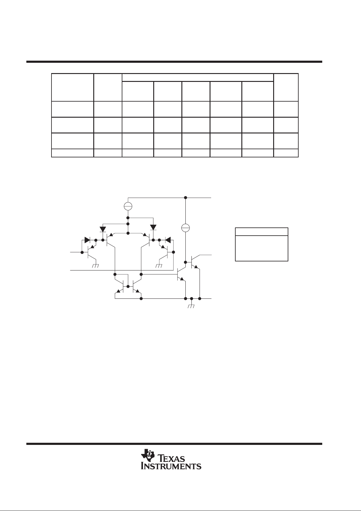
schematic (each comparator)
80-µA
Current Regulator
80 µA
60 µA
10 µA
V
CC
10 µA
OUT
GND
IN+
IN–
Epi-FET
Diodes
Resistors
Transistors
Current values shown are nominal.
COMPONENT COUNT
1
2
2
30

LM193, LM293, LM293A, LM393
LM393A, LM393Y, LM2903, LM2903Q
DUAL DIFFERENTIAL COMPARATORS
SLCS005E – JUNE 1976 – REVISED NOVEMBER 1999
3
POST OFFICE BOX 655303 • DALLAS, TEXAS 75265
absolute maximum ratings over operating free-air temperature range (unless otherwise noted)
†
Supply voltage, VCC (see Note 1) 36 V. . . . . . . . . . . . . . . . . . . . . . . . . . . . . . . . . . . . . . . . . . . . . . . . . . . . . . . . . . . .
Differential input voltage, VID (see Note 2) ±36 V. . . . . . . . . . . . . . . . . . . . . . . . . . . . . . . . . . . . . . . . . . . . . . . . . . .
Input voltage range, VI (either input) –0.3 V to 36 V. . . . . . . . . . . . . . . . . . . . . . . . . . . . . . . . . . . . . . . . . . . . . . . . .
Output voltage, V
O
36 V. . . . . . . . . . . . . . . . . . . . . . . . . . . . . . . . . . . . . . . . . . . . . . . . . . . . . . . . . . . . . . . . . . . . . . . . .
Output current, IO 20 mA. . . . . . . . . . . . . . . . . . . . . . . . . . . . . . . . . . . . . . . . . . . . . . . . . . . . . . . . . . . . . . . . . . . . . . . .
Duration of output short-circuit to ground (see Note 3) Unlimited. . . . . . . . . . . . . . . . . . . . . . . . . . . . . . . . . . . . . .
Continuous total power dissipation See Dissipation Rating Table. . . . . . . . . . . . . . . . . . . . . . . . . . . . . . . . . . . . .
Package thermal impedance, θJA (see Note 4): D package 97°C/W. . . . . . . . . . . . . . . . . . . . . . . . . . . . . . . . . . .
P package 85°C/W. . . . . . . . . . . . . . . . . . . . . . . . . . . . . . . . . . .
PW package 149°C/W. . . . . . . . . . . . . . . . . . . . . . . . . . . . . . . .
Case temperature for 60 seconds: FK package 260°C. . . . . . . . . . . . . . . . . . . . . . . . . . . . . . . . . . . . . . . . . . . . . .
Lead temperature 1,6 mm (1/16 inch) from case for 10 seconds: D, P, or PW package 260°C. . . . . . . . . . . .
Lead temperature 1,6 mm (1/16 inch) from case for 60 seconds: JG package 300°C. . . . . . . . . . . . . . . . . . . .
Storage temperature range, T
stg
–65°C to 150°C. . . . . . . . . . . . . . . . . . . . . . . . . . . . . . . . . . . . . . . . . . . . . . . . . . .
†
Stresses beyond those listed under “absolute maximum ratings” may cause permanent damage to the device. These are stress ratings only, and
functional operation of the device at these or any other conditions beyond those indicated under “recommended operating conditions” is not
implied. Exposure to absolute-maximum-rated conditions for extended periods may affect device reliability.
NOTES: 1. All voltage values, except differential voltages, are with respect to the network ground.
2. Differential voltages are at IN+ with respect to IN–.
3. Short circuits from outputs to VCC can cause excessive heating and eventual destruction.
4. The package thermal impedance is calculated in accordance with JESD 51.
DISSIPATION RATING TABLE
PACKAGE
TA ≤ 25°C
POWER RATING
DERATING
FACTOR
DERATE
ABOVE T
A
TA = 70°C
POWER RATING
TA = 85°C
POWER RATING
TA = 125°C
POWER RATING
FK 900 mW 11.0 mW/°C 68°C 880 mW 715 mW 275 mW
JG 900 mW 8.4 mW/°C 43°C 672 mW 546 mW 210 mW
 Loading...