

查询LM101AD供应商
LM101A, LM201A, LM301A
HIGH-PERFORMANCE OPERATIONAL AMPLIFIERS
D961, OCTOBER 1979 – REVISED SEPTEMBER 1990
• Low Input Currents
• Low Input Offset Parameters
• Frequency and Transient Response
Characteristics Adjustable
• Short-Circuit Protection
• Offset-Voltage Null Capability
• No Latch-Up
• Wide Common-Mode and Differential
Voltage Ranges
• Same Pin Assignments as uA709
• Designed to be Interchangeable with
National Semiconductor LM101A and
LM301A
description
The LM101A, LM201A, and LM301A are highperformance operational amplifiers featuring very
low input bias current and input offset voltage and
current to improve the accuracy of highimpedance circuits using these devices. The high
common-mode input voltage range and the
absence of latch-up make these amplifiers ideal
for voltage-follower applications. The devices are
protected to withstand short circuits at the output.
The external compensation of these amplifiers
allows the changing of the frequency response
(when the closed-loop gain is greater then unity)
for applications requiring wider bandwidth or
higher slew rate. A potentiometer may be
connected between the offset-null inputs (N1 and
N2), as shown in Figure 7, to null out the offset
voltage.
The LM101A is characterized for operation over
the full military temperature range of –55°C to
125°C, the LM201A is characterized for operation
from –25°C to 85°C, and the LM301A is
characterized for operation from 0°C to 70°C.
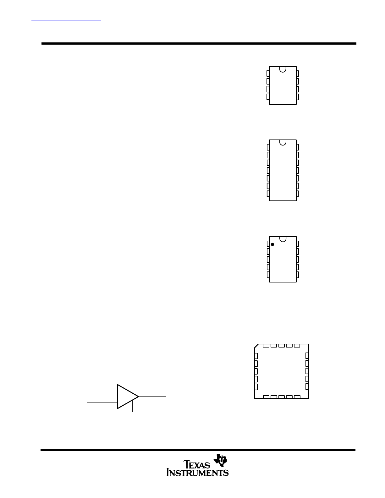
symbol
Noninverting
Input IN+
Inverting
Input IN–
+
–
N2
N1/
COMP
Output
D, JG, OR P PACKAGE
(T0P VIEW)
N1/COMP
V
N1/COMP
V
N1/COMP
V
FK CHIP-CARRIER PACKAGE
NC
IN–
NC
IN+
NC
NC – No internal connection
1
IN–
2
IN+
3
4
CC–
LM101A
W FLAT PACKAGE
(T0P VIEW)
NC
1
NC
2
3
IN–
4
IN+
5
6
CC–
NC
7
LM101A
U FLAT PACKAGE
(T0P VIEW)
NC
1
2
IN–
3
IN+
4
5
CC–
LM101A
(T0P VIEW)
NC
N1/COMP
NC
3212019
4
5
6
7
8
910111213
NCVNC
CC –
8
7
6
5
14
13
12
11
10
9
8
10
9
8
7
6
COMP
N2
COMP
V
CC+
OUT
OFFSET N2
NC
NC
COMP
V
CC+
OUT
OFFSET N2
NC
NC
COMP
V
CC+
OUT
OFFSET N2
NC
NC
18
V
17
CC+
NC
16
OUT
15
NC
14
NC
PRODUCTION DATA information is current as of publication date.
Products conform to specifications per the terms of Texas Instruments
standard warranty. Production processing does not necessarily include
testing of all parameters.
POST OFFICE BOX 655303 • DALLAS, TEXAS 75265
Copyright 1991, Texas Instruments Incorporated
2–1
LM101A, LM201A, LM301A
HIGH-PERFORMANCE OPERATIONAL AMPLIFIERS
AVAILABLE OPTIONS
T
A
0°C to 70°C 7.5 mV LM301AD – – LM301AP – –
–25°C to 85°C 2 mV LM201AD – – LM201AP – –
–55°C to 125°C 2 mV LM101AD LM101AFK LM101AJG LM101AP LM101AU LM101AW
The D package is available taped and reeled. Add the suffix R to the device type, (i.e., LM301ADR).
VIO MAX
at 25°C
SMALL OUTLINE CHIP CARRIER CERAMIC DIP PLASTIC DIP FLAT
(D) (FK) (JG) (P) (U) (W)
absolute maximum ratings over operating free-air temperature range (unless otherwise noted)
Supply voltage V
Supply voltage V
Differential input voltage (see Note 2) ±30 ±30 ±30 V
Input voltage (either input, see Notes 1 and 3) ±15 ±15 ±15 V
Voltage between either offset null terminal (N1/N2) and V
Duration of output short-circuit (see Note 4) unlimited unlimited unlimited
Continuous total power dissipation See Dissipation Rating Table
Operating free-air temperature range –55 to125 –25 to85 0to70 °C
Storage temperature range –65 to150 –65 to150 –65 to150 °C
Case temperature for 60 seconds: FK package 260 °C
Lead temperature 1,6 mm (1/16 inch) from case for 60 seconds JG, U, or W package 300 °C
Lead temperature 1,6 mm (1/16 inch) from case for 10 seconds D or P package 260 260 260 °C
NOTES: 1. All voltage values, unless otherwise noted, are with respect to the midpoint between V
2. Dif ferential voltages are at the noninverting input terminal with respect to the inverting input terminal.
3. The magnitude of the input voltage must never exceed the magnitude of the supply voltage or 15 V, whichever is less.
4. The output may be shorted to ground or either power supply. For the LM101A only , the unlimited duration of the short-circuit applies
at (or above) 125°C case temperature or 75°C free-air temperature. For the LM201A only, the unlimited duration of the short-circuit
applies at (or below) 85°C case temperatuare or 75°C free-air temperature.
(see Note 1) 22 22 18 V
CC+
(see Note 1) –22 –22 –18 V
CC–
CC–
PACKAGE
FLAT PACK
PACK
LM101A LM201A LM301A UNIT
–0.5 to 2 –0.5 to 2 –0.5 to 2 V
CC+
and V
CC–
.
DISSIPATION RATING TABLE
PACKAGE
D 500 mW 5.8 mW/°C 64°C 464 mW 377 mW 145 mW
FK 500 mW 11.0 mW/°C 105°C 500 mW 500 mW 275 mW
JG 500 mW 8.4 mW/°C90°C 500 mW 500 mW 210 mW
P 500 mW 8.0 mW/°C87°C 500 mW 500 mW 200 mW
U 500 mW 5.4 mW/°C57°C 432 mW 351 mW 135 mW
W 500 mW 8.0 mW/°C 87°C 500 mW 500 mW 200 mW
TA ≤ 25°C DERATING DERATE TA = 70°C TA = 85°C TA = 125°C
POWER RATING FACTOR ABOVE T
POWER RATING POWER RATING POWER RATING
A
recommended operating conditions
MIN MAX UNIT
Supply voltage, V
Supply voltage, V
CC+
CC–
5 18
–5 –18
V
2–2
POST OFFICE BOX 655303 • DALLAS, TEXAS 75265
LM101A, LM201A, LM301A
HIGH-PERFORMANCE OPERATIONAL AMPLIFIERS
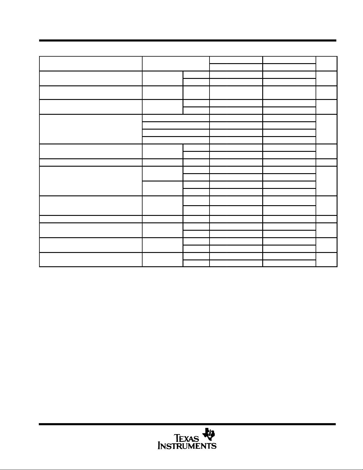
electrical characteristics at specified free-air temperature, CC = 30 pF (see Note 5)
PARAMETER TEST CONDITIONS
IO
VIO
IO nA
α
IIO nA/°C
I
IB
V
ICR
V
OPP
A
VD
r
i
CMRR Common-mode rejection ratio
k
SVR
I
CC
†
All characteristics are measured under open-loop conditions with zero common-mode input voltage unless otherwise specified. Full range for
LM101A is –55°C to 125°C, for LM201A is –25°C to 85°C, and for LM301A is 0°C to 70°C.
NOTES: 5. Unless otherwise noted, V
Input offset voltage VO = 0
Average temperature coefficient of
input offset voltage
Input offset currentI
TA = –55°C to 25°C 0.02 0.2
Average temperature coefficient of TA = 25°C to MAX 0.01 0.1
input offset current TA = 0°C to 25°C 0.02 0.6
TA = 25°C to 70°C 0.01 0.3
Input bias current
Common-mode input voltage range See Note 6 Full range ±15 ±12 V
V
= ±15 V, 25°C 24 28 24 28
CC±
Maximum peak-to-peak output RL = 10 kΩ Full range 24 24
voltage swing V
Large-signal differential voltage
amplification
Input resistance 25°C 1.5 4 0.5 2 MΩ
Supply voltage rejection ratio 25°C 80 98 70 96
(∆ VCC/∆ VIO) Full range 80 70
Supply current
= ±5 V to ±20 V for LM101A and LM201A, and V
are at V
6. For LM101A and LM201A, V
CC±
= ±15 V.
CC±
= ±20 V. For LM301A, V
CC±
= ±15 V, 25°C 20 26 20 26
CC±
RL = 2 kΩ Full range 20 20
V
= ±15 V,
CC±
VO = ±10 V,
RL ≥ 2 kΩ
VIC = V
No load, VO = 0, 25°C 1.8 3 1.8 3
See Note 6 MAX 1.2 2.5
ICR
min
†
25°C 0.6 2 2 7.5
Full range 3 10
Full rangeVO = 0α
25°C 1.5 10 3 50
Full range 20 70
25°C 30 75 70 250
Full range 100 300
25°C
Full range
25°C 80 98 70 90
Full range 80 70
= ±15 V.
CC±
LM101A, LM201A LM301A
MIN TYP MAX MIN TYP MAX
315 630µV/°C
50 200 25 200
25
= ±5 V to ±15 V for LM301A. All typical values
CC±
15
UNIT
mVV
nA
V
V/mV
dB
dB
mA
POST OFFICE BOX 655303 • DALLAS, TEXAS 75265
2–3

LM101A, LM201A, LM301A
HIGH-PERFORMANCE OPERATIONAL AMPLIFIERS
TYPICAL CHARACTERISTICS
INPUT OFFSET CURRENT
FREE-AIR TEMPERATURE
4
VCC ± = ±15 V
3
2I
– Input Offset Current – nA
1
IO
I
0
–7 –50 –25 0 25 50
TA – Free-Air Temperature – ° C
Figure 1 Figure 2
vs
LM101A
LM201A
LM301A
75 100 125
INPUT BIAS CURRENT
FREE-AIR TEMPERATURE
100
VCC ± = ±15 V
80
60
40
– Input Bias Current – nAI
IB
20
0
–75 –50 –25 0 25 50
TA – Free-Air Temperature – ° C
vs
LM301A
LM101A
LM201A
75 100 125
MAXIMUM PEAK-TO-PEAK OUTPUT
VOLTAGE
(WITH SINGLE-POLE COMPENSATION)
vs
30
28
24
20
16
12
8
– Maximum Peak-to-Peak Output Voltage – V
OPP
V
CC = 30 pF
4
0
1 k 10 k 100 k 1 M 10 M
FREQUENCY
VCC ± = ±15 V
RL = 10 KΩ
TA = 25°C
CC = 3 pF
f – Frequency – Hz
Figure 3 Figure 4
OPEN-LOOP LARGE-SIGNAL DIFFERENTIAL
VOLTAGE AMPLIFICATION
vs
SUPPLY VOLTAGE
400
R
= 2 KΩ
L
TA = 25°C
200
100
40
20
– Differential Voltage Amplification – V/mV
VD
A
10
04810121620
| V
| – Supply Voltage – V
CC±
LM301A
LM101A
LM201A
14 1826
2–4
POST OFFICE BOX 655303 • DALLAS, TEXAS 75265

TYPICAL CHARACTERISTICS
OPEN-LOOP LARGE-SIGNAL DIFFERENTIAL
VOLTAGE AMPLIFICATION
vs
FREQUENCY
VCC ± = ±15 V
RL = 2 kΩ
CC = 30 pF
TA = 25°C
10
10
10
10
10
7
6
5
4
3
LM101A, LM201A, LM301A
HIGH-PERFORMANCE OPERATIONAL AMPLIFIERS
VOLTAGE-FOLLOWER
LARGE-SIGNAL PULSE RESPONSE
8
VCC ± = ±15 V
6
4
2
0
Output
RL = 2 kΩ
CL = 100 pF
CC = 30 pF
TA = 25°C
2
10
1
10
– Differential Voltage Amplification
VD
1
A
10–1
1 10 100 1 k 10 k 100 k
V
I
R1
R3
f – Frequency – Hz
1 M 10 M 100 M
–2
–4
Input and Output Voltages – V
–6
–8
0 10203040
Input
t – Time – µs
Figure 5 Figure 6
TYPICAL APPLICATION DATA
R2
V
O
V
I
CCw
R3
+*
R1@30 pF
R1)R2
R1@R2
+
R1)R2
R2
R1
–
+
V
CC+
V
O
RL ≥ 2 kΩ
50 60 90
70 80
V
CC–
COMP
C
C
N1
5 MΩ
5.1 MΩ
N2
Figure 7. Inverting Circuit with Adjustable Gain, Single-Pole Compensation,
and Offset Adjustment
POST OFFICE BOX 655303 • DALLAS, TEXAS 75265
2–5

LM101A, LM201A, LM301A
HIGH-PERFORMANCE OPERATIONAL AMPLIFIERS
2–6
POST OFFICE BOX 655303 • DALLAS, TEXAS 75265

IMPORTANT NOTICE
T exas Instruments (TI) reserves the right to make changes to its products or to discontinue any semiconductor
product or service without notice, and advises its customers to obtain the latest version of relevant information
to verify, before placing orders, that the information being relied on is current.
TI warrants performance of its semiconductor products and related software to the specifications applicable at
the time of sale in accordance with TI’s standard warranty. Testing and other quality control techniques are
utilized to the extent TI deems necessary to support this warranty. Specific testing of all parameters of each
device is not necessarily performed, except those mandated by government requirements.
Certain applications using semiconductor products may involve potential risks of death, personal injury, or
severe property or environmental damage (“Critical Applications”).
TI SEMICONDUCTOR PRODUCTS ARE NOT DESIGNED, INTENDED, AUTHORIZED, OR WARRANTED
TO BE SUITABLE FOR USE IN LIFE-SUPPORT APPLICATIONS, DEVICES OR SYSTEMS OR OTHER
CRITICAL APPLICATIONS.
Inclusion of TI products in such applications is understood to be fully at the risk of the customer. Use of TI
products in such applications requires the written approval of an appropriate TI officer . Questions concerning
potential risk applications should be directed to TI through a local SC sales office.
In order to minimize risks associated with the customer’s applications, adequate design and operating
safeguards should be provided by the customer to minimize inherent or procedural hazards.
TI assumes no liability for applications assistance, customer product design, software performance, or
infringement of patents or services described herein. Nor does TI warrant or represent that any license, either
express or implied, is granted under any patent right, copyright, mask work right, or other intellectual property
right of TI covering or relating to any combination, machine, or process in which such semiconductor products
or services might be or are used.
Copyright 1996, Texas Instruments Incorporated
 Loading...