

®
IVC102
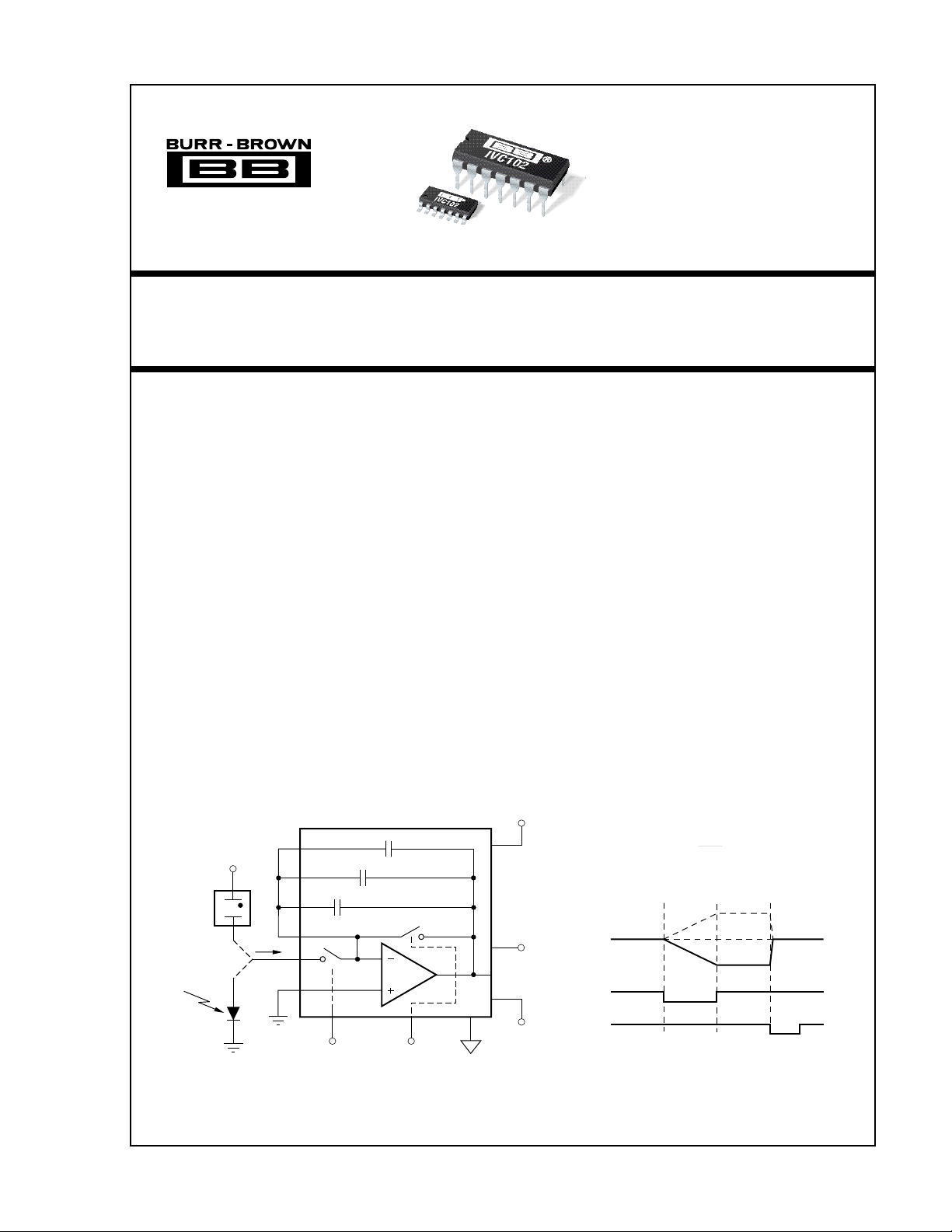
PRECISION SWITCHED INTEGRATOR
TRANSIMPEDANCE AMPLIFIER
APPLICA TIONS
● PRECISION LOW CURRENT MEASUREMENT
● PHOTODIODE MEASUREMENTS
● IONIZATION CHAMBER MEASUREMENTS
● CURRENT/CHARGE-OUTPUT SENSORS
● LEAKAGE CURRENT MEASUREMENT
FEATURES
● ON-CHIP INTEGRATING CAPACITORS
● GAIN PROGRAMMED BY TIMING
● LOW INPUT BIAS CURRENT: 750fA max
● LOW NOISE
● LOW SWITCH CHARGE INJECTION
● FAST PULSE INTEGRATION
● LOW NONLINEARITY: 0.005% typ
● 14-PIN DIP, SO-14 SURFACE MOUNT
60pF
C
3
C
30pF
2
10pF
1
S
2
S
1
11 12 13
S
1
S
2
Ionization
Chamber
Photodiode
I
IN
Analog
Ground
6
5
C
4
3
2
1
Logic Low closes switches
V
B
DESCRIPTION
The IVC102 is a precision integrating amplifier with
FET op amp, integrating capacitors, and low leakage
FET switches. It integrates low-level input current for
a user-determined period, storing the resulting voltage
on the integrating capacitor. The output voltage can be
held for accurate measurement. The IVC102 provides
a precision, lower noise alternative to conventional
transimpedance op amp circuits that require a very
high value feedback resistor.
The IVC102 is ideal for amplifying low-level sensor
currents from photodiodes and ionization chambers.
The input signal current can be positive or negative.
TTL/CMOS-compatible timing inputs control the integration period, hold and reset functions to set the
effective transimpedance gain and to reset (discharge)
the integrator capacitor.
Package options include 14-Pin plastic DIP and SO-14
surface-mount packages. Both are specified for the
–40°C to 85°C industrial temperature range.
V+
14
10
9
Digital
Ground
V–
V
O
0V
Hold Integrate Hold Reset
S
1
S
2
–1
=
V
O
Positive or Negative
Signal Integration
IIN(t)
∫
C
INT
dt
SBFS009
International Airport Industrial Park • Mailing Address: PO Box 11400 • Tucson, AZ 85734 • Street Address: 6730 S. Tucson Blvd. • Tucson, AZ 85706
Tel: (520) 746-1111 • Twx: 910-952-1111 • Cable: BBRCORP • Telex: 066-6491 • FAX: (520) 889-1510 • Immediate Product Info: (800) 548-6132
© 1996 Burr-Brown Corporation PDS-1329A Printed in U.S.A. June, 1996
1
IVC102
®

SPECIFICATIONS
At TA = +25°C, VS = ±15V, RL = 2kΩ, C
= C1 + C2 + C3, 1ms integration period
INT
PARAMETER CONDITIONS MIN TYP MAX UNITS
TRANSFER FUNCTION V
Gain Error C
vs Temperature ±25 ppm/°C
= C1 + C2 + C
INT
Nonlinearity V
Input Current Range ±100 µA
Offset Voltage
(2)
IIN = 0, CIN = 50pF –5 ±20 mV
vs Temperature ±30 µV/°C
vs Power Supply V
Droop Rate, Hold Mode –1 nV/µs
= +4.75/–10 to +18/–18V 150 750 µV/V
S
OP AMP
Input Bias Current S
vs Temperature See Typical Curve
Offset Voltage (Op Amp V
vs Temperature ±5 µV/°C
vs Power Supply V
Noise Voltage f = 1kHz 10 nV/√Hz
) ±0.5 ±5mV
OS
= +4.75/–10 to +18/–18V 10 100 µV/V
S
INTEGRATION CAPACITORS
C
+ C2 + C
1
C
1
C
2
C
3
3
vs Temperature ±25 ppm/°C
OUTPUT
Voltage Range, Positive R
Negative R
Short-Circuit Current ±20 mA
Capacitive Load Drive 500 pF
Noise Voltage See Typical Curve
DYNAMIC CHARACTERISTIC
Op Amp Gain-Bandwidth 2 MHz
Op Amp Slew Rate 3V/µs
Reset
Slew Rate 3V/µs
Settling Time, 0.01% 10V Step 6 µs
DIGITAL INPUTS (TTL/CMOS Compatible)
V
(referred to digital ground) (Logic High) 2 5.5 V
IH
V
(referred to digital ground) (Logic Low) –0.5 0.8 V
IL
I
IH
I
IL
Switching Time 100 ns
POWER SUPPLY
Voltage Range: Positive +4.75 +15 +18 V
Negative –10 –15 –18 V
Current: Positive 4.1 5.5 mA
Negative –1.6 –2.2 mA
Analog Ground –0.2 mA
Digital Ground –2.3 mA
TEMPERATURE RANGE
Operating Range –40 85 °C
Storage –55 125 °C
Thermal Resistance,
DIP 100 °C/W
θ
JA
SO-14 150 °C/W
NOTES: (1) Standard test timing: 1ms integration, 200µs hold, 100µs reset. (2) Hold mode output voltage after 1ms integration of zero input current. Includes op
amp offset voltage, integration of input error current and switch charge injection effects.
(1)
, unless otherwise specified.
IVC102P, U
= –(IIN)(T
3
= ±10V ±0.005 %
O
, S2 Open –100 ±750 fA
1
O
)/C
INT
INT
±5 +25/–17 %
80 100 120 pF
10 pF
30 pF
60 pF
= 2kΩ (V+)–3 (V+)–1.3 V
L
= 2kΩ (V–)+3 (V–)+2.6 V
L
VIH = 5V 2 µA
VIL = 0V 0 µA
The information provided herein is believed to be reliable; however, BURR-BROWN assumes no responsibility for inaccuracies or omissions. BURR-BROWN assumes
no responsibility for the use of this information, and all use of such information shall be entirely at the user’s own risk. Prices and specifications are subject to change
without notice. No patent rights or licenses to any of the circuits described herein are implied or granted to any third party. BURR-BROWN does not authorize or warrant
any BURR-BROWN product for use in life support devices and/or systems.
®
IVC102
2
ABSOLUTE MAXIMUM RATINGS
Supply Voltage, V+ to V– .................................................................... 36V
Logic Input Voltage ...................................................................... V– to V+
Output Short Circuit to Ground ............................................... Continuous
Operating Temperature ................................................. –40°C to +125°C
Storage Temperature..................................................... –55°C to +125°C
Lead Temperature (soldering, 10s) ................................................. 300° C
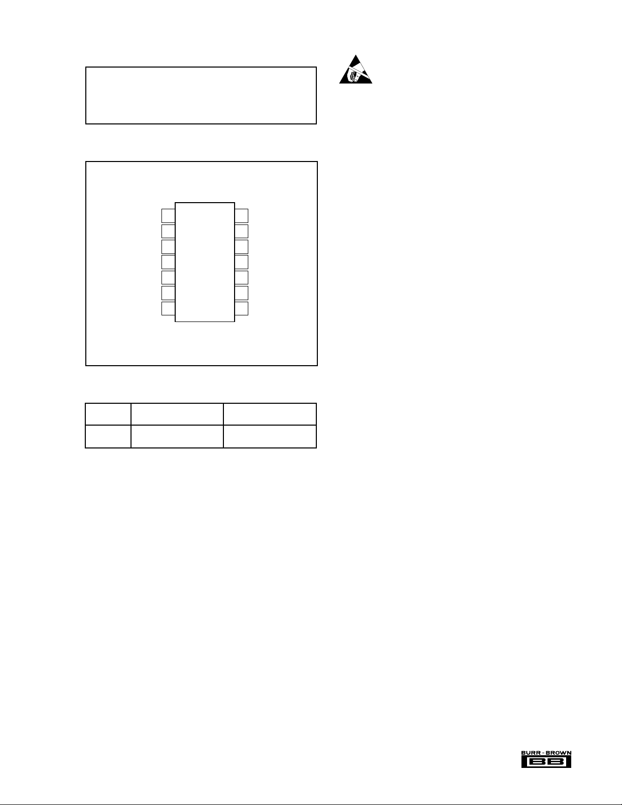
PIN CONNECTIONS
Top View 14-Pin DIP/
SO-14 Surface Mount
ELECTROSTATIC
DISCHARGE SENSITIVITY
This integrated circuit can be damaged by ESD. Burr-Brown
recommends that all integrated circuits be handled with
appropriate precautions. Failure to observe proper handling
and installation procedures can cause damage.
ESD damage can range from subtle performance degradation to complete device failure. Precision integrated circuits
may be more susceptible to damage because very small
parametric changes could cause the device not to meet its
published specifications.
14
V+
13
Digital Ground
12
S
2
11
S
1
10
V
O
9
V–
8
NC
–In
C
NC
1
2
I
IN
3
4
C
1
5
C
2
6
3
7
Analog Ground
NC = No Internal Connection
Connect to Analog Ground for Lowest Noise
PACKAGE INFORMATION
PRODUCT PACKAGE NUMBER
PACKAGE DRAWING
IVC102P 14-Pin DIP 010
IVC102U SO-14 Surface Mount 235
NOTE: (1) For detailed drawing and dimension table, please see end of data
sheet, or Appendix D of Burr-Brown IC Data Book.
(1)
®
3
IVC102
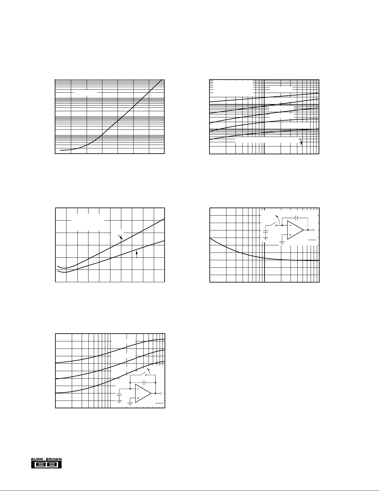
TYPICAL PERFORMANCE CURVES
At TA = +25°C, VS = ±15V, RL = 2kΩ, C
= C1 + C2 + C3, 1ms integration period, unless otherwise specified.
INT
100p
INPUT BIAS CURRENT vs TEMPERATURE
S1, S2 Open
10p
1p
100f
Input Bias Current (A)
10f
–50 –25 0 25 50 75 100 125
Temperature (°C)
30
RESET TIME vs C
25
Time Required to
Reset from ±10V
INT
to 0V.
20
0.01%
15
10
Reset Time (µs)
1%
5
0
0 100 200 300 400 500 600 700 800 900 1000
C
(pF)
INT
1000
rms Variation
of 100 Measurement
Cycles, T
100
10
Noise Voltage (µVrms)
TOTAL OUTPUT NOISE vs C
INT
= 1ms.
C
C
C
C
Reset Mode, S1 Open, S2 Closed.
INT
INT
INT
INT
= 10pF
= 30pF
= 100pF
= 300pF
C
INT
IN
= 1000pF
1
10 100 1000
C
(pF)
IN
CHARGE INJECTION vs INPUT CAPACITANCE
S
2.0
1
1.8
S
1.6
1.4
1
C
IN
1.2
1.0
0.8
0.6
Charge Injection, ∆Q (pC)
0.4
0.2
0
10 100 1000
Input Capacitance, C
IN
(pF)
100pF
∆V
∆Q
=
O
100pF
CHARGE INJECTION vs INPUT CAPACITANCE
S
1.0
0.9
2
(V+) = +18V
0.8
0.7
(V+) = +15V
0.6
0.5
0.4
(V+) = +4.75V
S
2
100pF
0.3
Charge Injection, ∆Q (pC)
0.2
C
IN
0.1
0
10 100 1000
Input Capacitance, C
®
IN
(pF)
IVC102
∆V
∆Q
=
O
100pF
4

APPLICATION INFORMATION
Figure 1 shows the basic circuit connections to operate the
IVC102. Bypass capacitors are shown connected to the
power supply pins. Noisy power supplies should be avoided
or decoupled and carefully bypassed.
The Analog Ground terminal, pin 1, is shown internally
connected to the non-inverting input of the op amp. This
terminal connects to other internal circuitry and should be
connected to ground. Approximately 200µA flows out of
this terminal.
Digital Ground, pin 13, should be at the same voltage
potential as analog ground (within 100mV). Analog and
Digital grounds should be connected at some point in the
system, usually at the power supply connections to the
circuit board. A separate Digital Ground is provided so that
noisy logic signals can be referenced to separate circuit
board traces.
Integrator capacitors C
parallel for a total C
for a wide variety of integrating current measurements. The
input signal connections and control timing and C
will depend on the sensor or signal type and other application details.
, C2 and C3 are shown connected in
1
= 100pF. The IVC102 can be used
INT
INT
value
BASIC RESET-AND-INTEGRATE MEASUREMENT
Figure 1 shows the circuit and timing for a simple reset-andintegrate measurement. The input current is connected directly to the inverting input of the IVC102, pin 3. Input
current is shown flowing out of pin 3, which produces a
positive-going ramp at V
. Current flowing into pin 3 would
O
produce a negative-going ramp.
A measurement cycle starts by resetting the integrator output
voltage to 0V by closing S
current begins when S
charge C
. VO is measured with a sampling a/d converter
INT
for 10µs. Integration of the input
2
opens and the input current begins to
2
at the end of an integration period, just prior to the next reset
period. The ideal result is proportional to the average input
current (or total accumulated charge).
Switch S
is again closed to reset the integrator output to 0V
2
before the next integration period.
This simple measurement arrangement is suited to many
applications. There are, however, limitations to this basic
approach. Input current continues to flow through S
the reset period. This leaves a small voltage on C
to the input current times R
, the on-resistance of S2,
S2
during
2
equal
INT
approximately 1.5kΩ.
0V
Op Amp V
+
• R
I
IN
Figure 1a
Photodiode
Charge Injection
of S
2
OS
S2
V
O
0V
I
IN
T
Analog
Ground
1
V+
+15V
0.1µF
Digital
Ground
14
10 V
9
–15V
V–
O
0.1µF
Sampling
A/D
Converter
Digital
Data
60pF
6
5
C
4
3
2
1
Logic
(+5V)
C
3
C
30pF
2
10pF
1
S
2
S
1
11 12 13
S
High
2
See timing
signal below
Figure 1b
T
2
Integrate
S
2
10µs
Reset
FIGURE 1. Reset-and Integrate Connections and Timing.
(S
Open)
2
5
10µs
Reset
®
IVC102

In addition, the offset voltage of the internal op amp and
charge injection of S
contribute to the voltage on C
2
INT
at the
start of integration.
Performance of this basic approach can be improved by
sampling V
after the reset period at T1 and subtracting this
O
measurement from the final sample at T
voltage, charge injection effects and I•R
are removed with this two-point measurement. The effec-
S
2
S2
tive integration period is the time between the two measurements, T
2-T1
.
COMPARISON TO CONVENTIONAL TRANSIMPEDANCE AMPLIFIERS
. Op amp offset
2
offset voltage on
With the conventional transimpedance amplifier circuit
of Figure 2a, input current flows through the feedback
resistor, R
, to create a proportional output voltage.
F
= –IIN R
V
O
F
The transimpedance gain is determined by RF. Very large
values of R
are required to measure very small signal
F
current. Feedback resistor values exceeding 100MΩ are
common.
The IVC102 (Figure 2b) provides a similar function,
converting an input current to an output voltage. The
input current flows through the feedback capacitor, C
INT
charging it at a rate that is proportional to the input
current. With a constant input current, the IVC102’s
output voltage is
= –IIN T
V
O
after an integration time of T
INT/CINT
.
INT
Conventional Transimpedance Amplifier
Figure 2a
I
IN
R
F
V
is proportional to the integration time, T
O
inversely proportional to the feedback capacitor, C
The effective transimpedance gain is T
INT/CINT
INT
, and
INT
. Ex-
.
tremely high gain that would be impractical to achieve
with a conventional transimpedance amplifier can be
achieved with small integration capacitor values and/or
long integration times. For example the IVC102 with
= 100pF and T
C
INT
= 100ms provides an effective
INT
transimpedance of 1GΩ. A 10nA input current would
produce a 10V output after 100ms integration.
,
The integrating behavior of the IVC102 reduces noise by
averaging the input noise of the sensor, amplifier, and
external sources.
Integrating Transimpedance Amplifier
Figure 2b
I
IN
C
INT
V
O
VO = –IIN R
Provides time-continuous output
voltage proportional to I
.
IN
F
FIGURE 2. Comparison to a Conventional Transimpedance Amplifier.
CURRENT-OUTPUT SENSORS
Figure 3 shows a model for many current-output sensors
such as photodiodes and ionization chambers. Sensor output
is a signal-dependent current with a very high source resistance. The output is generally loaded into a low impedance
®
IVC102
so that the terminal voltage is kept very low. Typical sensor
capacitance values range from 10pF to over 100pF. This
capacitance plays a key role in operation of the switchedinput measurement technique (see next section).
6
–1
=
V
O
C
INT
for constant IIN, at the end of T
VO = –I
Output voltage after integration period is
proportional to average I
the period.
IN
T
IN
C
throughout
∫
V
IIN(t)
INT
INT
O
dt
INT

3a
3b
Photodiode
Sensor
I
I: Signal - Dependent Current
R: Sensor Resistance
C: Sensor Capacitance
0V
V
O
RC
A
6
5
C
4
1
3
2
1
S
Charge transferred
from sensor C
.
to C
INT
C
C
30pF
2
10pF
S
1
11
1
See timing
signals below
60pF
3
S
2
12 13
S
2
Effective
Signal Integration
Period, T
VO waveform with
approx. half-scale input current.
V+
+15V
14
10 V
9
–15V
V–
S
0.1µF
O
0.1µF
A/D
Converter
Digital
Data
0V
B
(S1 Open) (S1 Closed)
10µs
10µs
Reset
Op Amp
V
OS
S
10µs
Pre-Int.
Hold
∆Q
Opening
2
A
Hold
(S
Open)
2
waveform with
V
O
zero input current.
∆Q
Closing
S
1
3c
S
1
S
2
+10mV
0V
V
O
–10mV
FIGURE 3. Switched-Input Measurement Technique.
SWITCHED-INPUT MEASUREMENT TECHNIQUE
While the basic reset-and-integrate measurement arrangement in Figure 1 is satisfactory for many applications, the
switched-input timing technique shown in Figure 3 has
important advantages. This method can provide continuous
integration of the input signal. Furthermore, it can hold the
output voltage constant after integration for stable conversion (desirable for a/d converter without a sample/hold).
10µs
10µs
Hold
Reset
Transfer Function
Offset Voltage
Ramp due to
input bias current
(exaggerated).
Opening
S
1
∆Q
B
Input connections and timing are shown in Figure 3.
The timing diagram, Figure 3b, shows that S
when S
is open. During the short period that S1 is open
2
is closed only
1
(30µs in this timing example), any signal current produced
by the sensor will charge the sensor’s source capacitance.
This charge is then transferred to C
when S1 is closed. As
INT
a result, no charge produced by the sensor is lost and the
input signal is continuously integrated. Even fast input
pulses are accurately integrated.
7
IVC102
0V
®

The input current, IIN, is shown as a conventional current
flowing into pin 2 in this diagram but the input current could
be bipolar (positive or negative). Current flowing out of pin
2 would produce a positive-ramping V
.
O
The timing sequence proceeds as follows:
Reset Period
The integrator is reset by closing switch S
with S1 open. A
2
10µs reset time is recommended to allow the op amp to slew
to 0V and settle to its final value.
Pre-Integration Hold
is opened, holding VO constant for 10µs prior to integra-
S
2
tion. This pre-integration hold period assures that S
open before S
is closed so that no input signal is lost. A
1
is fully
2
minimum of 1µs is recommended to avoid switching overlap. The 10µs hold period shown in Figure 3b also allows an
a/d converter measurement to be made at point A. The
purpose of this measurement at A is discussed in the “Offset
Errors” section.
Integration on C
Integration of the input current on C
INT
begins when S1 is
INT
closed. An immediate step output voltage change occurs as
the charge that was stored on the input sensor capacitance is
transferred to C
. Although this period of charging C
INT
INT
occurs only while S1 is closed, the charge transferred as S
is closed causes the effective integration time to be equal to
the complete conversion period—see Figure 3b.
The integration period could range from 100µs to many
minutes, depending on the input current and C
While S
is closed, IIN charges C
1
, producing a negative-
INT
going ramp at the integrator output voltage, V
value.
INT
. The output
O
voltage at the end of integration is proportional to the
average input current throughout the complete conversion
cycle, including the integration period, reset and both hold
periods.
Hold Period
Opening S
after S
halts integration on C
1
is opened, the output voltage is stable and can be
1
. Approximately 5µs
INT
measured (at point B). The hold period is 10µs in this
example. C
remains charged until a S2 is again closed, to
INT
reset for the next conversion cycle.
In this timing example, S
is open for a total of 30µs. During
1
this time, signal current from the sensor charges the sensor
source capacitance. Care should be used to assure that the
voltage developed on the sensor does not exceed approximately 200mV during this time. The I
terminal, pin 2, is
IN
internally clamped with diodes. If these diodes forward bias,
signal current will flow to ground and will not be accurately
integrated.
A maximum of 333nA signal current could be accurately
integrated on a 50pF sensor capacitance for 30µs before
200mV would be developed on the sensor.
= (50pF) (200mV) / 30µs = 333nA
I
MAX
OFFSET ERRORS
Figure 3c shows the effect on V
due to op amp input offset
O
voltage, input bias current and switch charge injection. It
assumes zero input current from the sensor. The various
offsets and charge injection (∆Q) jumps shown are typical of
that seen with a 50pF source capacitance. The specified
“transfer function offset voltage” is the voltage measured
during the hold period at B. Transfer function offset voltage
is dominated by the charge injection of S
amp V
. The opening and closing charge injections of S
OS
opening and op
2
are very nearly equal and opposite and are not significant
contributors.
Note that using a two-point difference measurement at A
and B can dramatically reduce offset due to op amp V
charge injection. The remaining offset with this B-A
S
2
measurement is due to op amp input bias current charging
. This error is usually very small and is exaggerated in
C
INT
the figure.
DIGITAL SWITCH INPUTS
The digital control inputs to S
and S2 are compatible with
1
standard CMOS or TTL logic. Logic input pins 11 and 12
are high impedance and the threshold is approximately 1.4V
relative to Digital Ground, pin 13. A logic “low” closes the
1
switch.
Use care in routing these logic signals to their respective
input pins. Capacitive coupling of logic transitions to sensitive input nodes (pins 2 through 6) and to the positive power
supply (pin 14) will dramatically increase charge injection
and produce errors. Route these circuit board traces over a
ground plane (digital ground) and route digital ground traces
between logic traces and other critical traces for lowest
charge injection. See Figure 4.
5V logic levels are generally satisfactory. Lower voltage
logic levels may help reduce charge injection errors, depending on circuit layout. Logic high voltages greater than
5.5V, or higher than the V+ supply are not recommended.
Input trace guarded
all the way to sensor.
1
Input nodes
guarded by
analog ground.
7
Pins 7 and 8 have no internal
connection but are connected to
ground for lowest noise pickup.
Analog
Ground
•
••
•
•
•
•
•
V+
•
Switch logic inputs
guarded by digital
ground.
14
•
•
•
•
•
8
•
V–
OS
Digital
Ground
S
2
S
1
V
O
1
and
®
IVC102
FIGURE 4. Circuit Board Layout Techniques.
8

INPUT BIAS CURRENT ERRORS
Careful circuit board layout and assembly techniques are
required to achieve the very low input bias current capability
of the IVC102. The critical input connections are at ground
potential, so analog ground should be used as a circuit board
guard trace surrounding all critical nodes. These include
pins 2, 3, 4, 5 and 6. See Figure 4.
Input bias current increases with temperature—see typical
performance curve Input Bias Current vs Temperature.
HOLD MODE DROOP
Hold-mode droop is a slow change in output voltage primarily due to op amp input bias current. Droop is specified
using the internal C
= 100pF and is based on a –100fA
INT
typical input bias current. Current flows out of the inverting
input of the internal op amp.
–100fA
C
INT
With C
Droop Rate =
= 100pF, the droop rate is typically only
INT
1nV/µs—slow enough that it rarely contributes significant
error at moderate temperatures.
Since the input bias current increases with temperature, the
droop rate will also increase with temperature. The droop
rate will approximately double for each 10°C increase in
junction temperature—see typical curves.
Droop rate is inversely proportional to C
. If an external
INT
integrator capacitor is used, a low leakage capacitor should
be selected to preserve the low droop performance of the
IVC102.
INPUT CURRENT RANGE
Extremely low input currents can be measured by integrating for long periods and/or using a small value for C
INT
Input bias current of the internal op amp is the primary
source of error.
Larger input currents can be measured by increasing the
value of C
and/or using a shorter integration time. Input
INT
currents greater than 200µA should not be applied to the pin
2 input, however. The approximately 1.5kΩ series resistance
will create an input voltage at pin 2 that will begin to
of S
1
forward-bias internal protection clamp diodes. Any current
that flows through these protection diodes will not be accurately integrated. See “Input Impedance” section for more
information on input current-induced voltage.
Input current greater than 200µA can, however, be connected directly to pin 3, using the simple reset-integrate
technique shown in Figure 1. Current applied at this input
can be externally switched to avoid excessive I•R voltage
across S
accurately integrated if C
during reset. Inputs up to 5mA at pin 3 can be
2
is made large enough to limit
INT
slew rate to less than 1V/µs. A 5mA input current would
require C
= 5nF to produce a 1V/µs slew rate. The input
INT
current appears as load current to the internal op amp,
reducing its ability to drive an external load.
CHOOSING C
INT
Internal capacitors C1, C2 and C3 are high quality metal/
oxide types with low leakage and excellent dielectric characteristics. Temperature stability is excellent—see typical
curve. They can be connected for C
= 10pF, 30pF, 40pF,
INT
60pF, 70pF, 90pF or 100pF. Connect unused internal capacitor pins to analog ground. Accuracy is ±20%, which
directly influences the gain of the transfer function.
A larger value external C
can be connected between pins
INT
3 and 10 for slower/longer integration. Select a capacitor
type with low leakage and good temperature stability.
Teflon
, polystyrene or polypropylene capacitors generally
provide excellent leakage, temperature drift and voltage
coefficient characteristics. Lower cost types such as NPO
ceramic, mica or glass may be adequate for many applications. Larger values for C
require a longer reset time—see
INT
typical curves.
FREQUENCY RESPONSE
Integration of the input signal for a fixed period produces a
deep null (zero response) at the frequency 1/T
harmonics. An ac input current at this frequency (or its
harmonics) has zero average value and therefore produces
no output. This property can be used to position response
nulls at critical frequencies. For example, a 16.67ms integration period produces response nulls at 60Hz, 120Hz, 180Hz,
etc., which will reject ac line frequency noise and its harmonics. Response nulls can be positioned to reduce interference from system clocks or other periodic noise.
Response to all frequencies above f = 1/T
INT
decade. The effective corner frequency of this single-pole
response is approximately 1/2.8T
INT
.
For the simple reset-and-integrate measurement technique,
is equal to the to the time that S2 is open. The switched-
T
INT
input technique, however, effectively integrates the input
.
signal throughout the full measurement cycle, including the
reset period and both hold periods. Using the timing shown
in Figure 3, the effective integration time is 1/Ts, where Ts
is the repetition rate of the sampling.
INPUT IMPEDANCE
The input impedance of a perfect transimpedance circuit is
zero ohms. The input voltage ideally would be zero for any
input current. The actual input voltage when directly driving
the integrator input (pin 3) is proportional to the output slew
rate of the integrator. A 1V/µs slew rate produces approximately 100mV at pin 3. The input of the integrator can be
modeled as a resistance:
= 10–7/C
R
with RIN in Ω and C
Using the internal C
Teflon E. I. Du Pont de Nemours & Co.
INT
R
= 10–7/ 100pF = 1kΩ
IN
9
IN
= C1 + C2 + C3 = 100pF
INT
in Farads.
INT
IVC102
and its
INT
falls at –20dB/
(2)
(3)
®

0
–10
Corner at
f = 0.32/T
–20
–30
–40
Frequency Response (dB)
–50
1/10T
–3dB at
f = 0.44/T
INT
INT
INT
1/T
INT
Frequency
–20dB/decade
slope
10/T
●●●
INT
FIGURE 5. Frequency Response of Integrating Converter.
The input resistance seen at pin 2 includes an additional
1.5kΩ, the on-resistance of S
the sum of the switch resistance and R
. The total input resistance is
1
, or 2.5kΩ in this
IN
example.
Slew rate limit of the internal op amp is approximately
3V/µs. For most applications, the slew rate of V
OUT
should
be limited to 1V/µs or less. The rate of change is proportional to I
and inversely proportional to C
IN
I
Slew Rate =
IN
C
INT
INT
:
This can be important in some applications since the slewinduced input voltage is applied to the sensor or signal
source. The slew-induced input voltage can be reduced by
increasing C
, which reduces the output slew rate.
INT
NONLINEARITY
Careful nonlinearity measurements of the IVC102 yield
typical results of approximately ±0.005% using the internal
input capacitors (C
= 100pF). Nonlinearity will be de-
INT
graded by using an external integrator capacitor with poor
voltage coefficient. Performance with the internal capacitors
is typically equal or better than the sensors it is used to
measure. Actual application circuits with sensors such as a
photodiode may have other sources of nonlinearity.
®
IVC102
10

PACKAGE OPTION ADDENDUM
www.ti.com
8-Jan-2007
PACKAGING INFORMATION
Orderable Device Status
(1)
Package
Type
Package
Drawing
Pins Package
Qty
Eco Plan
IVC102P OBSOLETE PDIP N 14 TBD Call TI Call TI
IVC102U ACTIVE SOIC D 14 58 TBD CU NIPDAU Level-3-220C-168 HR
IVC102U/2K5 ACTIVE SOIC D 14 2500 Green (RoHS &
no Sb/Br)
IVC102U/2K5G4 ACTIVE SOIC D 14 2500 Green (RoHS &
no Sb/Br)
(1)
The marketing status values are defined as follows:
ACTIVE: Product device recommended for new designs.
LIFEBUY: TI has announced that the device will be discontinued, and a lifetime-buy period is in effect.
NRND: Not recommended for new designs. Device is in production to support existing customers, but TI does not recommend using this part in
a new design.
PREVIEW: Device has been announced but is not in production. Samples may or may not be available.
OBSOLETE: TI has discontinued the production of the device.
(2)
Eco Plan - The planned eco-friendly classification: Pb-Free (RoHS), Pb-Free (RoHS Exempt), or Green (RoHS & no Sb/Br) - please check
http://www.ti.com/productcontent for the latest availability information and additional product content details.
TBD: The Pb-Free/Green conversion plan has not been defined.
Pb-Free (RoHS): TI's terms "Lead-Free" or "Pb-Free" mean semiconductor products that are compatible with the current RoHS requirements
for all 6 substances, including the requirement that lead not exceed 0.1% by weight in homogeneous materials. Where designed to be soldered
at high temperatures, TI Pb-Free products are suitable for use in specified lead-free processes.
Pb-Free (RoHS Exempt): This component has a RoHS exemption for either 1) lead-based flip-chip solder bumps used between the die and
package, or 2) lead-based die adhesive used between the die and leadframe. The component is otherwise considered Pb-Free (RoHS
compatible) as defined above.
Green (RoHS & no Sb/Br): TI defines "Green" to mean Pb-Free (RoHS compatible), and free of Bromine (Br) and Antimony (Sb) based flame
retardants (Br or Sb do not exceed 0.1% by weight in homogeneous material)
(2)
Lead/Ball Finish MSL Peak Temp
CU NIPDAU Level-3-260C-168 HR
CU NIPDAU Level-3-260C-168 HR
(3)
(3)
MSL, Peak Temp. -- The Moisture Sensitivity Level rating according to the JEDEC industry standard classifications, and peak solder
temperature.
Important Information and Disclaimer:The information provided on this page represents TI's knowledge and belief as of the date that it is
provided. TI bases its knowledge and belief on information provided by third parties, and makes no representation or warranty as to the
accuracy of such information. Efforts are underway to better integrate information from third parties. TI has taken and continues to take
reasonable steps to provide representative and accurate information but may not have conducted destructive testing or chemical analysis on
incoming materials and chemicals. TI and TI suppliers consider certain information to be proprietary, and thus CAS numbers and other limited
information may not be available for release.
In no event shall TI's liability arising out of such information exceed the total purchase price of the TI part(s) at issue in this document sold by TI
to Customer on an annual basis.
Addendum-Page 1

IMPORTANT NOTICE
Texas Instruments Incorporated and its subsidiaries (TI) reserve the right to make corrections, modifications,
enhancements, improvements, and other changes to its products and services at any time and to
discontinue any product or service without notice. Customers should obtain the latest relevant information
before placing orders and should verify that such information is current and complete. All products are sold
subject to TI’s terms and conditions of sale supplied at the time of order acknowledgment.
TI warrants performance of its hardware products to the specifications applicable at the time of sale in
accordance with TI’s standard warranty. Testing and other quality control techniques are used to the extent
TI deems necessary to support this warranty. Except where mandated by government requirements, testing
of all parameters of each product is not necessarily performed.
TI assumes no liability for applications assistance or customer product design. Customers are responsible
for their products and applications using TI components. To minimize the risks associated with customer
products and applications, customers should provide adequate design and operating safeguards.
TI does not warrant or represent that any license, either express or implied, is granted under any TI patent
right, copyright, mask work right, or other TI intellectual property right relating to any combination, machine,
or process in which TI products or services are used. Information published by TI regarding third-party
products or services does not constitute a license from TI to use such products or services or a warranty or
endorsement thereof. Use of such information may require a license from a third party under the patents or
other intellectual property of the third party, or a license from TI under the patents or other intellectual
property of TI.
Reproduction of information in TI data books or data sheets is permissible only if reproduction is without
alteration and is accompanied by all associated warranties, conditions, limitations, and notices.
Reproduction of this information with alteration is an unfair and deceptive business practice. TI is not
responsible or liable for such altered documentation.
Resale of TI products or services with statements different from or beyond the parameters stated by TI for
that product or service voids all express and any implied warranties for the associated TI product or service
and is an unfair and deceptive business practice. TI is not responsible or liable for any such statements.
Following are URLs where you can obtain information on other Texas Instruments products and application
solutions:
Products
Applications
Amplifiers amplifier.ti.com Audio www.ti.com/audio
Data Converters dataconverter.ti.com Automotive www.ti.com/automotive
DSP dsp.ti.com Broadband www.ti.com/broadband
Interface interface.ti.com Digital Control www.ti.com/digitalcontrol
Logic logic.ti.com Military www.ti.com/military
Power Mgmt power.ti.com Optical Networking www.ti.com/opticalnetwork
Microcontrollers microcontroller.ti.com Security www.ti.com/security
Low Power Wireless www.ti.com/lpw Telephony www.ti.com/telephony
Video & Imaging www.ti.com/video
Wireless www.ti.com/wireless
Mailing Address: Texas Instruments
Post Office Box 655303 Dallas, Texas 75265
Copyright © 2007, Texas Instruments Incorporated
 Loading...