Page 1

查询DEM-PCM3500供应商
®
INSTRUCTION MANUAL
FEATURES
● EVALUATION BOARD FOR THE PCM3500
MODEM/VOICE CODEC
● DIP SWITCH FOR SETTING HARDWARE
MODE CONTROLS
● CONNECTORS FOR SERIAL INTERFACE,
SYSTEM CLOCK, ANALOG INPUT/OUTPUT,
AND POWER SUPPLIES
● PROTOTYPE AREA FOR BUILDING ANA-
LOG FRONT END (AFE) CIRCUITS
● SINGLE POWER SUPPLY: +2.7V to +3.6V
DEM-PCM3500
EVALUATION BOARD
DESCRIPTION
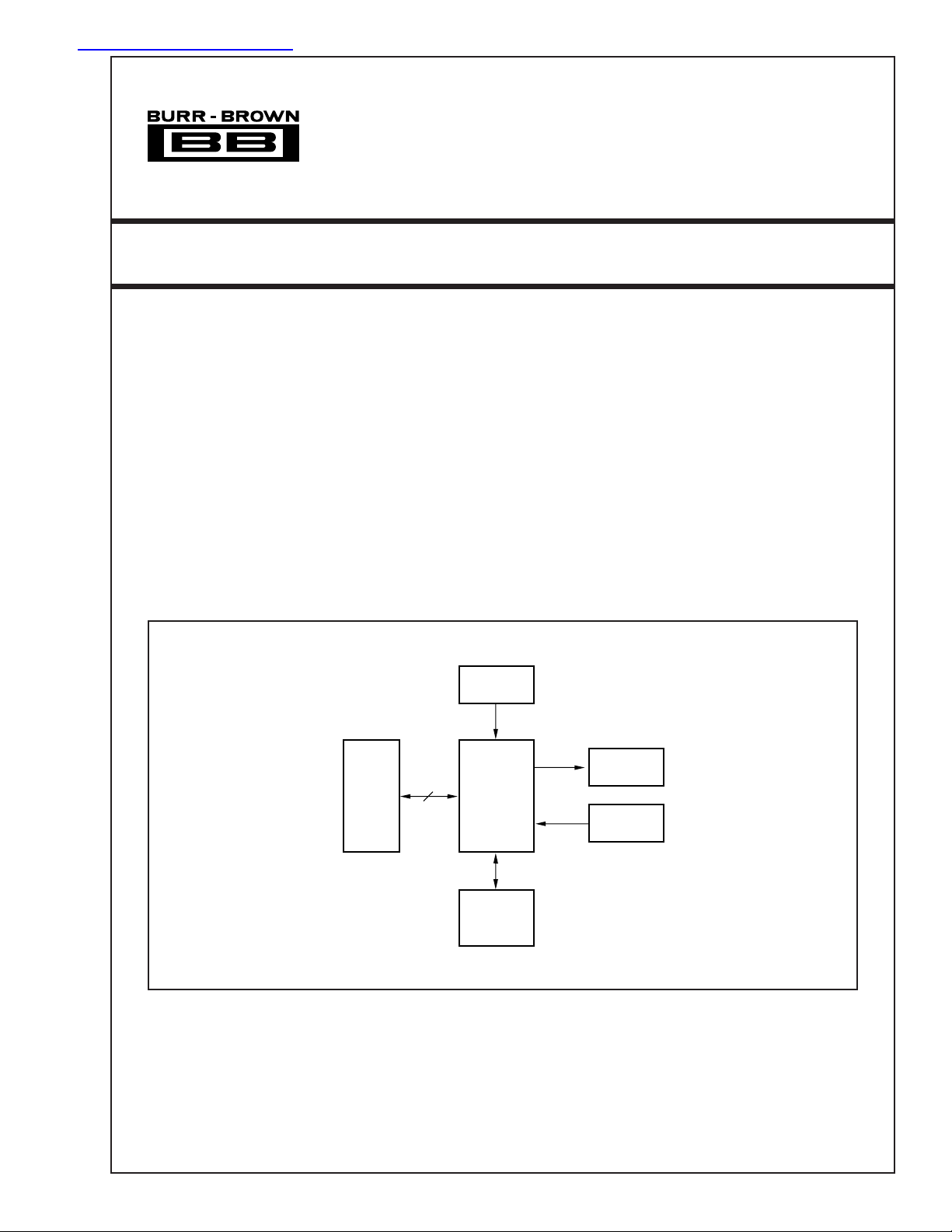
The DEM-PCM3500 is a simple evaluation board for
the PCM3500 single-channel CODEC. It is designed
for quick evaluation of the PCM3500 features and
performance. A prototype area allows for external
analog input and output circuitry to be mounted directly on the evaluation board.
BLOCK DIAGRAM
CMOS 3.3V
or TTL Logic
Digital
Interface
Power Supply
Analog OUT
PCM3500
(DUT)
Analog IN
Mode Control
Switch
SBAU028
International Airport Industrial Park • Mailing Address: PO Box 11400, Tucson, AZ 85734 • Street Address: 6730 S. Tucson Blvd., Tucson, AZ 85706 • Tel: (520) 746-1111
Twx: 910-952-1111 • Internet: http://www.burr-brown.com/ • Cable: BBRCORP • Telex: 066-6491 • FAX: (520) 889-1510 • Immediate Product Info: (800) 548-6132
© 1999 Burr-Brown Corporation LI-536A Printed in U.S.A. August, 1999
Page 2

CONNECTORS
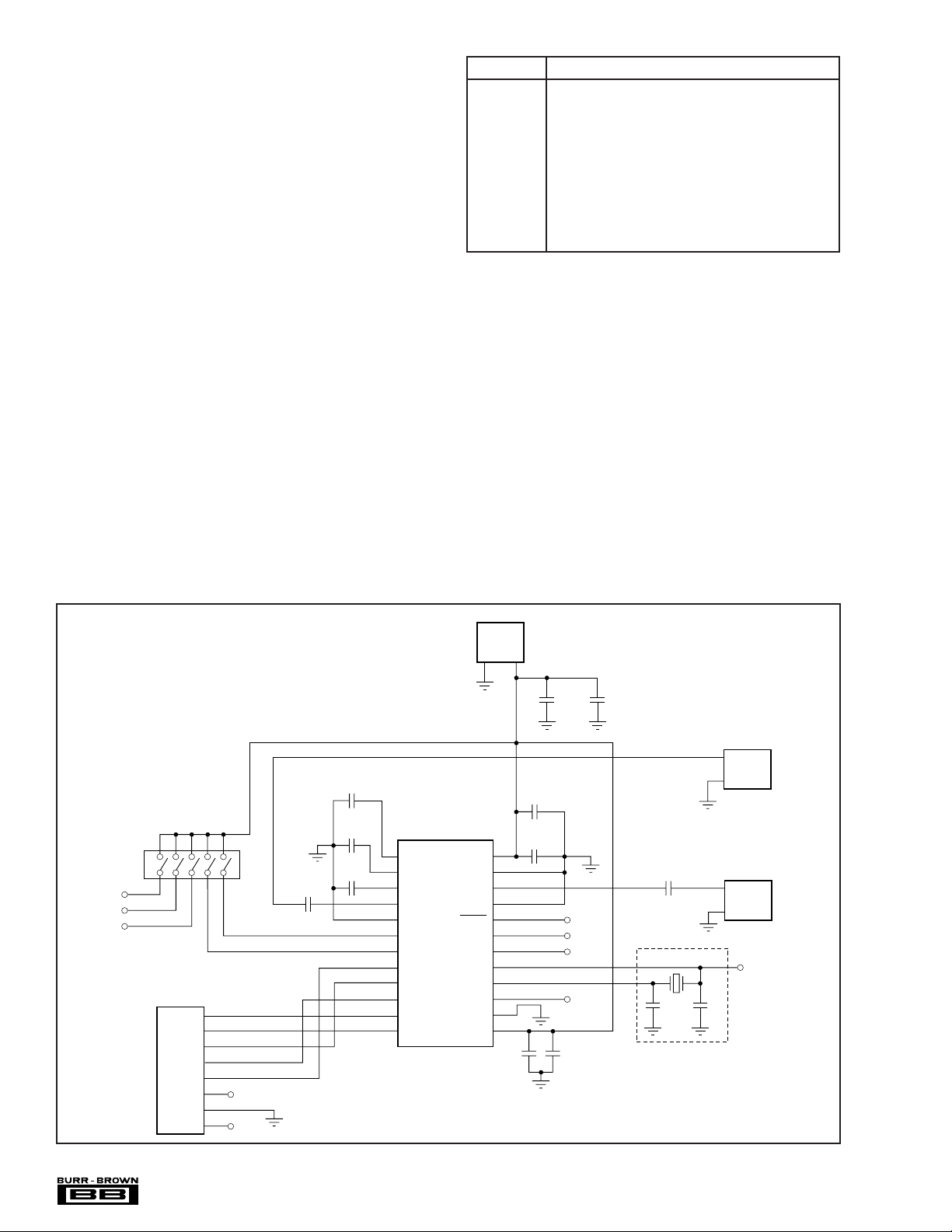
CN1 is the power supply connector for the DEM-PCM3500.
The +VCC pin may be set between +2.7V and +3.6V. The
GND pin should be connected to the negative (–) or ground
terminal of the power supply or battery, and functions as the
analog ground connection.
CN2 is the host interface connector. It includes connections for
the serial interface and system clock input/output. The connector pins correspond directly to the pin names of the PCM3500.
Refer to the PCM3500 data sheet for more details regarding the
operation and requirements for these connections.
CN3 is the analog input connector. The VIN pin is connected
to the PCM3500 analog-to-digital converter input, while the
GND pin is connected to analog ground. The full-scale input
voltage for VIN is 0.6VCC (in Vp-p), or 1.8Vp-p for a +3V
power supply.
CN4 is the analog output connector. The V
nected to the PCM3500 digital-to-analog converter output,
while the GND pin is connected to analog ground. The fullscale output voltage at V
is typically 0.6VCC (in Vp-p),
OUT
or 1.8Vp-p for a +3V power supply.
DIP SWITCH SETTINGS
Table I shows the function of each switch setting for SW1.
Each switch corresponds directly to a pin of the PCM3500.
Refer to the PCM3500 data sheet for more details regarding
the operation and requirements for these pin functions.
pin is con-
OUT
SW1 DESCRIPTION
PWDN H = Power Down Disabled (normal operation)
L = Power Down Enabled
LOOP H = ADC-to-DAC Loop Back Enabled
L = ADC-to-DAC Loop Back Disabled
HPFD H = ADC High Pass Filter Disabled
L = ADC High Pass Filter Enabled
T/S H = Time Slot Mode Enabled
L = Time Slot Mode Disabled
M/S H = Master Mode Enabled
L = Slave Mode Enabled
TABLE I. DIP Switch Settings.
CRYSTAL OSCILLATOR OPERATION
The PCM3500 contains an internal crystal oscillator circuit.
The oscillator can be used to generate the 512fS system clock
(512 times the desired sample frequency). The crystal value
must be equal to 512fS. A fundamental mode, parallel
resonant crystal is recommended. The load capacitors, CS,
should be set in the range from 10pF – 33pF, with 22pF
being the typical value. When using the crystal oscillator,
BCK and FS should be derived from SCKIO when using
Slave mode. Alternatively, the PCM3500 may be set to
Master mode so that the BCK and FS are generated by the
CODEC itself.
DSS105
PWDN
LOOP
HPFD
SW1
DOUT
FSO
DIN
BCK
SCKO
GND
XTI
GND V
CC
CN1
VH2
+
C
C
10
9
C
4.7µF
PDWN
LOOP
HPFD
SCKIO
8
0.1µF
C
11
1µF
+
XTAL
C
S
OPTIONAL
CN3
VH2
V
IN
GND
CN4
VH2
V
OUT
GND
XTI
C
S
100µF
C
2
2.2µF
+
V
COM
V
REF
V
REF
V
IN
AGND
M/S
TSC
BCK
FS
DIN
DOUT
FSO
U1
PCM3500
1
2
V
AGND
V
OUT
AGND
PDWN
LOOP
HPFD
XTI
XTO
SCKIO
DGND
V
CC
DD
C
PWDN
LOOP
HPFD
T/S
M/S
C
1µF
CN2
VH8
FS
SCKIO
XTI
3
4.7µF
+
1
C
4
2
4.7µF
1
+
3
+
4
5
6
7
8
9
10
11
12
24
23
22
21
20
19
18
17
16
15
14
13
C
0.1µF
C
6
0.1µF
C
7
4.7µF
+
+
5
FIGURE 1. Schematic.
®
DEM-PCM3500
2
Page 3

Top Layer
Bottom Layer
FIGURE 2. Printed Circuit Board Plots.
Silk Screen
3
®
DEM-PCM3500
Page 4

IMPORTANT NOTICE
T exas Instruments and its subsidiaries (TI) reserve the right to make changes to their products or to discontinue
any product or service without notice, and advise customers to obtain the latest version of relevant information
to verify, before placing orders, that information being relied on is current and complete. All products are sold
subject to the terms and conditions of sale supplied at the time of order acknowledgment, including those
pertaining to warranty, patent infringement, and limitation of liability.
TI warrants performance of its semiconductor products to the specifications applicable at the time of sale in
accordance with TI’s standard warranty. Testing and other quality control techniques are utilized to the extent
TI deems necessary to support this warranty . Specific testing of all parameters of each device is not necessarily
performed, except those mandated by government requirements.
Customers are responsible for their applications using TI components.
In order to minimize risks associated with the customer’s applications, adequate design and operating
safeguards must be provided by the customer to minimize inherent or procedural hazards.
TI assumes no liability for applications assistance or customer product design. TI does not warrant or represent
that any license, either express or implied, is granted under any patent right, copyright, mask work right, or other
intellectual property right of TI covering or relating to any combination, machine, or process in which such
semiconductor products or services might be or are used. TI’s publication of information regarding any third
party’s products or services does not constitute TI’s approval, warranty or endorsement thereof.
Copyright 2000, Texas Instruments Incorporated
 Loading...