

Page 1

DEM-DAI3793A/3794A EVM
User's Guide
July 2007 AIP Consumer Audio—TI Japan
SBAU127
Page 2

2 SBAU127 – July 2007
Submit Documentation Feedback
Page 3

Contents
Preface ............................................................................................................................... 9
1 Description .............................................................................................................. 11
1.1 Introduction—PCM3793A/94A .................................................................................. 12
1.1.1 Key Features .............................................................................................. 12
1.2 Pin Assignments and Terminal Functions...................................................................... 14
1.3 DEM-DAI3793A/3794A EVM Description ...................................................................... 15
2 Getting Started ......................................................................................................... 17
2.1 Electrostatic Discharge Warning ................................................................................ 18
2.2 Unpacking the EVM ............................................................................................... 18
2.3 Default Configuration ............................................................................................. 19
3 Set-Up Guide ........................................................................................................... 21
3.1 Basic Operating Set-Up .......................................................................................... 22
3.2 Software Control and Operation ................................................................................. 22
3.2.1 User Interface Panel ..................................................................................... 22
3.2.2 Power On/Off Sequence ................................................................................ 23
3.2.3 Module Function Controls ............................................................................... 23
3.2.4 LC89052T (DIR: Digital Audio I/F Receiver) Control Window ...................................... 39
3.2.5 Register Setting History ................................................................................. 40
3.2.6 Register Direct Access .................................................................................. 42
4 Switches and Connectors .......................................................................................... 43
4.1 Overview ............................................................................................................ 44
4.2 Motherboard ....................................................................................................... 44
4.3 Daughter Card #1 (PCM3793A) ................................................................................. 46
4.4 Daughter Card #2 (DIR: LC89052T and DIT: DIT4096) ..................................................... 48
5 Evaluation and Measurements ................................................................................... 49
5.1 Slave Mode With Audio Precision SYS-2722 (Default Setting) ............................................. 50
5.2 Master Mode with Audio Precision SYS-2722 ................................................................. 52
5.3 Combined Master and Slave Modes With PSIA-2722 ........................................................ 54
5.4 Measurements for Dynamic Characteristics ................................................................... 55
5.4.1 Digital-to-Analog (D/A) Performance .................................................................. 56
5.4.2 Analog-to-Digital (A/D) Performance .................................................................. 57
5.4.3 Speaker Output Power Performance .................................................................. 57
5.4.4 Amplitude Versus Frequency Performance ........................................................... 59
5.5 Connection Diagram for Practical Applications ................................................................ 61
5.5.1 Filter Consideration for Speaker Output ............................................................... 62
6 Schematic, PCB Layout, and Bill of Materials ............................................................... 63
6.1 Schematics ......................................................................................................... 64
6.2 Printed Circuit Board Layout ..................................................................................... 66
6.3 Component List .................................................................................................... 71
A Reference .csv Files, Interfacing to DSPs, and Package Information ............................... 73
A.1 Reference .csv Files .............................................................................................. 74
A Related Signal Flow Diagrams ......................................................................... 75
SBAU127 – July 2007 Contents 3
Submit Documentation Feedback
Page 4

A.2 Interfacing to DSPs ............................................................................................... 98
A.2.1 Register Control with DSP Interface ................................................................... 99
A.3 Package Information .............................................................................................. 99
Important Notices ............................................................................................................. 100
4 Contents SBAU127 – July 2007
Submit Documentation Feedback
Page 5

List of Figures
1-1 PCM3793A Pin Assignments ............................................................................................. 14
1-2 PCM3794A Pin Assignments ............................................................................................. 14
1-3 DEM-DAI3793A/3794A EVM System Diagram ......................................................................... 15
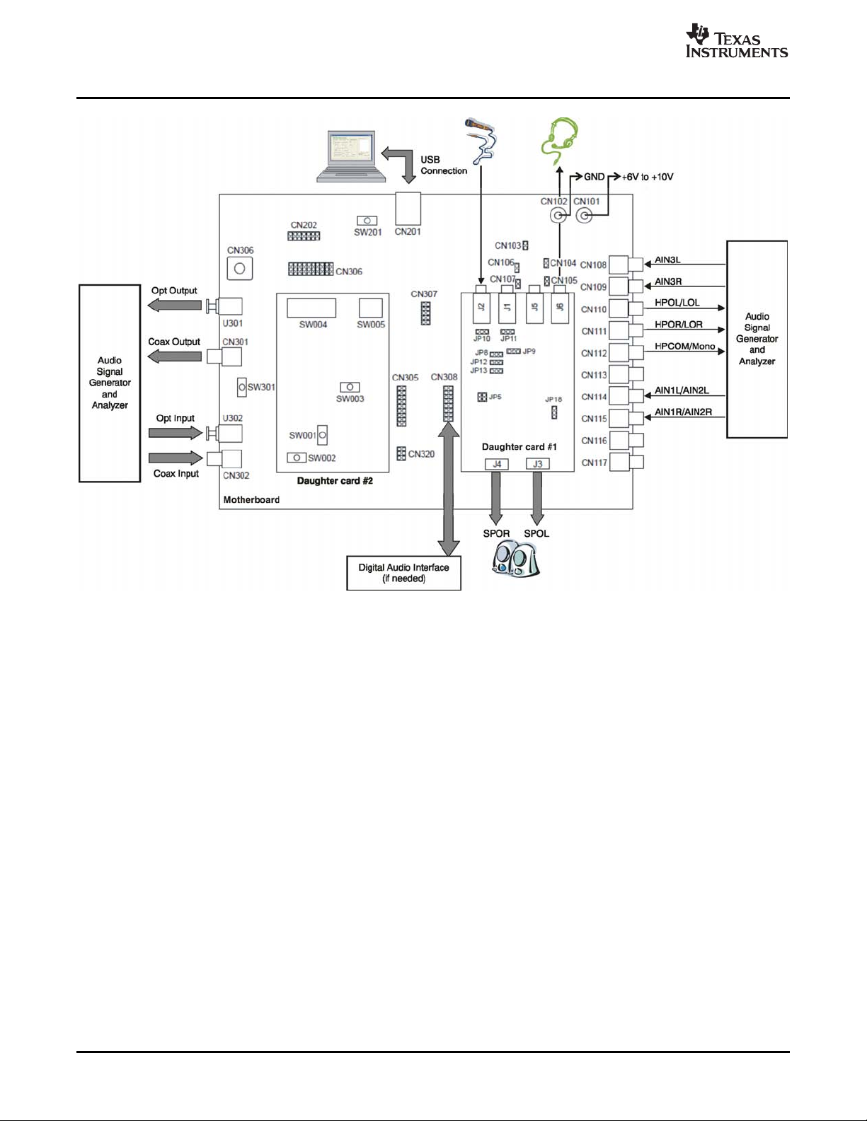
2-1 EVM Configuration ......................................................................................................... 19
2-2 EVM and External Equipment Connections ............................................................................ 20
3-1 User Interface Window .................................................................................................... 22
3-2 Communication Error Message .......................................................................................... 23
3-3 Power On/Off Sequence Function Buttons ............................................................................. 23
3-4 Internal Module Power Up/Down Function Menu Tab ................................................................. 24
3-5 Ramp Up Wave Form with Default Setting ............................................................................. 26
3-6 Ramp Down Wave Form with Default Setting .......................................................................... 26
3-7 Record Function Menu Tab ............................................................................................... 26
3-8 EVM Modules Corresponding to Record Function ..................................................................... 27
3-9 Playback Function Menu Tab ............................................................................................. 28
3-10 Modules Corresponding to Playback Function ......................................................................... 29
3-11 ALC Function Menu Tab .................................................................................................. 30
3-12 ALC Compression and Expansion Characteristics .................................................................... 30
3-13 Signal Processing 1 Function Menu Tab ................................................................................ 31
3-14 Three-Band Tone Control (Bass, Mid, Treble) ......................................................................... 31
3-15 Notch Filter Characteristic Model ........................................................................................ 33
3-16 Example of Measured Notch Filter Characteristic ..................................................................... 33
3-17 Signal Processing 2 Function Menu Tab ................................................................................ 34
3-18 Analog Path Function Menu Tab ......................................................................................... 35
3-19 Modules Corresponding to Analog Path Function ..................................................................... 36
3-20 Audio Interface Function Menu Tab ..................................................................................... 37
3-21 Status Detect Function Menu Tab ....................................................................................... 38
3-22 Digital Amplifier Function Menu Tab ..................................................................................... 39
3-23 LC89052 Interface Format Selection Options .......................................................................... 39
3-24 Register Setting History Window ......................................................................................... 40
3-25 Opening and Modifying a .csv File ....................................................................................... 41
3-26 Register Direct Access Dialog ............................................................................................ 42
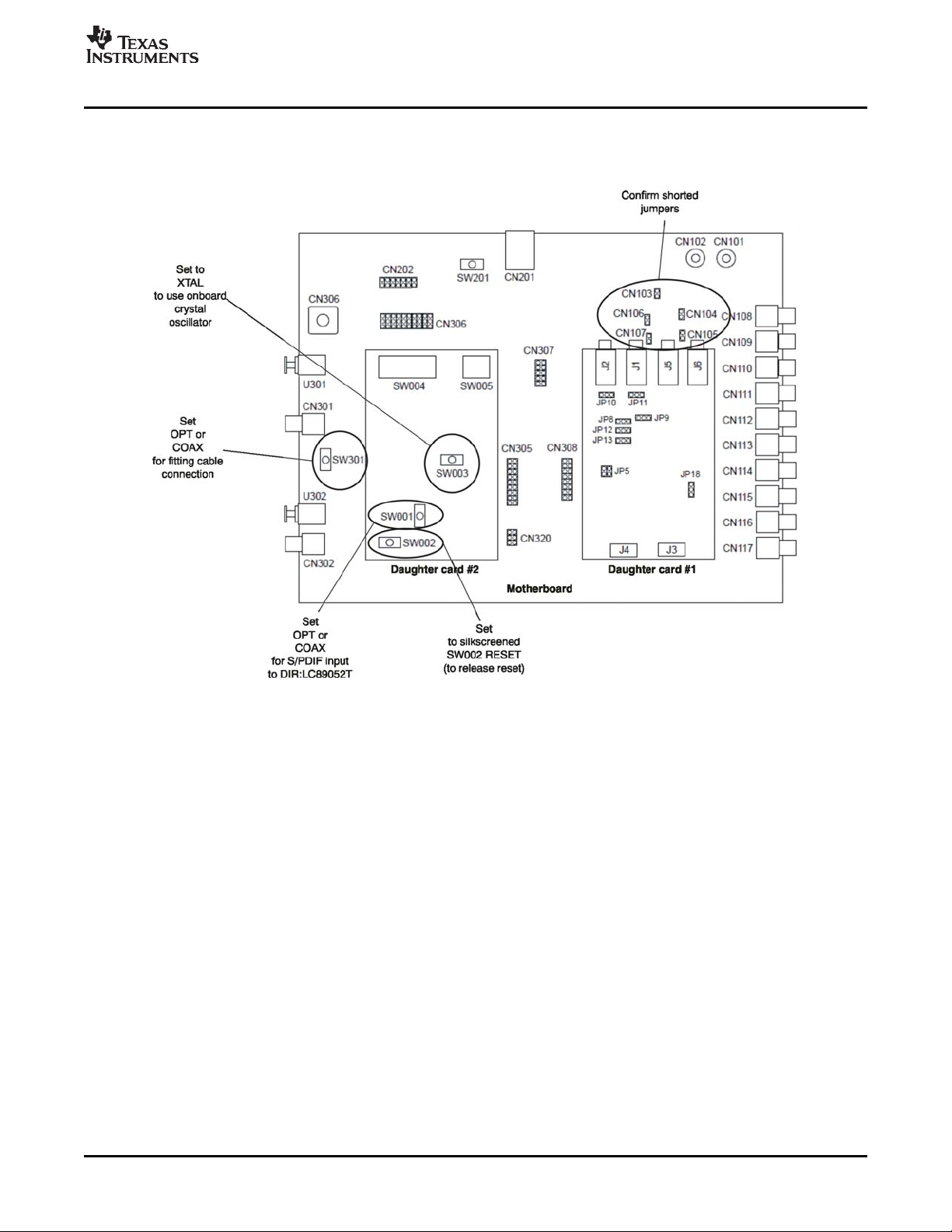
4-1 EVM Configuration ......................................................................................................... 44
4-2 Analog Input Configuration (Daughter Card #1) ........................................................................ 46
4-3 Analog Output Configuration (Daughter Card #1) ..................................................................... 47
5-1 Slave Mode Configuration With SYS-2722 ............................................................................. 50
5-2 Jumper Configuration for Slave Mode (Default) ........................................................................ 51
5-3 Master Mode Configuration With SYS-2722 ............................................................................ 52
5-4 Jumper Configuration for Master Mode ................................................................................. 53
5-5 Combined Master and Slave Mode Configuration with SYS-2722 .................................................. 54
5-6 Jumper Configuration for Combined Master and Slave Modes ...................................................... 55
5-7 Speaker Output Filter Configuration ..................................................................................... 58
5-8 A/D Amplitude vs Frequency Result: BPZ (Zero Data) Input ......................................................... 59
5-9 A/D Amplitude vs Frequency Result: –60dB Input ..................................................................... 59
5-10 A/D Amplitude vs Frequency Result: –1dB Input ...................................................................... 59
5-11 D/A Amplitude vs Frequency Result: BPZ (Zero Data) Input ......................................................... 60
5-12 D/A Amplitude vs Frequency Result: –60dB Input ..................................................................... 60
5-13 D/A Amplitude vs Frequency Result: 0dB Input ........................................................................ 60
5-14 D/A Amplitude vs Frequency Result: Wide Range to 130kHz, BPZ (Zero Data) Input ........................... 60
5-15 Basic Connection Diagram ................................................................................................ 61
5-16 Recommended Ferrite Bead Filter for Speaker Output ............................................................... 62
5-17 Connection for Headphone Output and Insertion Detection .......................................................... 62
6-1 PCM3793A DEM-PCM3793RHB-A Connector (Daughter Card #1) ................................................ 64
SBAU127 – July 2007 List of Figures 5
Submit Documentation Feedback
Page 6

6-2 PCM3793A DEM-PCM3793RHB-A (Daughter Card #1) .............................................................. 65
6-3 PCM3793A DEM-PCM3793RHB-A Board Layout—Silkscreen Side ................................................ 66
6-4 PCM3793A DEM-PCM3793RHB-A Board Layout—Component Side .............................................. 67
6-5 PCM3793A DEM-PCM3793RHB-A Board Layout—Inner Layer 2 .................................................. 68
6-6 PCM3793A DEM-PCM3793RHB-A Board Layout—Inner Layer 3 .................................................. 69
6-7 PCM3793A DEM-PCM3793RHB-A Board Layout—Solder Side .................................................... 70
A-1 Line Output and Headphone Output ..................................................................................... 75
A-2 Headphone Output with Sound Effect ................................................................................... 76
A-3 Cap-Less Headphone Output ............................................................................................. 77
A-4 Headphone Output with Line Input (AIN2L/AIN2R) .................................................................... 78
A-5 Headphone Output with Mono Mic Input (AIN1L, +20dB) ............................................................ 79
A-6 Headphone Output with Mono Diff Mic Input (AIN1L/AIN1R, +20dB) ............................................... 80
A-7 Stereo Speaker Output .................................................................................................... 81
A-8 Mono Speaker Output ..................................................................................................... 82
A-9 Speaker Output with Line Input (AIN2L/AIN2R) ........................................................................ 83
A-10 Speaker Output with Mono Mic Input (AIN1L, +20dB) ................................................................ 84
A-11 Speaker Output with Mono Diff Mic Input (AIN1L/AIN1R, +20dB) ................................................... 85
A-12 Line Input (AIN2L/AIN2R) to Headphone Output ...................................................................... 86
A-13 Mono Line Input (AIN2L) to Headphone Output ....................................................................... 87
A-14 Mono Mic Input (AIN1L, +20dB) to Headphone Output ............................................................... 88
A-15 Mono Diff Mic Input (AIN1L/AIN1R, +20dB) to Headphone Output ................................................. 89
A-16 Mono Mic Input (AIN1L, +20dB) to Speaker Output ................................................................... 90
A-17 Line Input (AIN3L/AIN3R) ................................................................................................. 91
A-18 Mic Input (AIN1L/AIN1R, +20dB)......................................................................................... 92
A-19 Mic Input (AIN1L/AIN1R, +20dB) with ALC ............................................................................. 93
A-20 Mono Mic Input (AIN1L, +20dB) .......................................................................................... 94
A-21 Mono Mic Input (AIN1L, +20dB) with ALC .............................................................................. 95
A-22 Mono Diff Mic Input (AIN1L/AIN1R, +20dB) ............................................................................ 96
A-23 Mono Diff Mic Input (AIN1L/AIN1R, +20dB) with ALC ................................................................ 97
A-24 Slave Mode Operation ..................................................................................................... 98
A-25 Master Mode Operation ................................................................................................... 98
6 List of Figures SBAU127 – July 2007
Submit Documentation Feedback
Page 7

List of Tables
1-1 PCM3793A/94A Terminal Functions ..................................................................................... 14
3-1 Register Mapping for Power Up/Down Module ......................................................................... 24
3-2 PCM3793A/94A Resistor 125(7dh) RES[4:0]: Resistor Value Control .............................................. 25
3-3 PCM3793A/94A Resistor 125(7dh) PMT[1:0]: Power Up/Down Time Control and Register Direct Access ... 25
4-1 Main Power Supply and Regulator ....................................................................................... 44
4-2 Power-Supply Terminals for PCM3793A Power-Supply Pins ....................................................... 44
4-3 Audio I/O .................................................................................................................... 45
4-4 I/F Controller (MSP430 , TUSB3410 ) .................................................................................... 45
4-5 Analog Input and Output—Daughter Card #1 .......................................................................... 46
4-6 Analog Input and Output—Daughter Card #2 .......................................................................... 48
4-7 Audio Clock and Input Data Control Format—Daughter Card #2 .................................................... 48
5-1 D/A Line Output Parameters .............................................................................................. 56
5-2 16 Ω Headphone Output Inserted in Headphone Jack J6 ............................................................. 56
5-3 A/D Line Input Parameters ................................................................................................ 57
5-4 Stereo Speaker Output Parameters ..................................................................................... 57
5-5 Recommended External Parts for Basic Connection Diagram ....................................................... 61
6-1 Bill of Materials ............................................................................................................. 71
A-1 .csv Files .................................................................................................................... 74
A-2 Recommended Power-On Sequence for PCM3793A ................................................................. 99
SBAU127 – July 2007 List of Tables 7
Submit Documentation Feedback
Page 8

SYS-2722, PSIA-2722 are registered trademarks of Audio Precision, Inc.
SPI is a trademark of Motorola, Inc.
I2S, I2C are trademarks of NXP Semiconductors.
TOSLINK is a trademark of Toshiba Corporation.
All other trademarks are the property of their respective owners.
List of Tables8 SBAU127 – July 2007
Submit Documentation Feedback
Page 9

About This Manual
This document provides the information needed to set up and operate the DEM-DAI3793A/3794A EVM
evaluation module, a test platform for the 16-bit, low-power PCM3793A /PCM3794A stereo audio codecs.
For a more detailed description of the PCM3793A/94A products, please refer to the product data sheets
available from the Texas Instruments web site at http://www.ti.com . Support documents are listed in the
sections of this guide entitled Related Documentation from Texas Instruments and Additional
Documentation .
How to Use This Manual
Throughout this document, the abbreviation EVM and the term evaluation module are synonymous with
the DEM-DAI3793A/3794A EVM. The abbreviation PCM3793A/94A refers to the PCM3793A/94A family of
devices. Unless specifically noted, the information presented in this manual applies to both the PCM3793A
and the PCM3794A.
Chapter 1 gives an overview of the PCM3793A/94A family of stereo audio coder/decoder devices
(codecs). The PCM3793A/94A block diagram and primary features are also discussed.
Chapter 2 provides general information regarding EVM handling and unpacking, absolute operating
conditions, and the default switch and jumper configuration. This chapter also discusses the EVM
controller software
Chapter 3 is the hardware setup guide for the EVM, providing all of the necessary information needed to
configure the EVM switches and jumpers for product evaluation.
Chapter 4 reviews the DEM-DAI3793A/3794A EVM switch and jumper configuration.
Chapter 5 discusses how to set up jumpers on the DEM-DAI3793A/3794A EVM motherboard for
performance evaluation using an audio analyzer. It also presents the process for measuring dynamic
characteristics and provides example characteristic data.
Chapter 6 includes the EVM electrical schematics, printed circuit board (PCB) layout, and the bill of
materials.
Preface
SBAU127 – July 2007
Read This First
Information About Cautions and Warnings
This document contains caution statements.
CAUTION
This is an example of a caution statement. A caution statement describes a
situation that could potentially damage your software or equipment.
The information in a caution or a warning is provided for your protection. Please read each caution and
warning carefully.
SBAU127 – July 2007 Read This First 9
Submit Documentation Feedback
Page 10
www.ti.com
Related Documentation From Texas Instruments
Related Documentation From Texas Instruments
The following documents provide information regarding Texas Instruments integrated circuits used in the
assembly of the DEM-DAI3793A/3794A EVM. These documents are available from the TI web site . The
last character of the literature number corresponds to the document revision that is current at the time of
the writing of this User’s Guide. Newer revisions may be available from the TI web site at
http://www.ti.com/ or call the Texas Instruments Literature Response Center at (800) 477–8924 or the
Product Information Center at (972) 644–5580. When ordering, identify the document(s) by both title and
literature number.
Additional Documentation
The following document provides information regarding selected non-TI components that are used in the
assembly of the DEM-DAI3793A/3794A EVM. This document is available from the corresponding
manufacturer.
If You Need Assistance
If you have questions regarding either the use of this evaluation module or the information contained in the
accompanying documentation, please contact the Texas Instruments Product Information Center at (972)
644–5580 or visit the TI web site at www.ti.com .
Data Sheet Literature Number
PCM3793A /PCM3794A Product SLAS529A
data sheet
DIT4096 Product data sheet SBOS225B
Device/Document Manufacturer
LC89052 Sanyo Corporation
FCC Warning
This equipment is intended for use in a laboratory test environment only. It generates, uses, and can
radiate radio frequency energy and has not been tested for compliance with the limits of computing
devices pursuant to subpart J of part 15 of FCC rules, which are designed to provide reasonable
protection against radio frequency interference. Operation of this equipment in other environments may
cause interference with radio communications, in which case the user at his own expense is required to
take whatever measures may be required to correct this interference.
Trademarks
All trademarks are the property of their respective owners.
10 Read This First SBAU127 – July 2007
Submit Documentation Feedback
Page 11
Chapter 1
SBAU127 – July 2007
Description
The DEM-DAI3793A/3794A EVM is a complete evaluation platform for the PCM3793A /PCM3794A 16-bit,
low-power stereo audio codec with microphone bias, headphone, and digital speaker. All necessary
connectors and circuitry are provided for interfacing to audio test systems and commercial audio
equipment.
Topic .................................................................................................. Page
1.1 Introduction—PCM3793A/94A .................................................... 12
1.2 Pin Assignments and Terminal Functions .................................... 14
1.3 DEM-DAI3793A/3794A EVM Description ....................................... 15
SBAU127 – July 2007 Description 11
Submit Documentation Feedback
Page 12

www.ti.com
Introduction—PCM3793A/94A
1.1 Introduction—PCM3793A/94A
1.1.1 Key Features
The PCM3793A/94A is a low-power stereo codec designed for portable digital audio applications. The
device integrates a stereo digital speaker amplifier, headphone amplifier, line amplifier, line input, boost
amplifier, microphone bias, programmable gain control, analog mixing, sound effects, and automatic level
control (ALC) features. (The PCM3794A has no speaker amplifiers.)
It is available in a 5 × 5 QFN package to reduce the overall device footprint. The PCM3793A/94A accepts
Right-Justified, Left-Justified, I2S™, and digital signal processing (DSP) formats, providing an easy
interface to audio DSPs, as well as decoders and encoder chips. Sampling rates up to 50kHz are
supported. The user-programmable functions are accessible through a two- or three-wire serial control
port.
Major features of the PCM3793A/94A include:
• Analog Front End:
– Stereo single-ended input with multiplexer (mux)
– Mono differential input
– Stereo programmable gain amplifier (PGA)
– Microphone amplifier (20dB) and bias
• Analog Back End:
– Stereo/Mono line output with volume
– Stereo/Mono headphone amplifier with volume and capless mode
– Stereo/Mono digital speaker amplifier (BTL) with volume
• Analog Performance:
– Dynamic range: 93dB (digital-to-audio converter [DAC])
– Dynamic range: 90dB (analog-to-digital converter [ADC])
– 40mW + 40mW headphone output at R
– 700mW + 700mW speaker output at R
= 16 Ω
L
= 8 Ω
L
• Power Supply Voltage
– 1.71V to 3.6V for digital I/O section
– 1.71V to 3.6V for digital core section
– 2.4V to 3.6V for analog section
– 2.4V to 3.6V for power amplifier section
• Low Power Dissipation:
– 7mW in playback, 1.8V/2.4V, 48kHz
– 13mW in record, 1.8V/2.4V, 48kHz
– 3.3 μ W in power-down
• Sampling Frequency: 5kHz to 50kHz
• Automatic Level Control for Recording
• Operation From a Single Clock Input without PLL
• System Clock:
– Common-audio clock (256f
/384f
S
), 12MHz/24MHz, 13MHz/26MHz, 13.5MHz/27MHz,
S
19.2MHz/38.4MHz, 19.68MHz/39.36MHz
• Headphone Plug Insert Detection
• I2C™ or SPI™ Serial Control
12 Description SBAU127 – July 2007
Submit Documentation Feedback
Page 13

www.ti.com
blank
• Programmable Function by Register Control:
– Digital attenuation of DAC: 0dB to –62dB
– Digital gain of DAC: 0dB, 6dB, 12dB, 18dB
– Power up/down control for each module
– 6dB to –70dB gain for analog outputs
– 30dB to –12dB gain for analog inputs
– 0dB/20dB selectable for microphone input
– 0dB to –21dB gain for analog mixing
– Parameter settings for ALC
– Three-band tone control and 3D sound
– High-pass filter: 4Hz, 120Hz, 240Hz
– Two-stage programmable notch filter
– Analog mixing control
• Pop-Noise Reduction Circuit
• Short and Thermal Protection Circuit
• Package: 5mm × 5mm QFN Package
• Operating Temperature Range: –40 ° C to +85 ° C
Introduction—PCM3793A/94A
SBAU127 – July 2007 Description 13
Submit Documentation Feedback
Page 14
www.ti.com
HPOR/LORAIN2L
BCK
AIN2R
24123222321420519618717
8
16
25
15
26
14
27
13
28
12
29
1130
1031
932
SPOLP
AIN3L
SPOLN
AIN3R
PGND
MICB
V
PA
V
C
C
SPORP
AGND
SPORN
V
COM
HPCOM/MONO
HPOL/LOL
PCM3793ARHB
(TOPVIEW)
AIN1R
DIN
AIN1L
DOUT
MODE
V
IO
MS/ADR
V
DD
MD/SDA
DGND
MC/SCL
SCKI
LRCK
HDTI
HPOR/LORAIN2L
BCK
AIN2R
24123222321420519618717
8
16
25
15
26
14
27
13
28
12
29
1130
1031
932
NC
AIN3LNCAIN3R
PGND
MICB
V
PA
V
C
C
NC
AGNDNCV
COM
HPCOM/MONO
HPOL/LOL
PCM3794ARHB
(TOPVIEW)
AIN1R
DIN
AIN1L
DOUT
MODE
V
IO
MS/ADR
V
DD
MD/SDA
DGND
MC/SCL
SCKI
LRCK
HDTI
Pin Assignments and Terminal Functions
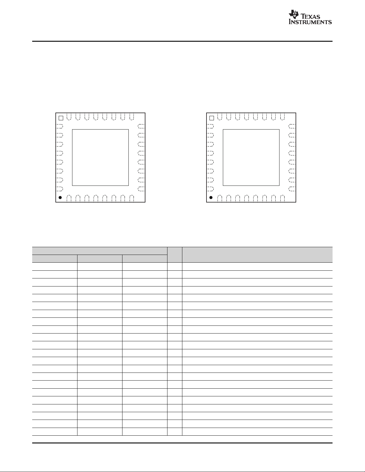
1.2 Pin Assignments and Terminal Functions
Figure 1-1 and Figure 1-2 show the pin assignments for the PCM3793A/94A. Table 1-1 lists the terminal
functions.
Figure 1-1. PCM3793A Pin Assignments Figure 1-2. PCM3794A Pin Assignments
Table 1-1. PCM3793A/94A Terminal Functions
TERMINAL
NAME PCM3793ARHB PCM3794ARHB I/O DESCRIPTION
AGND 19 19 – Ground for analog
AIN1L 27 27 I Analog input 1 for L-channel
AIN1R 26 26 I Analog input 1 for R-channel
AIN2L 25 25 I Analog input 2 for L-channel
AIN2R 24 24 I Analog input 2 for R-channel
AIN3L 23 23 I Analog input 3 for L-channel
AIN3R 22 22 I Analog input 3 for R-channel
BCK 1 1 I/O Serial bit clock
DGND 6 6 – Digital ground
DIN 2 2 I Serial audio data input
DOUT 3 3 O Serial audio data output
HDTI 8 8 I Headphone plug insertion detection
HPCOM/MONO 9 9 O Headphone common/mono line output
HPOL/LOL 17 17 O Headphone/lineout for R-channel
HPOR/LOR 16 16 O Headphone/lineout for L-channel
LRCK 32 32 I/O Left and right channel clock
MC/SCL 31 31 I Mode control clock for three-wire/two-wire interface
MD/SDA 30 30 I/O Mode control data for three-wire/two-wire interface
MICB 21 21 O Microphone bias source output
MODE 28 28 I Two- or three-wire interface selection (low: SPI; high: I2C)
MS/ADR 29 29 I Mode control select for three-wire/two-wire interface
PGND 13 13 – Ground for speaker power amplifier
14 Description SBAU127 – July 2007
Submit Documentation Feedback
Page 15
www.ti.com
DEM-DAI3793A/3794A EVM Description
Table 1-1. PCM3793A/94A Terminal Functions (continued)
TERMINAL
NAME PCM3793ARHB PCM3794ARHB I/O DESCRIPTION
SCKI 7 7 I System clock
SPOLN 14 – O Speaker output L-channel for negative (PCM3793A only)
SPOLP 15 – O Speaker output L-channel for positive (PCM3793A only)
SPORN 10 – O Speaker output R-channel for negative (PCM3793A only)
SPORP 11 – O Speaker output R-channel for positive (PCM3793A only)
V
CC
V
COM
V
DD
V
IO
V
PA
20 20 – Analog power supply
18 18 – Analog common voltage
5 5 – Power supply for digital core
4 4 – Power supply for digital I/O
12 12 – Power supply for power amplifier
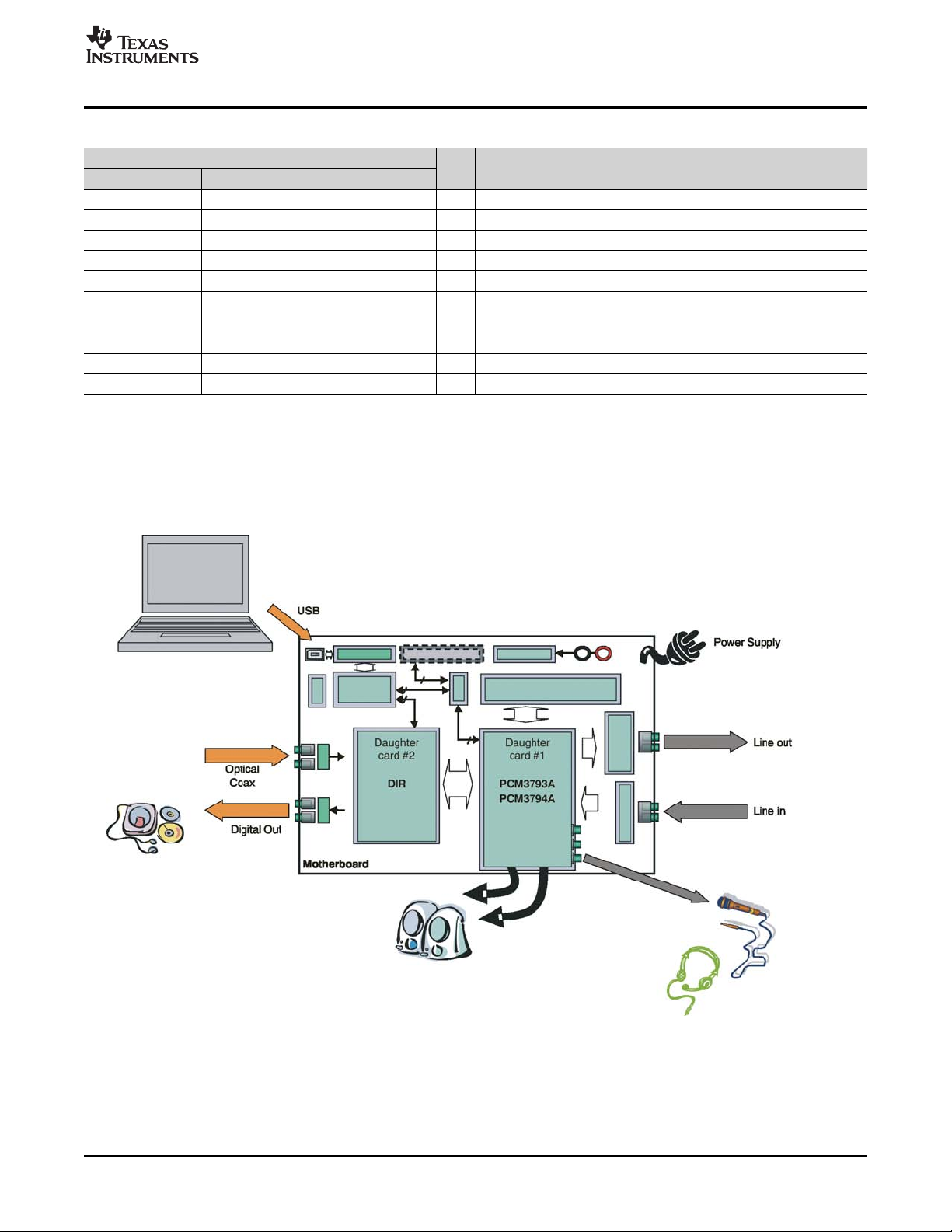
1.3 DEM-DAI3793A/3794A EVM Description
The DEM-DAI3793A/3794A evaluation module permits user control of the entire PCM3793A/94A system.
The EVM allows users to test playback with and without digital input; recording through digital input/output
with an optical cable or RCA jacks; a line input/output; stereo speaker output (PCM3793A only);
stereo/mono headphone output; and stereo/mono microphone input, as shown in Figure 1-3 .
Figure 1-3. DEM-DAI3793A/3794A EVM System Diagram
SBAU127 – July 2007 Description 15
Submit Documentation Feedback
Page 16

Description 16 SBAU127 – July 2007
Submit Documentation Feedback
Page 17
Getting Started
This chapter provides information regarding DEM-DAI3793A/3794A EVM handling and unpacking,
absolute operating conditions, and a description of the factory default switch and jumper configuration.
Topic .................................................................................................. Page
2.1 Electrostatic Discharge Warning ................................................. 18
2.2 Unpacking the EVM ................................................................... 18
2.3 Default Configuration ................................................................ 19
Chapter 2
SBAU127 – July 2007
SBAU127 – July 2007 Getting Started 17
Submit Documentation Feedback
Page 18

www.ti.com
Electrostatic Discharge Warning
2.1 Electrostatic Discharge Warning
Many of the components on the DEM-DAI3793A/3794A EVM are susceptible to damage by electrostatic
discharge (ESD). Customers are advised to observe proper ESD handling precautions when unpacking
and handling the EVM, including the use of a grounded wrist strap at an approved ESD workstation.
Failure to observe ESD handling procedures may result in damage to EVM
components.
2.2 Unpacking the EVM
Upon opening the DEM-DAI3793A/3794A EVM package, please check to make sure that the following
items are included:
• One DEM-DAI/LPC-USB (Motherboard )
• One DEM-PCM3793RHB-A (Daughter Card #1 )
• One DEM-TRCV/LPC (Daughter Card #2 )
If any of these items are missing, please contact the Texas Instruments Product Information Center
nearest you to inquire about a replacement.
CAUTION
Getting Started18 SBAU127 – July 2007
Submit Documentation Feedback
Page 19
www.ti.com
Default Configuration
2.3 Default Configuration
Figure 2-1 and Figure 2-2 illustrate the default EVM configuration and the default external equipment
connection configuration, respectively.
Figure 2-1. EVM Configuration
SBAU127 – July 2007 Getting Started 19
Submit Documentation Feedback
Page 20
www.ti.com
Default Configuration
Figure 2-2. EVM and External Equipment Connections
The factory default configuration for the DEM-DAI3793A/3794A EVM is listed below.
Motherboard:
• CN101, CN102: Connect dc power supply positive lead (+) to CN101 and negative lead (–) to CN102
• SW301: Set Opt or Coax output for the proper cable connection
Daughter Card #1 (DEM-PCM3793RHB-A):
• JP14, JP15, JP16, JP17, and JP19: these jumper pins should not be used
• For other jumper settings, please refer to the chapter, Switches and Connectors.
Daughter Card #2 (DEM-TRVC/LPC):
• SW001: Set Opt or Coax for S/PDIF input to DIR:LC89052T
• SW002: Set to silkscreen SW002 RESET side (releasing reset)
• SW003: Set X’tal to use onboard crystal oscillator
There is no need to change the setting of the shorting plugs for basic operation. Jumper settings strongly
depend on the audio interface.
20 Getting Started SBAU127 – July 2007
Submit Documentation Feedback
Page 21
Set-Up Guide
This chapter discusses how to set up the DEM-DAI3793A/3794A EVM and describes the EVM software.
Topic .................................................................................................. Page
3.1 Basic Operating Set-Up ............................................................. 22
3.2 Software Control and Operation .................................................. 22
Chapter 3
SBAU127 – July 2007
SBAU127 – July 2007 Set-Up Guide 21
Submit Documentation Feedback
Page 22
www.ti.com
Basic Operating Set-Up
3.1 Basic Operating Set-Up
Follow these steps to set up the DEM-DAI3793A/3794A EVM for operation.
Step 1. When using the kit for the first time, install the TUSB3410 VCP (Virtual COM Port) driver to
Step 2. Connect the audio signal sources and/or receiver, using one of these connections:
• S/PDIF cable (optical or coaxial)
• Analog input/output (RCA)
Step 3. Connect microphone, speakers, headphone, an audio amplifier, or measurement equipment,
Step 4. Confirm that jumpers CN103–CN107 are shorted.
Step 5. Connect the USB cable between the host PC and the motherboard (CN201).
Step 6. Apply +6V to +10V to the motherboard (CN101, CN102 for power supply).
Step 7. Execute EVM3793A.exe.
When the installation is complete, the EVM software is ready to use.
3.2 Software Control and Operation
This section of the user's guide reviews the operation and configuration of the EVM controller software.
the host PC. To install the driver, refer to the Virtual COM Port Driver Installation
Instructions.pdf located in the DEM-DAI3793 folder of the software CD or available through
the TI web site .
if necessary.
3.2.1 User Interface Panel
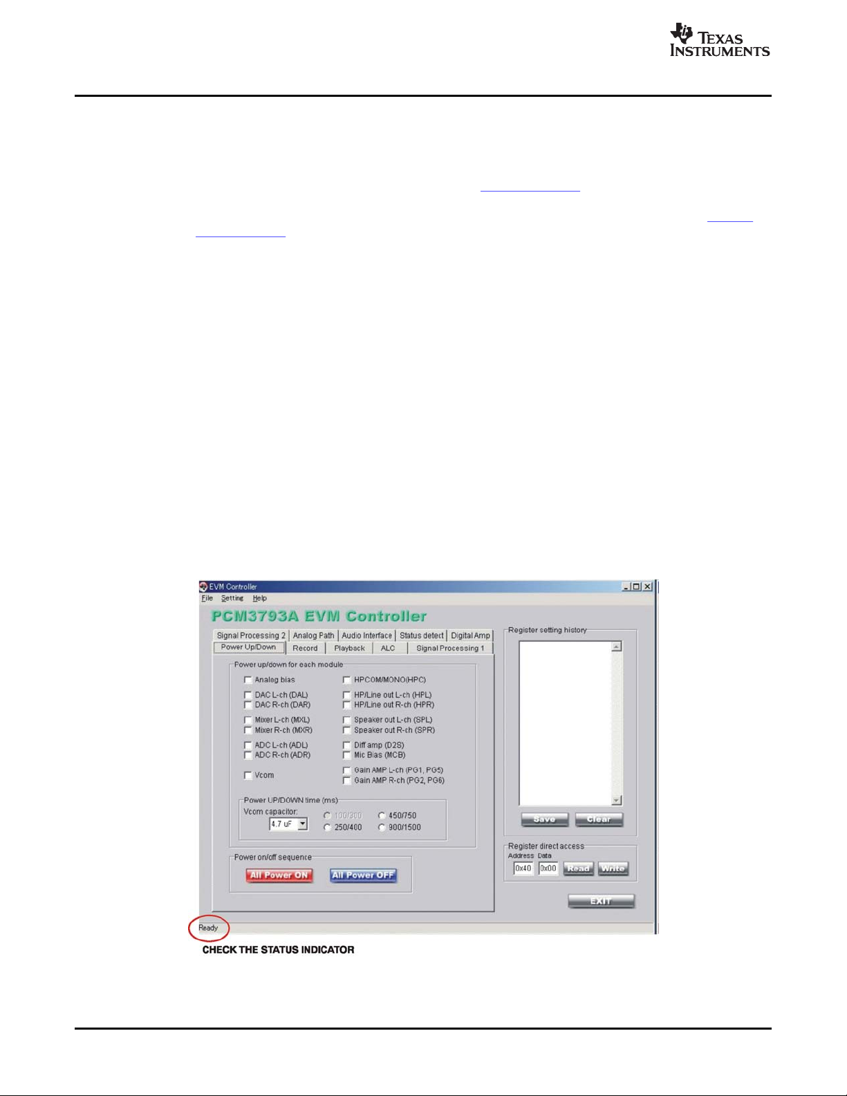
After finishing the installation process (as explained in Section 3.1 ), the user interface panel shown in
Figure 3-1 appears.
Figure 3-1. User Interface Window
22 Set-Up Guide SBAU127 – July 2007
Submit Documentation Feedback
Page 23
www.ti.com
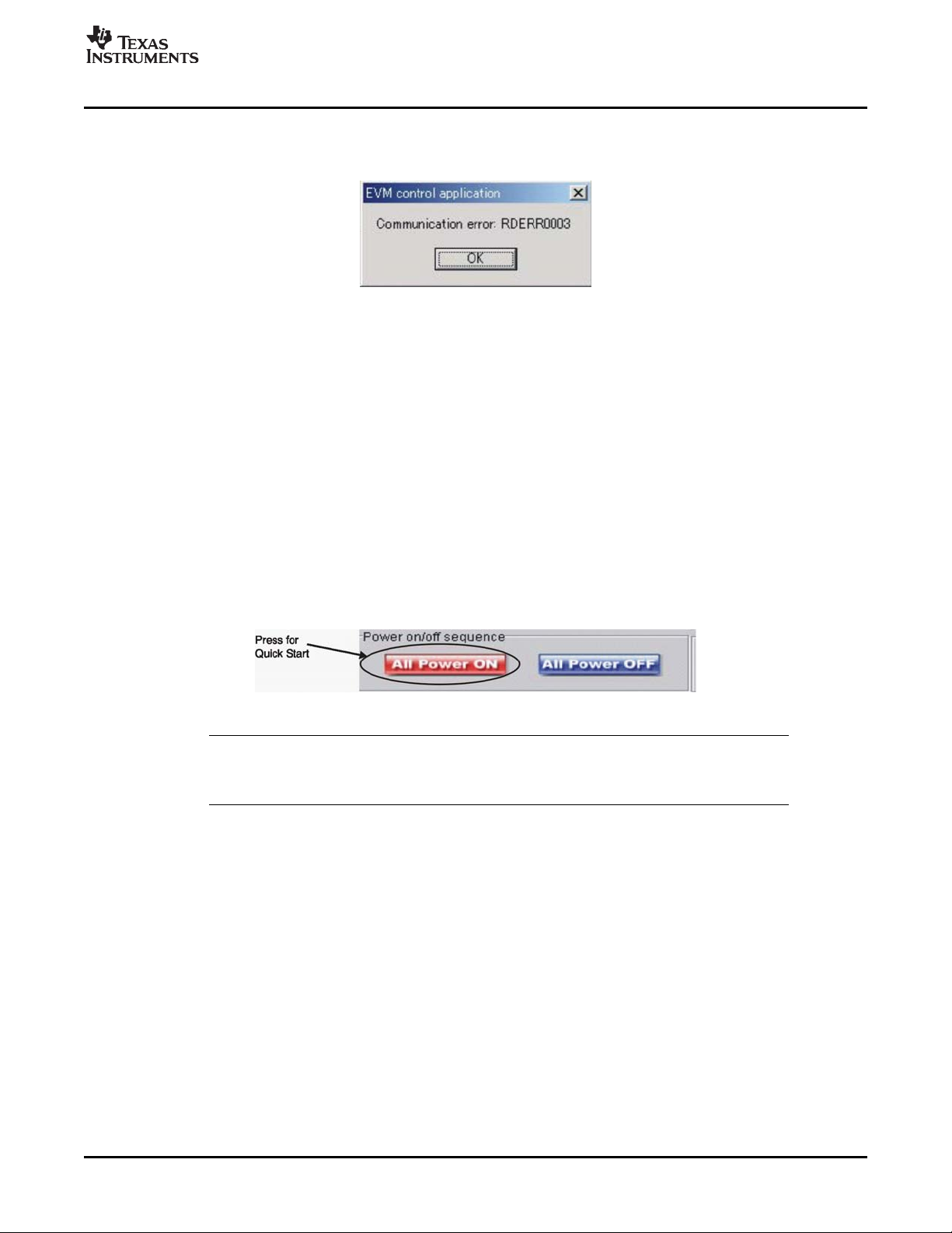
Check to see that a Ready notation appears in the lower left-hand corner after successful I2C
communication is established. Otherwise, you will see an error box showing a communication error (as
shown in Figure 3-2 ).
If you received this message, confirm the set-up procedures and restart the software. Shut it down and
then execute EVM3793A.exe.
There are four primary sections of the user interface panel (see Figure 3-1 ):
• Module controller, for functions such as playback, signal processing, audio format, and so forth;
• Power on/off sequence controller
• Register setting history controller
• Register direct access controller
3.2.2 Power On/Off Sequence
By default, each module is set without any of the checkboxes toggled in the Power Up/Down menu. All
modules are set to a power-down condition.
Click All Power On (the red box, as shown in Figure 3-3 ) to easily start EVM operation, instead of
powering up the module manually.
Software Control and Operation
Figure 3-2. Communication Error Message
Note: If pressing the Power On/Off sequence button has no effect, check to see that the two
3.2.3 Module Function Controls
The DEM-DAI3793A/3794A EVM controller software contains 10 tabs:
• Power Up/Down: to power up and power down each module
• Record: executes gain control for ADC input
• Playback: executes headphone/speaker gain control and digital ATT
• ALC: tunes the Automatic Level Control function
• Signal Processing 1: adjusts the tone control and notch filter coefficient
• Signal Processing 2: controls DAC oversampling, de-emphasis, and high-pass filtering
• Analog Path: selects analog input, differential input, and analog mixer
• Audio Interface: selects the audio interface for ADC and DAC
• Status Detect: controls headphone short detection and speaker thermal protection
• Digital Amp: tune switching frequency for digital amplifier
This section discusses each of these tab operations and controls.
Figure 3-3. Power On/Off Sequence Function Buttons
files power_on.csv and power_off.csv are located in the same folder on the PC as the
EVM software (EVM3793A.exe).
SBAU127 – July 2007 Set-Up Guide 23
Submit Documentation Feedback
Page 24
www.ti.com
Software Control and Operation
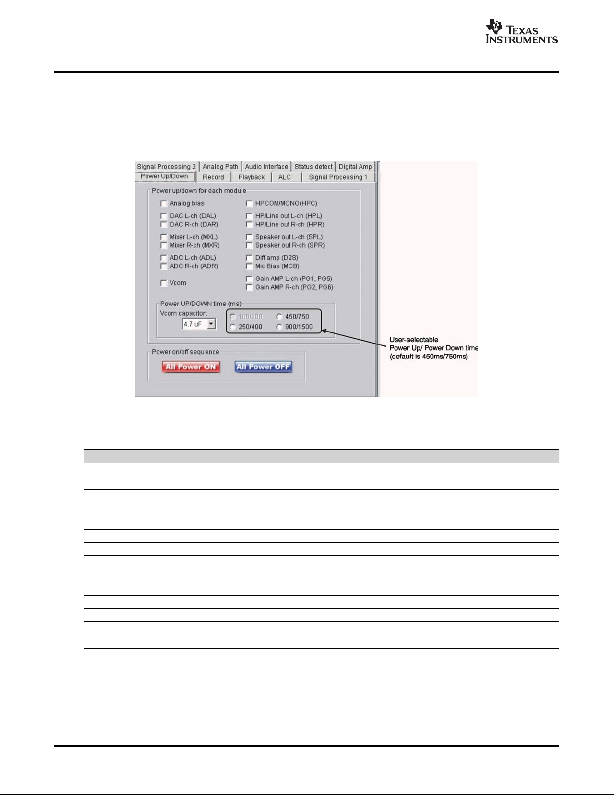
3.2.3.1 Power Up/Down
This menu (shown in Figure 3-4 ) allows users to manually power up or power down each module. Click
the appropriate checkboxes to power up or power down a specific module. Table 3-1 shows the register
mapping for each module setting.
Abbreviations such as DAL/DAR, MXL/MXR, and ADL/ADR stand for corresponding modules that are
described in the block diagram of the PCM3793A (see Figure 3-8 ).
Figure 3-4. Internal Module Power Up/Down Function Menu Tab
Table 3-1. Register Mapping for Power Up/Down Module
Check Box Internal Module Register
Analog Bias Analog bias Reg#73 bit7 [PBIS]
Vcom Analog common voltage Reg#74 bit0 [PCOM]
HP COM/MONO (HPC) Headphone common/mono-out buffer Reg#73 bit4 [PHPC]
Mixer L-ch (XML) Analog mixer L-ch Reg#72 bit0 [PMXL]
Mixer R-ch (XMR) Analog mixer R-ch Reg#72 bit1 [PMXR]
HP/Line out L-ch (HPL) Headphone / Line out amp L-ch Reg#73 bit2 [PHPL]
HP/Line out R-ch (HPR) Headphone / Line out amp R-ch Reg#73 bit3 [PHPR]
DAC L-ch (DAL) DAC and interpolation filter L-ch Reg#73 bit5 [PDAL]
DAC R-ch (DAR) DAC and interpolation filter R-ch Reg#73 bit6 [PDAR]
Speaker out L-ch (SPL) Speaker amp L-ch Reg#73 bit0 [PSPL]
Speaker out R-ch (SPR) Speaker amp R-ch Reg#73 bit1 [PSPR]
ADC L-ch (ADL) ADC and decimation filter L-ch Reg#82 bit0 [PADL]
ADC R-ch (ADR) ADC and decimation filter R-ch Reg#82 bit1 [PADR]
Gain AMP L-ch (PG1, PG5) Gain amp L-ch (PG1 and PG5) Reg#82 bit4 [PAIL]
Gain AMP R-ch (PG2, PG6) Gain amp R-ch (PG2 and PG6) Reg#82 bit5 [PAIR]
Diff amp (D2S) D2S for AIN1 Reg#82 bit3 [PADS]
Mic Bias (MCB) Mic bias amp Reg#82 bit2 [PMCB]
Set-Up Guide24 SBAU127 – July 2007
Submit Documentation Feedback
Page 25
www.ti.com
Power Up/Down Time (ms) Options
It is possible to select the V
vice-versa by choosing a V
4.7 μ F V
The 4.7 μ F V
recommended power-on sequence discussed in the product data sheet .
To select a different V
Be sure to change the capacitor on the EVM to the same value (1.0 μ F, 2.2 μ F or 10 μ F).
The combination of PTM[1:0] and RES[4:0] determines the V
Table 3-2 and Table 3-3 .
To set the ramp up or down time without directly accessing the registers, users can select a V
capacitor value and time in the group box. The ramp up waveform with the default setting is shown in
Figure 3-5 , and the ramp down waveform in Figure 3-6 , as references.
capacitor is chosen as the default setting (this capacitor is also mounted on the EVM).
COM
COM
Power Up/Down Time (ms) Options
ramp up/down time from GND level to a common voltage level or
COM
capacitor value and time by choosing one of the available checkboxes. A
COM
capacitor is the recommended value for operating the EVM. This configuration is the
value, choose the appropriate value from the V
COM
ramp up/down time, as described in
COM
capacitor drop-down menu.
COM
Table 3-2. PCM3793A/94A Resistor 125(7dh)
RES[4:0]: Resistor Value Control
RES [4:0] V
10000 60 k Ω
11000 24 k Ω
11100 12 k Ω
11110 6 k Ω
Others Reserved
Resistor Value
COM
COM
Table 3-3. PCM3793A/94A Resistor 125(7dh) PMT[1:0]: Power Up/Down Time Control and
Register Direct Access
V
Capacitor Power-Up Time Power-Down Time Register Direct
COM
[ μ F] RES[4:0] PTM[1:0] [ms] [ms] Access
10 11110 00 450 750 0x7D1E
11100 11 900 1500 0x7D7C
11000 Do not set — — —
10000 Do not set — — —
4.7 11110 01 250 400 0x7D3E
11100 00 450 750 0x7D1C (default)
11000 11 900 1500 0x7D78
10000 Do not set — — —
2.2 11110 10 100 300 0x7D5E
11100 01 250 400 0x7D3C
11000 00 450 750 0x7D18
10000 11 900 1500 0x7D70
1.0 11110 Do not set — — —
11100 10 100 300 0x7D5C
11000 01 250 400 0x7D38
10000 00 450 750 0x7D10
SBAU127 – July 2007 Set-Up Guide 25
Submit Documentation Feedback
Page 26
www.ti.com
Power Up/Down Time (ms) Options
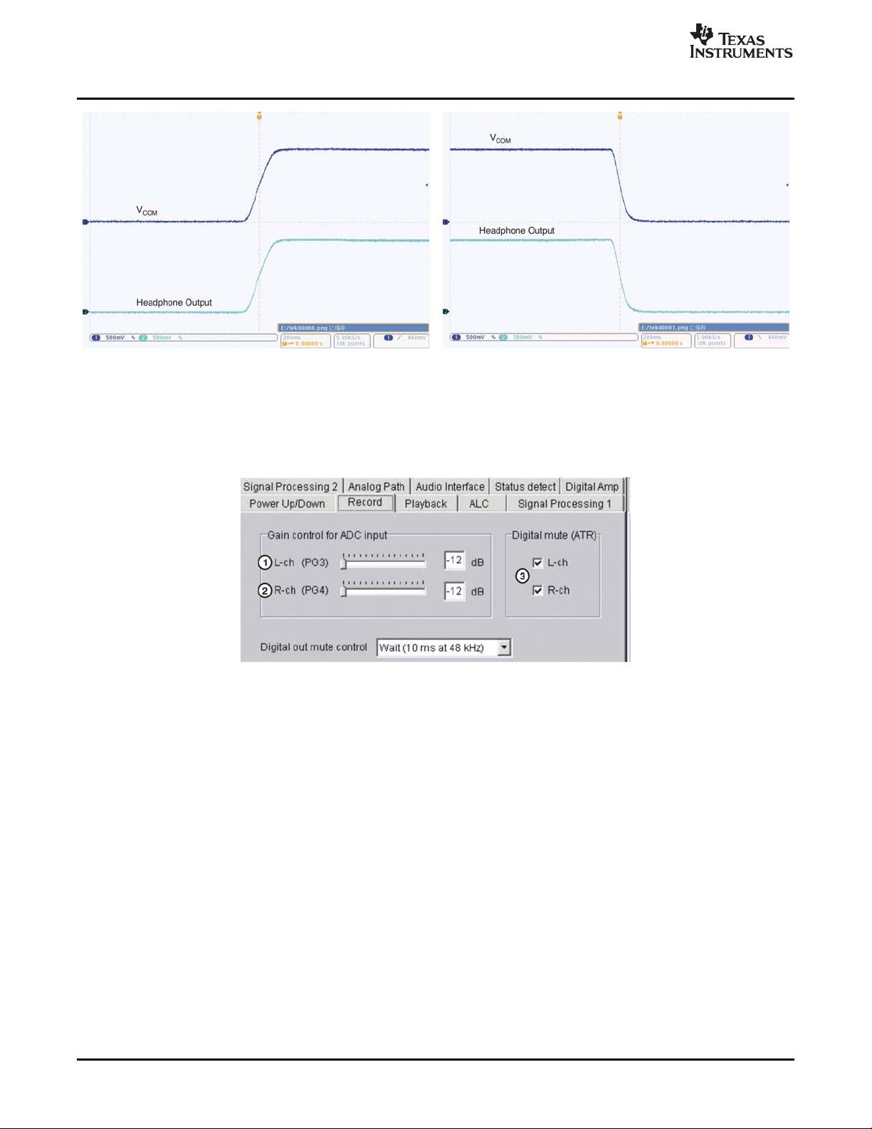
Figure 3-5. Ramp Up Wave Form with Default Figure 3-6. Ramp Down Wave Form with
3.2.3.2 Record
Figure 3-7 shows the Record function tab options.
Setting Default Setting
Figure 3-7. Record Function Menu Tab
26 Set-Up Guide SBAU127 – July 2007
Submit Documentation Feedback
Page 27
www.ti.com
V
COM
AIN3L
AIN2L
AIN1L
AIN2R
AIN3R
AIN1R
MICB
DS
ADC
BCK
DIN
DOUT LRCK
MS/
ADR
MC/
SCL
MD/
SDA
MODE
SerialInterface(SPI/I C)
2
SCKI
AudioInterface
V
PA
PGND VCCAGND
V
DD
DGND
HPOL/
LOL
HPOR/
LOR
SPOLP
SPOLN
SPORP
SPORN
HDTI
MUX1
DAL
ADL
DAR
HPCOM/
MONO
COM
HPR
HPL
HPC
LOUT
ROUT
+30dBto
12dB-
+30dBto
12dB-
PG5
V
IO
MONO
MCB
COM
PG1
PG3
PG4
MONO
ADR
D2S
MUX3
MUX2
MUX4
0dBto
21dB-
0dBto
21dB-
PG6
PG2
0dB/
+20dB
0dB/
+20dB
Digital
Filter
Digital
Filter
Digital
Filter
Digital
Filter
MXL
MXR
HPOR
HPOL
COM
V
COM
ATP
(0dBto 62dB,Mute)-
DGC
(0dB/+6dB/+12dB/+18dB)
SilentPopNoise
Controller
ModuleofPossiblePowerUp/Down
PCM3794AhasnoSpeakerOutput
SW1
SW2
SW3
SW6
SW5
SW4
V
COM
PowerOn
Reset
Power
Up/Down
Manager
Clock
Manager
AnalogInputR-Channel
AnalogInputL-Channel
ATR
(Mute)
DS
ADC
DS
DAC
DS
DAC
+
+
+
+6dBto
70dB-
+6dBto
70dB-
+6dBto 70dB-
+6dBto 70dB-
SPL
SPR
1
2
3
MicBias
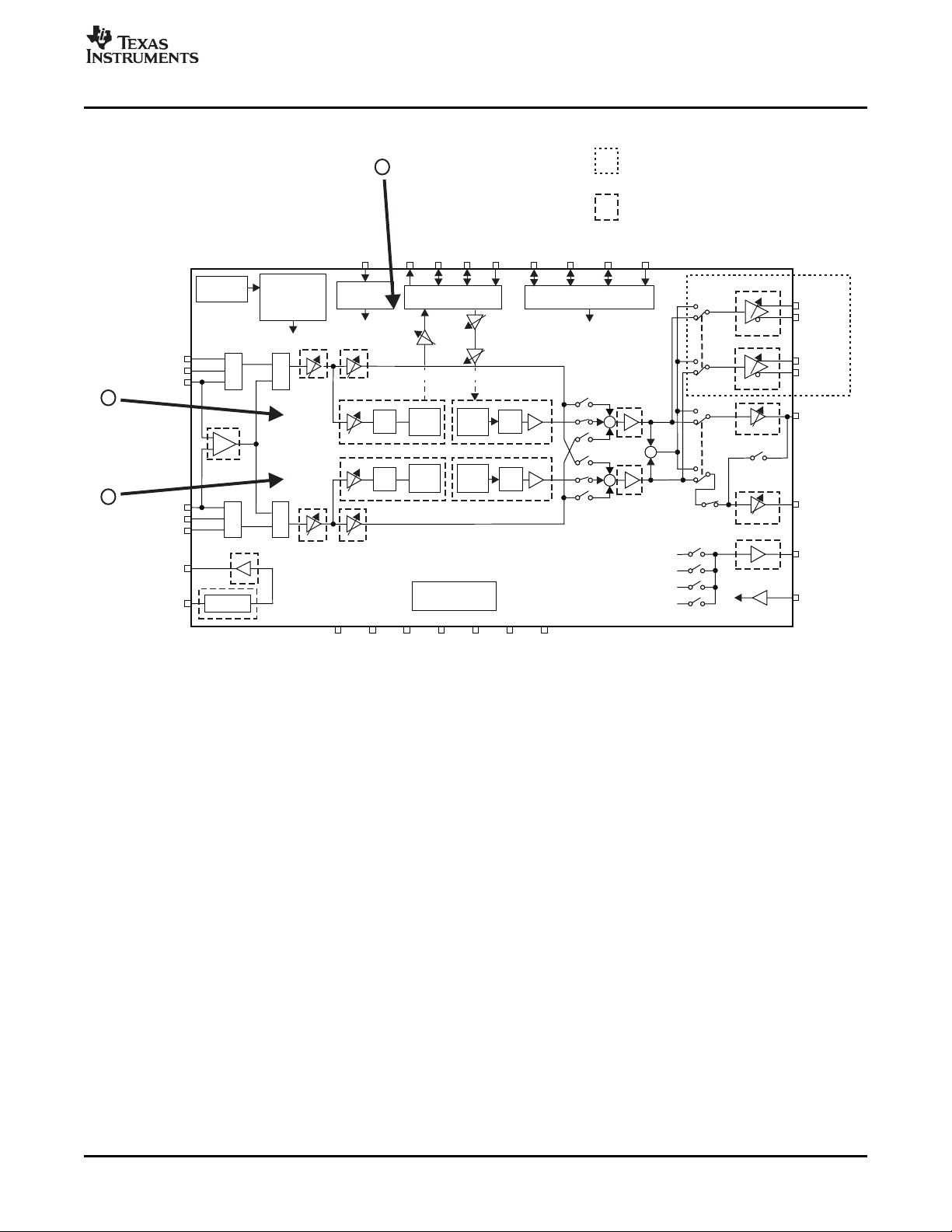
Figure 3-8 shows the EVM modules that correspond to the record function.
Gain Control for ADC Input Options
Figure 3-8. EVM Modules Corresponding to Record Function
Gain Control for ADC Input Options
Move the L-ch (PG3) and R-ch (PG4) sliders to adjust the gain of the incoming analog signal inputs to the
ADC.
• The L-ch slider manipulates the programmable gain amp (PG3) placed in front of the ADC.
• The R-ch slider controls the programmable gain amp (PG4) placed in front of the ADC.
Digital Mute (ATR) Options
Click the respective Digital mute (ATR) checkboxes if a mute function is needed for the ADC digital output.
• The mute checkbox enables a digital soft mute on the ADC for each channel.
• Mute waiting control enables a mute control.
Digital Out Mute Control Options
Select the Digital out mute control drop-down menu to enable the mute time control.
• Apply wait or no wait for the ADC mute.
SBAU127 – July 2007 Set-Up Guide 27
Submit Documentation Feedback
Page 28
www.ti.com
Digital Out Mute Control Options
3.2.3.3 Playback
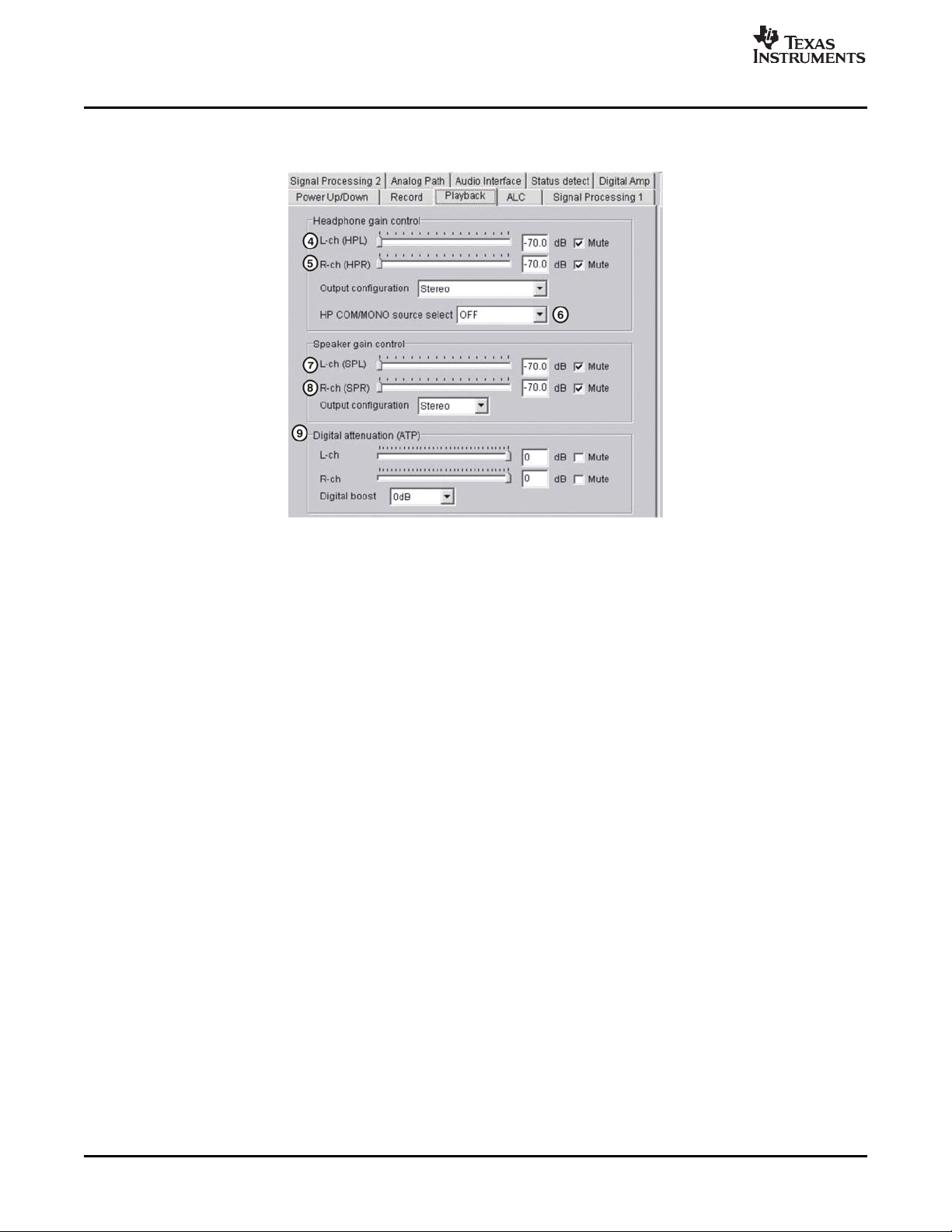
The Playback function is shown in Figure 3-9 .
Figure 3-9. Playback Function Menu Tab
28 Set-Up Guide SBAU127 – July 2007
Submit Documentation Feedback
Page 29
www.ti.com
V
COM
AIN3L
AIN2L
AIN1L
AIN2R
AIN3R
AIN1R
MICB
DS
ADC
BCK
DIN
DOUT LRCK
MS/
ADR
MC/
SCL
MD/
SDA
MODE
SerialInterface(SPI/I C)
2
SCKI
AudioInterface
V
PA
PGND VCCAGND
V
DD
DGND
HPOL/
LOL
HPOR/
LOR
SPOLP
SPOLN
SPORP
SPORN
HDTI
MUX1
DAL
ADL
DAR
HPCOM/
MONO
COM
HPR
HPL
HPC
LOUT
ROUT
+30dBto
12dB-
+30dBto
12dB-
PG5
V
IO
MONO
MCB
COM
PG1
PG3
PG4
MONO
ADR
D2S
MUX3
MUX2
MUX4
0dBto
21dB-
0dBto
21dB-
PG6
PG2
0dB/
+20dB
0dB/
+20dB
Digital
Filter
Digital
Filter
Digital
Filter
Digital
Filter
MXL
MXR
HPOR
HPOL
COM
V
COM
ATP
(0dBto 62dB,Mute)-
DGC
(0dB/+6dB/+12dB/+18dB)
SilentPopNoise
Controller
ModuleofPossiblePowerUp/Down
PCM3794AhasnoSpeakerOutput
SW1
SW2
SW3
SW6
SW5
SW4
V
COM
PowerOn
Reset
Power
Up/Down
Manager
Clock
Manager
AnalogInputR-Channel
AnalogInputL-Channel
ATR
(Mute)
DS
ADC
DS
DAC
DS
DAC
+
+
+
+6dBto
70dB-
+6dBto
70dB-
+6dBto 70dB-
+6dBto 70dB-
SPL
SPR
MicBias
4
5
6
7
8
9
Figure 3-10 shows the corresponding modules for the playback function.
Headphone Gain Control Options
Headphone Gain Control Options
Move the L-ch (HPL) and R-ch (HPR) sliders to adjust the gain of the analog output from the headphone
amplifier.
Select the Output configuration drop-down menu to select either stereo or mono output.
• The L-ch slider controls the Headphone/Line amp gain
• The R-ch slider controls the Headphone/Line amp gain
• Select the output channel to be stereo, mono (single-ended), or mono (differential)
• The HP com drop-down list determines the HPCOM/MONO pin function.
Speaker Gain Control Options
Move the L-ch (SPL) and R-ch (SPR) sliders to adjust the gain of the analog output from the speaker
amplifier.
Select the Output configuration drop-down menu to select either stereo or mono output.
• The L-ch slider controls the speaker amp gain
• The R-ch slider controls the speaker amp gain
• Select the output channel to be either stereo or mono
Figure 3-10. Modules Corresponding to Playback Function
SBAU127 – July 2007 Set-Up Guide 29
Submit Documentation Feedback
Page 30
www.ti.com
OutputAmplitude
InputAmplitude
Compression
( 2dB, 6dB, 12dB)- - -
Expansion
(0dB,+6dB,+14dB,+24dB)
0dB
0dB
Digital Attenuation (ATP) Options
Digital Attenuation (ATP) Options
Move the L-ch and R-ch sliders to adjust the gain of the incoming digital signals prior to conversion by the
DAC.
• The L-ch slider adjusts the DAC digital attenuator level
• The R-ch slider controls the DAC digital attenuator level
• Select the output channel to be either stereo or mono
• The digital boost option enables a gain control of 0dB, +6dB, +12dB, or +18dB for the DAC digital input
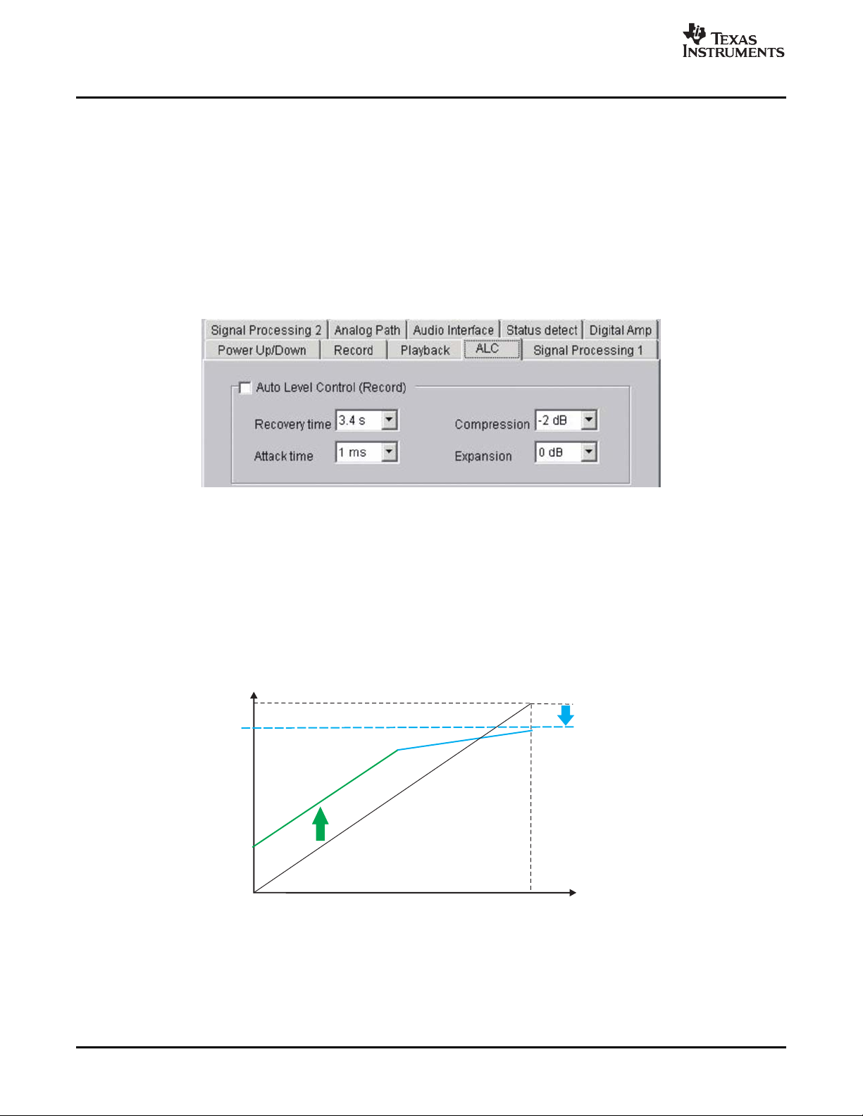
3.2.3.4 ALC (Automatic Level Control)
Figure 3-11 shows the Automatic Level Control (ALC) function menu tab.
Figure 3-11. ALC Function Menu Tab
Auto Level Control (Record) Options
Select Recovery time and Attack time using the respective drop-down menu and corresponding gain
control for each option to use the automatic level control function.
ALC compression and expansion characteristics are shown in Figure 3-12 .
Compression is defined as avoiding degradation of sound quality by saturation when there are strong
or excessively large sound data input.
Expansion means to boost weak or low input data in order to adjust the moderate amplitude level for
recording.
Figure 3-12. ALC Compression and Expansion Characteristics
Set-Up Guide30 SBAU127 – July 2007
Submit Documentation Feedback
Page 31

www.ti.com
3.2.3.5 Signal Processing I
15
10
5
0
5
10
15
-
-
-
Amplitude(dB)
10 100
1k
10k 100k
Frequency(Hz)
Figure 3-13 illustrates the Signal Processing 1 function menu tab.
Source Options
Figure 3-13. Signal Processing 1 Function Menu Tab
Source Options
Select the Source input to choose either the audio processing unit digital input (DAC) or digital output
(ADC). Internal audio processing can be applied to either the DAC or the ADC. This option also allows
users to choose an audio source.
Output Options
Select the Source drop-down menu to choose between a stereo or mono configuration.
• The output configuration can be selected by choosing stereo or mono.
Tone Control Options
Move the Bass, Mid, and Treble sliders to adjust the tone control gain. The tones are controlled by the
respective tone sliders. A three-band tone control characteristic plot is shown in Figure 3-14 .
Figure 3-14. Three-Band Tone Control (Bass, Mid, Treble)
SBAU127 – July 2007 Set-Up Guide 31
Submit Documentation Feedback
Page 32

www.ti.com
3D Effect Options
3D Effect Options
By implementing a 3D effect in this option box, the PCM3793A is enabled to provide 3D sound to the
headphone and speaker outputs with low power consumption during either ADC or DAC operation. Check
the 3D effect, then select an Effect type and an Efficiency drop-down menu to obtain the desired 3D
enhancement.
Effect type means the selection of a band-pass filter (BPF); the BPF filters the sound, and enables a high
percentage of heavy 3D enhancements to be applied to the signal.
Effect type and efficiency are controlled through the use of checkboxes.
Notch Filter 1 Coefficient, Notch Filter 2 Coefficient Options
In some applications, incoming noise such as motor control noise, CCD noise and other mechanical noise
may not be negligible. The PCM3793A provides a very useful function to reduce such interference with the
notch filter function.
When the checkbox of Notch Filter 1 Coefficient or Notch Filter 2 Coefficient is checked, coefficient a1and
a2of the notch filter can be programmed at each edit box.
Load the values of fc, fband fSinto the Filter Calculator group box.
Click Apply to Filter 1 or Apply to Filter 2. The calculated coefficient will then appear in the a1and a2edit
box.
Finally, click the Update button for each Notch filter coefficient. To complete the notch filter operation, the
Update button must be clicked.
Note that Update step is required each time new or different parameters are loaded to the dialog box.
Follow these steps to update the notch filter coefficient:
Step 1. Click the checkbox of Notch Filter 1 Coefficient or Notch Filter 2 Coefficient.
Step 2. Input the parameter values fc, fband fS.
Step 3. Click Apply to Filter 1 or Apply to Filter 2.
Step 4. Update for each notch filter coefficient.
Each coefficient is calculated using the following equations.
a1= –(1 + a2)cos( ωo)
a2= [1 – tan( ωb/2)] / [1 + tan( ωb/2)]
where:
• fS= sampling frequency
• fc= center frequency
• fb= bandwidth
• ωo= 2 π fc/fSrepresents the angular center frequency
• ωb= 2 π fb/fSis the parameter to adjust bandwidth
Here are several example coefficient calculations using Equation 3-1 and Equation 3-2 . These
measurements are also shown in Figure 3-16 .
Given: fS= 16kHz, fc= 0.5kHz, fb= 0.2kHz
a2= 0.924390492 (converted decimal to hex: 3B29h)
a1= –1.887413868 (converted decimal to hex: 8735h)
a2: F[215:208] = 3Bh, F[207:200] = 29h
a1: F[115:108] = 87h, F[107:100] = 35h
32 Set-Up Guide SBAU127 – July 2007
Submit Documentation Feedback
Page 33

www.ti.com
Amplitude(dB)
Frequency(Hz)
0dB
-3dB
f :CenterFrequency
c
f :BandwidthFrequency
b
Notch Filter 1 Coefficient, Notch Filter 2 Coefficient Options
Figure 3-15 illustrates the notch filter characteristic. All users can select any frequencies that can be used
by the application system based on the notch filter coefficient theory discussed here.
Figure 3-15. Notch Filter Characteristic Model
Figure 3-16. Example of Measured Notch Filter Characteristic
SBAU127 – July 2007 Set-Up Guide 33
Submit Documentation Feedback
Page 34

www.ti.com
DAC Oversampling Control Options
3.2.3.6 Signal Processing 2
The Signal Processing 2 Function menu tab is shown in Figure 3-17 .
DAC Oversampling Control Options
Select the DAC oversampling control menu to determine the DAC oversampling rate. The oversampling
control can be set to either 128f
The DAC oversampling rate range (for 192f
frequency of input data is lower than 24kHz. This oversampling rate moves the out-of-band noise caused
by the delta-sigma modulator to a higher frequency domain.
Figure 3-17. Signal Processing 2 Function Menu Tab
or a range of 192f
S
, 256f
S
, 256f
S
, and 384f
S
, and 384f
S
) will be selected when the sampling
S
.
S
Zero Cross Control Options
Select the Zero cross control to enable the zero crossing function. When zero crossing is enabled, digital
attenuation and the analog volume level change at the zero crossing point to avoid an audible zipper
noise.
De-Emphasis Filter Options
Select the De-emphasis filter option menu to enable the de-emphasis filter. De-emphasis can be disabled
or enabled for an appropriate sampling frequency.
High-Pass Filter Options
Choose the High Pass Filter menu to determine the center frequency (fc) of the incoming analog signal
inputs to the ADC.
The cutoff frequency of the ADC high-pass filter is provided as a sampling frequency of 48kHz in this drop
down menu, so that the cutoff will be scaled down to the corresponding value when sampling frequencies
other than 48kHz (such as 16kHz or 22.05kHz) are used.
The ADC high-pass filter cutoff frequency can be set from this option.
Set-Up Guide34 SBAU127 – July 2007
Submit Documentation Feedback
Page 35

www.ti.com
3.2.3.7 Analog Path
Figure 3-18 shows the Analog Path Function menu.
High-Pass Filter Options
Figure 3-18. Analog Path Function Menu Tab
SBAU127 – July 2007 Set-Up Guide 35
Submit Documentation Feedback
Page 36

www.ti.com
V
COM
AIN3L
AIN2L
AIN1L
AIN2R
AIN3R
AIN1R
MICB
DS
ADC
BCK
DIN
DOUT LRCK
MS/
ADR
MC/
SCL
MD/
SDA
MODE
SerialInterface(SPI/I C)
2
SCKI
AudioInterface
V
PA
PGND VCCAGND
V
DD
DGND
HPOL/
LOL
HPOR/
LOR
SPOLP
SPOLN
SPORP
SPORN
HDTI
MUX1
DAL
ADL
DAR
HPCOM/
MONO
COM
HPR
HPL
HPC
LOUT
ROUT
+30dBto
12dB-
+30dBto
12dB-
PG5
V
IO
MONO
MCB
COM
PG1
PG3
PG4
MONO
ADR
D2S
MUX3
MUX2
MUX4
0dBto
21dB-
0dBto
21dB-
PG6
PG2
0dB/
+20dB
0dB/
+20dB
Digital
Filter
Digital
Filter
Digital
Filter
Digital
Filter
MXL
MXR
HPOR
HPOL
COM
V
COM
ATP
(0dBto 62dB,Mute)-
DGC
(0dB/+6dB/+12dB/+18dB)
SilentPopNoise
Controller
ModuleofPossiblePowerUp/Down
PCM3794AhasnoSpeakerOutput
SW1
SW2
SW3
SW6
SW5
SW4
V
COM
PowerOn
Reset
Power
Up/Down
Manager
Clock
Manager
AnalogInputR-Channel
AnalogInputL-Channel
ATR
(Mute)
DS
ADC
DS
DAC
DS
DAC
+
+
+
+6dBto
70dB-
+6dBto
70dB-
+6dBto 70dB-
+6dBto 70dB-
SPL
SPR
MicBias
12
13
14
15
16
17
11
10
SwitchesSW1toSW6
Analog Input Options
Figure 3-19 illustrates the modules that correspond to the analog path function.
Figure 3-19. Modules Corresponding to Analog Path Function
Analog Input Options
This option selects the appropriate MUX for the respective left or right channel.
• MUX1 selects the L-channel source (AIN1/AIN2/AIN3).
• MUX2 selects the R-channel source (AIN1/AIN2/AIN3).
D2S Select Options
The analog input can be configured as single-end or differential. Select the D2S drop-down menu to
choose between differential or single-ended inputs. If differential is selected, AIN1L and AIN1R are used
as differential inputs.
Analog Mixer Options
Mic Boost Options
The analog input, DAC output, and other channels of the analog input can be combined as an analog
mixer source. To combine the sources, select the Analog Mixer menu to combine the DAC output and
incoming stereo or mono analog signal input through PG1/PG5 or PG2/PG6.
This checkbox sets (or resets) the +20dB microphone pre-amp PG1 (L-ch) or PG2 (R-ch).
Set-Up Guide36 SBAU127 – July 2007
Submit Documentation Feedback
Page 37

www.ti.com
PG5 Gain and PG6 Gain Options
PG5 gain (for the left channel) or PG6 (for the right channel) can be adjusted from the available
drop-down menu.
3.2.3.8 Audio Interface
Figure 3-20 shows the Audio Interface Function menu.
PG5 Gain and PG6 Gain Options
Audio Interface Setting 1 Options
Use this section of the menu to set the audio data format for the DAC input and ADC output, and set the
mode as Master or Slave. Bit length is fixed at 16 bits.
Audio Interface Setting 2 Options
Use this section of the menu when working in Master mode.
• MSR: sets system clock rate
• NPR: sets system clock divider rate
• BCK: chooses between normal and burst BCK output
Burst operation of BCK in master mode will contribute to greater overall reduction in power consumption.
See the PCM3793A data sheet for the possible combinations of these register settings.
Figure 3-20. Audio Interface Function Menu Tab
SBAU127 – July 2007 Set-Up Guide 37
Submit Documentation Feedback
Page 38

www.ti.com
HP Detection Options
3.2.3.9 Status Detect
The Status Detect function is shown in Figure 3-21 .
Figure 3-21. Status Detect Function Menu Tab
HP Detection Options
Use this section of the menu to enable or disable the HP insertion detection process. You can also the
HDTI pin logical polarity using the drop-down list box.
HP COM Short Detection Options
This section of the menu allows you to enable or disable HP COM port short detection. When short
detection recovery is set to Release, the status bit will automatically reset to '0'.
HP Short Detection, L-Ch; HP Detection, R-Ch
These sections of the menu enable or disable HP short detection for the left channel and right channel,
respectively. When short detection recovery is set to Release, the status bit will automatically reset to '0'.
Speaker Short Detection, L-Ch; Speaker Short Detection, R-Ch
These menu sections enable or disable speaker short detection for the left channel and right channel,
respectively. When short detection recovery is set to Release, the status bit will automatically reset to '0'.
Set-Up Guide38 SBAU127 – July 2007
Submit Documentation Feedback
Page 39

www.ti.com
Speaker Short Detection, L-Ch; Speaker Short Detection, R-Ch
3.2.3.10 Digital Amplifier
Figure 3-22 shows the Digital Amplifier function.
Figure 3-22. Digital Amplifier Function Menu Tab
Setting the operating speed of the Class-D speaker amplifier depends on the performance requirements;
click the checkbox to enable this function. Spectrum Spreading control (with Low, Mid, or High options)
and the Switching frequency (1.5MHz to 3MHz) can be selected here. Using this feature will help reduce
EMI noise. As the spectrum spreading control moves to high, the effect will be remarkable. Note, however,
that the signal-to-noise ratio (SNR) performance of the speaker output is affected by this function.
3.2.4 LC89052T (DIR: Digital Audio I/F Receiver) Control Window
Figure 3-23 illustrates the LC89052 Interface format choices.
Figure 3-23. LC89052 Interface Format Selection Options
3.2.4.1 Audio Clock/Data Control Options
There are several options available for the audio clock and data control features in the
DEM-DAI3793A/3794A EVM software.
For the system audio clock control, users can select any of these options:
• PLL SCK: Selects the system clock rate for the PCM3793A.
• XIN SCK or E-SCK: Selects the crystal oscillator frequency on Daughter Card #2
• CKOUT Div: Selects the dividing rate for CKOUT
The serial audio data format is controlled by the other part of the drop-down menu; see Figure 3-23 .
Select the data format for the DAC interface of the PCM3793A (it should match with the DAC setting on
the Audio Interface tab).
SBAU127 – July 2007 Set-Up Guide 39
Submit Documentation Feedback
Page 40

www.ti.com
Speaker Short Detection, L-Ch; Speaker Short Detection, R-Ch
3.2.5 Register Setting History
When any checkboxes are selected on any tab of the software GUI (including power up/down operation,
corresponding resistor address, and so forth), the register value is automatically written into the register
setting history panel. These parameters can then be saved, allowing users to identify a particular
sequence setting that was sent to the device under test.
Any operating sequence settings can be saved as a comma-separated value (*.csv) file, with an
identifiable name. This archive feature is useful when the same sequence settings are required for
continued testing. The list of available *.csv files refreshes and displays when the Clear button is clicked.
Figure 3-24 shows the Register Setting History display window.
Figure 3-24. Register Setting History Window
Set-Up Guide40 SBAU127 – July 2007
Submit Documentation Feedback
Page 41

www.ti.com
3.2.5.1 Modifying a .csv File
The .csv file stores a sequence of register settings for the PCM3793A. To load a given register setting, it
should be written in hex code, as shown in Figure 3-25 ; use the left row for resistor addresses and the
right row for resistor values.
Speaker Short Detection, L-Ch; Speaker Short Detection, R-Ch
Figure 3-25. Opening and Modifying a .csv File
A sleep line can be inserted for implementing an interval (or wait) time until executing the next line of the
file. If the cell is blank, no wait time will be executed. Files can be imported and exported using the Open
script and Save register snapshot options.
SBAU127 – July 2007 Set-Up Guide 41
Submit Documentation Feedback
Page 42

www.ti.com
Speaker Short Detection, L-Ch; Speaker Short Detection, R-Ch
3.2.6 Register Direct Access
Figure 3-26 illustrates the register direct access dialog.
Read function:
The Read function is only available in I2C mode. The register value can be read in I2C mode. To read
the value, enter the Address number (in hex code format) in the left box and click the Read button.
Data corresponding to the address appears.
Write function:
This window also enables the user to write the register value directly. Enter the Address number and
data (both in hex code format) in the respective fields and click the Write button.
Figure 3-26. Register Direct Access Dialog
42 Set-Up Guide SBAU127 – July 2007
Submit Documentation Feedback
Page 43

Switches and Connectors
This chapter reviews the DEM-DAI3793A/3794A EVM switch and jumper configuration.
Topic .................................................................................................. Page
4.1 Overview .................................................................................. 44
4.2 Motherboard ............................................................................. 44
4.3 Daughter Card #1 (PCM3793A) .................................................... 46
4.4 Daughter Card #2 (DIR: LC89052T and DIT: DIT4096) .................... 48
Chapter 4
SBAU127 – July 2007
SBAU127 – July 2007 Switches and Connectors 43
Submit Documentation Feedback
Page 44

www.ti.com
Overview
4.1 Overview
Figure 4-1 shows the location of the switches and connectors on the EVM board.
Note: Silkscreen symbol CN320 is not printed on the motherboard, but it is located in the position described.
Figure 4-1. EVM Configuration
4.2 Motherboard
Table 4-1 through Table 4-4 list the connector references for the DEM-DAI3793A/3794A EVM
motherboard.
Table 4-1. Main Power Supply and Regulator
Connectors Main Power Supply and Regulator
CN101 +6V to 10V Main Power Supply
CN102 GND
Table 4-2. Power-Supply Terminals for PCM3793A
Power-Supply Pins
Connectors PCM3793A Power-Supply Pins
CN103 V
CN104 Not used. Do not care about short or open.
CN105 V
CN106 V
CN107 V
PA
CC
DD
IO
Switches and Connectors44 SBAU127 – July 2007
Submit Documentation Feedback
Page 45

www.ti.com
Table 4-3. Audio I/O
Connectors Audio I/O Pins
CN108 Analog audio input for AIN3L
CN109 Analog audio input for AIN3R
CN110 Analog audio output for HPOL/LOL
CN111 Analog audio output for HPOR/LOR
CN112 Analog audio output for HPCOM/MONO
CN113 Not used
CN114 Analog audio input for AIN1L/AIN2L (Selected by JP12:1-2 for
AIN1L, 2-3 for AIN2L on Daughter Card #1)
CN115 Analog audio input for AIN1R/AIN2R (Selected by JP13:1-2 for
AIN1R, 2-3 for AIN2R on Daughter Card #1)
CN116 Not used
CN117 Not used
U301 TOSLINK™. S/PDIF Optical output
CN301 S/PDIF coaxial output
SW301 Toggle switch. Opt/Coax selector for S/PDIF output
U302 TOSLINK. S/PDIF Optical output
CN302 S/PDIF coaxial input
CN305 2x9 header pins to connect digital audio I/F for ADC/DAC. If using
external signal source, all shorting plugs should be removed.
CN306 BNC connector to provide external clock for LC89052T (DIR: S/PDIF
receiver) on Daughter Card or PCM3793 directly as E-SCK.
CN307 2x5 header pins. System clock and bit clock selection to provide
DIT4096 (DIT: S/PDIF transmitter). SCK and BCK should be provided
from LC89052T as initial setting.
CN308, CN309–CN316 2x9 header pins and SMA connecters (x8) for connecting digital
audio I/F with external devices or equipment. If using this feature, all
shorting plugs on CN305 should be removed.
CN317 3x10 header pins. Path of I2C/SPI-interface selection (via USB or
parallel port). Selected USB port for initial configuration. (Parallel
port is not available.)
CN320 2x3 header pins. Word (L/R) clock selection (Master or Slave mode).
Selected Slave mode as initial.
Motherboard
Table 4-4. I/F Controller (MSP430 , TUSB3410 )
Connectors I/F Controller(MSP430, TUSB3410)
CN201 USB connector type-B
CN202 JTAG port
SW201 Push switch. RESET for MSP430/TUSB3410
SBAU127 – July 2007 Switches and Connectors 45
Submit Documentation Feedback
Page 46

www.ti.com
AINL
Connectedto
CN114ofmotherboard
Connectedto
CN115ofmotherboard
Connectedto
CN108ofmotherboard
Connectedto
CN109ofmotherboard
AINL
AINR
R-Ch
JP10
JP11
JP8
JP9
JP12
JP13
J2
(Monomic)
PCM3793A
AIN1L
AIN2L
AIN1R
AIN2R
AIN3L
AIN3R
1
2
3
1
2
3
1
2
3
1
2
3
1
2
3
1
2
3
AINR
J1
(Stereomic)
R-Ch
L-Ch
L-Ch
Daughter Card #1 (PCM3793A)
4.3 Daughter Card #1 (PCM3793A)
Table 4-5 lists the connector references for the first DEM-DAI3793A/3794A EVM daughter card.
Simplified descriptions of the analog input and output configuration for Daughter Card #1 are shown in
Figure 4-2 and Figure 4-3 .
Table 4-5. Analog Input and Output—Daughter Card #1
Connectors Analog Input and Output of Daughter Card #1
J1 Stereo microphone input
J2 Monaural microphone input
J3 Speaker output terminal for L-ch
J4 Speaker output terminal for R-ch
J5 Headphone output (Cap-less)
J6 Headphone output
JP5 System clock select. 1-2: External clock; 3-4: SPDIF
JP8 1-2: AIN1L / 2-3: JP10
JP9 1-2: AIN1R / 2-3: JP11
JP10 1-2: JP8 / 2-3: J2
JP11 1-2: J1 / 2-3: J2
JP12 Analog input select L-channel 1-2: AIN1L / 2-3: AIN2L
JP13 Analog input select R-channel 1-2: AIN1R / 2-3: AIN2R
JP18 Headphone detection select. 1-2: J5 or J6 / 2-3: Motherboard
46 Switches and Connectors SBAU127 – July 2007
Figure 4-2. Analog Input Configuration (Daughter Card #1)
Submit Documentation Feedback
Page 47

www.ti.com
Connectedto
CN112ofmotherboard
Connectedto
CN110ofmotherboard
Connectedto
CN111ofmotherboard
J5
HPOUT(Cap-less)
MONO
LINEOUT
(L-Ch)
LINEOUT
(R-Ch)
SPOLN
SPOLP
SPORN
SPORP
HPCOM/MONO
HPOR/LOR
HPOL/LOL
J6
HPOUT
J4
SPOUT(R-Ch)
J3
SPOUT(L-Ch)
PCM3793A
Figure 4-3. Analog Output Configuration (Daughter Card #1)
CAUTION
Do not insert a headphone to J5 and J6 at the same time. Doing so connects
resistors in parallel.
Daughter Card #1 (PCM3793A)
SBAU127 – July 2007 Switches and Connectors 47
Submit Documentation Feedback
Page 48

www.ti.com
Daughter Card #2 (DIR: LC89052T and DIT: DIT4096)
4.4 Daughter Card #2 (DIR: LC89052T and DIT: DIT4096)
Table 4-6 lists the connector references for the second DEM-DAI3793A/3794A EVM daughter card.
Table 4-6. Analog Input and Output—Daughter Card #2
Connectors Analog Input and Output of Daughter Card #2
SW001 Toggle switch. Opt/Coax selector for S/PDIF input
SW002 Toggle switch. Reset/Power-down LC89052T and DIT4096
SW003 Clock source selection for LC89052T (Onboard crystal oscillator or
SW004 DIP switch. Sets channel-status data of the DIT4096
SW005 DIP switch. Sets the DIT4096 system clock and data format. Note
(1)
See the DIT4096 product data sheet (TI literature number SBOS225 , available for download from
the TI web site ) for further information.
Table 4-7 describes the audio clock and data control format options for Daughter Card #2.
Table 4-7. Audio Clock and Input Data Control
CLK0 CLK1 System Clock
L L Not used
L H 256f
H L 384f
H H 512f
FMT0 FMT1 Input Data Format
L L 24-bit, left-justified, MSB-first
L H 24-bit, I2S (initial setting)
H L 24-bit, right-justified, MSB-first
H H 16-bit, right-justified, MSB-first
external source from CN306 of motherboard)
OFF state of this switch sets a HIGH level. Channel-status data can
be set up if needed. It is also possible to connect a microcontroller.
that the OFF state of this switch sets a HIGH level.
Format—Daughter Card #2
(1)
. Note that the
(initial setting)
S
S
S
Switches and Connectors48 SBAU127 – July 2007
Submit Documentation Feedback
Page 49

Chapter 5
SBAU127 – July 2007
Evaluation and Measurements
This chapter discusses how to set up jumpers on the DEM-DAI3793A/3794A EVM motherboard for
performance evaluation using the Audio Precision SYS-2722
process of measuring dynamic characteristics is then presented, along with example characteristic data.
Topic .................................................................................................. Page
5.1 Slave Mode With Audio Precision SYS-2722 (Default Setting) ......... 50
5.2 Master Mode with Audio Precision SYS-2722 ............................... 52
5.3 Combined Master and Slave Modes With PSIA-2722 ...................... 54
5.4 Measurements for Dynamic Characteristics ................................. 55
5.5 Connection Diagram for Practical Applications ............................ 61
®
or PSIA-2722
®
audio analyzers. The
SBAU127 – July 2007 Evaluation and Measurements 49
Submit Documentation Feedback
Page 50

www.ti.com
SCKI
BCK
LRCK
DOUT
DIN
DAC
DIR:LC89052T
ADC
PCM3793A
Daughtercard#2 Daughtercard#1
DIT:DIT4096
U302
CN302
U301
CN301
SW301
SW001
Clock
Manager
AudioInterface
Slave Mode With Audio Precision SYS-2722 (Default Setting)
5.1 Slave Mode With Audio Precision SYS-2722 (Default Setting)
These jumper configurations for the DEM-DAI3793A/3794A EVM motherboard are the default device
settings. Simple evaluation using the Audio Precision SYS-2722 (as shown in Figure 5-1 ) is easily
managed.
Figure 5-1. Slave Mode Configuration With SYS-2722
To put the DEM-DAI3793A/3794A EVM motherboard into the default slave mode configuration, connect
the S/PDIF input and output to optical jumper U302 (or coaxial jumper CN302) and jumper U301 (or
jumper CN301). Then select SW301 and SW001, respectively. Refer to the jumper combination shown in
Figure 5-2 .
50 Evaluation and Measurements SBAU127 – July 2007
Submit Documentation Feedback
Page 51

www.ti.com
Shortplug
Shortplug
Allopen
Allshort
Shortplug
Shortplug
CN305
CN307
T-SCLK
GND
T-BCK
T-SCK
T-LRCK
T-BCK
TX-DATA
T-LRCK
E-SCLK
TX-DATA
R-SCLK
R-SCLK
R-BCK
R-BCK
R-LRCK
R-LRCK
RX-DATA
RX-DATA
E-SCK
SCK
T-SCLK
BCK
T-BCK
fromU003(DIR:LC89052T)onDaughterCard#2
fromU003(DIR:LC89052T)onDaughterCard#2
CN308
CN320
Slave Mode With Audio Precision SYS-2722 (Default Setting)
Figure 5-2. Jumper Configuration for Slave Mode (Default)
SBAU127 – July 2007 Evaluation and Measurements 51
Submit Documentation Feedback
Page 52

www.ti.com
SCKI
BCK
LRCK
DOUT
DIN
DAC
DIR:LC89052T
ADC
PCM3793A
Daughtercard#2 Daughtercard#1
DIT:DIT4096
U302
CN302
U301
CN301
SW301
SW001
Clock
Manager
AudioInterface
Isolatedby
CN305
Master Mode with Audio Precision SYS-2722
5.2 Master Mode with Audio Precision SYS-2722
To enable the DEM-DAI3793A/3794A EVM motherboard for use in Master mode, the path of the S/PDIF
input to the PCM3793A through DIR is not available for use. LRCK and BCK change the respective output
states at the PCM3793A side in master mode; the respective jumpers of R-BCK, R-LRCK, and RX-DATA
should be removed from CN305 to avoid conflict between the input and output of these clocks.
Furthermore, in this situation, DIN to the PCM3793A is also invalid because DIR LC89052T does not
receive clocks (LC89052T cannot work in slave mode). Therefore, any analog output from the DAC is
invalid because there is no data input.
However, in this configuration, users can confirm master mode operation of both LRCK and BCK from
PCM3793A with a digital oscilloscope. Users can easily identify master mode without the use of other
external equipment such as the PSIA-2722 analyzer.
The PCM3793A has no integrated internal PLL. However, the clock manager function can provide LRCK
(fS) and BCK in master mode, as described in Figure 5-3 .
Figure 5-3. Master Mode Configuration With SYS-2722
Refer to the jumper combination shown in Figure 5-4 to put the DEM-DAI3793A/3794A EVM motherboard
into master mode configuration.
52 Evaluation and Measurements SBAU127 – July 2007
Submit Documentation Feedback
Page 53

www.ti.com
Shortplug
Shortplug
Shortplug
Allopen
Shortplug
CN305
CN307
T-SCLK
GND
T-BCK
T-SCK
T-LRCK
T-BCK
TX-DATA
T-LRCK
E-SCLK
TX-DATA
R-SCLK
R-SCLK
R-BCK
R-BCK
R-LRCK
R-LRCK
RX-DATA
RX-DATA
E-SCK
SCK
T-SCLK
BCK
T-BCK
fromU003(DIR:LC89052T)onDaughterCard#2
fromU003(DIR:LC89052T)onDaughterCard#2
CN308
CN320
Master Mode with Audio Precision SYS-2722
Figure 5-4. Jumper Configuration for Master Mode
SBAU127 – July 2007 Evaluation and Measurements 53
Submit Documentation Feedback
Page 54

www.ti.com
SCKI
BCK
LRCK
DOUT
DIN
DAC
ADC
PCM3793A
Daughtercard#1
Clock
Manager
AudioInterface
PSIA-2722
Slave
Master
Master
Slave
Combined Master and Slave Modes With PSIA-2722
5.3 Combined Master and Slave Modes With PSIA-2722
As shown in Figure 5-5 , the DEM-DAI3793A/3794A EVM can provide evaluation for both slave and master
modes of the PCM3793A at the same time without setup jumpers on the motherboard if the user has
access to the PSIA-2722 analyzer.
Figure 5-5. Combined Master and Slave Mode Configuration with SYS-2722
Refer to the jumper combination shown in Figure 5-6 to set up the combined master and slave modes
configuration.
54 Evaluation and Measurements SBAU127 – July 2007
Submit Documentation Feedback
Page 55

www.ti.com
Shortplug
Shortplug
Shortplug
Shortplug
Allopen
CN305
CN307
T-SCLK
GND
T-BCK
T-SCK
T-LRCK
T-BCK
TX-DATA
T-LRCK
E-SCLK
TX-DATA
R-SCLK
R-SCLK
R-BCK
R-BCK
R-LRCK
R-LRCK
RX-DATA
RX-DATA
E-SCK
SCK
T-SCLK
BCK
T-BCK
fromU003(DIR:LC89052T)onDaughterCard#2
fromU003(DIR:LC89052T)onDaughterCard#2
CN308
CN320
PSIA-2722
Measurements for Dynamic Characteristics
Figure 5-6. Jumper Configuration for Combined Master and Slave Modes
5.4 Measurements for Dynamic Characteristics
Typical dynamic performance graphs for digital-to-analog converters (DACs) generally represent four
performance characteristics (in addition to other specifications): total harmonic distortion and noise
(THD+N); signal-to-noise ratio (SNR); dynamic range (DR); and channel separation. These graphs also
specify the test environment and measurement conditions required in order to meet typical performance
values defined in the product data sheet.
For the DEM-DAI3793A/3794A EVM, the evaluation environment specifications are:
• Equipment used: Audio Precision, System Two Cascade Plus
• Audio Data format: 16-bit Left-Justified
• SCKI / BCK / LRCK (fS): 256f
• Power supply: V
• Temperature: Room/ambient
Once the lab or test environment is configured according to these parameters, start the EVM software (as
discussed in Section 3.2 ). Click All Power On in the startup window or execute power_on.csv, and then
execute the .csv file that corresponds to the appropriate measurement path discussed in the subsequent
sections of this chapter.
DD
/ 64f
S
= V
= V
IO
CC
/ 48 kHz
S
= V
= 3.3V (Regulated down from 10V applied to the motherboard)
PA
SBAU127 – July 2007 Evaluation and Measurements 55
Submit Documentation Feedback
Page 56

www.ti.com
Measurements for Dynamic Characteristics
5.4.1 Digital-to-Analog (D/A) Performance
Measurement path: 01.Line Output and Headphone Output
csv file: 01_DAC_Line_Output_and_Headphone_Output.csv
Power Supply Parameter Filter Setting RL(k Ω ) LOL LOR
3.3V THD+N (0dBFS at 1kHz) 400Hz—20kHz AES-17 10 0.007% 0.008%
Power Supply Parameter Filter Setting RL( Ω ) HPOL HPOR
3.3V THD+N (40mW, HP 400Hz—20kHz AES-17 16 0.028% 0.027%
Table 5-1. D/A Line Output Parameters
SNR (BPZ input) 22Hz—20kHz SPCL + 10 93.1dB 93.0dB
A-weighting
DR (–60dBFS input) 22Hz—20kHz SPCL + 10 93.1dB 92.9dB
A-weighting
Channel Separation 22Hz—20kHz AES-17 10 90.5dB 90.4dB
(BPZ input for target
channel)
Table 5-2. 16 Ω Headphone Output Inserted in Headphone Jack J6
volume = –1dB)
SNR (BPZ input) 22Hz—20kHz SPCL + 16 93.1dB 93.0dB
A-weighting
DR (–60dBFS input) 22Hz—20kHz SPCL + 16 93.4dB 93.1dB
A-weighting
To obtain the performance results shown in Table 5-1 and Table 5-2 , the speaker module should be
powered down, and other functions should be set with these parameters:
• Speaker Amp: Disabled
• ADC L-channel and ADC R-channel: Disabled
• ALC: Off
• Volume: 0dB
• Analog mixing: Disabled
• R
= 10k Ω for the line output
L
• R
= 16 Ω inserted in the J6 headphone jack for the headphone output
L
The bundled .csv file automatically sets the device to these conditions.
Note: The headphone volume should be changed from 0dB to –1dB and the signal input level of
the Audio Precision analyzer should be changed to 40mW output power when THD+N is
measured at 16 Ω .
See Appendix A : Line Output and Headphone Output for a signal flow block diagram.
Evaluation and Measurements56 SBAU127 – July 2007
Submit Documentation Feedback
Page 57

www.ti.com
5.4.2 Analog-to-Digital (A/D) Performance
Measurement path: 17.Line Input (AIN3L/AIN3R)
csv file: 17_ADC_Line_Input.csv
Power Supply Parameter Filter Setting Left Channel Right Channel
3.3V THD+N ( –1dB at 1kHz) 400Hz—20kHz AES-17 0.009% 0.009%
To obtain the performance results shown in Table 5-3 , the speaker/headphone module should be powered
down, and other functions should be set with these parameters:
• Headphone and Speaker Amp: Disabled
• DAC L-channel and DAC R-channel: Disabled
• ALC: Off
• Mic boost: 0dB
• Analog mixing: Disabled
• All PGA: 0dB
The bundled .csv file automatically sets the device to these conditions.
See Appendix A : Line Input (AIN3L/AIN3R) for a signal flow block diagram.
Measurements for Dynamic Characteristics
Table 5-3. A/D Line Input Parameters
SNR (BPZ input) 22Hz—20kHz SPCL + 90.4dB 90.5dB
A-weighting
DR (–60dBFS input) 22Hz—20kHz AES-17 + 90.6dB 90.3dB
A-weighting
Channel Separation 22Hz—20kHz AES-17 87.8dB 87.8dB
(BPZ input for target channel)
5.4.3 Speaker Output Power Performance
Measurement path: 07.Stereo Speaker Output
csv file: 07_DAC_Stereo_Speaker_Output_8ohms.csv
Power Supply Parameter Speaker Volume RL( Ω ) SPOL SPOR
3.3V Output Power +6dB 8 594.2mW 594.1mW
To obtain the performance results shown in Table 5-4 , the headphone module should be powered down,
and other functions should be set with these parameters:
• Headphone Amp: Disabled
• ADC L-channel and ADC R-channel: Disabled
• Speaker volume: +6dB
• ALC: Off
• RL: 8 Ω
The bundled .csv file automatically sets the device to these conditions, except for the speaker volume;
adjust the speaker volume to +6dB manually after the .csv file is loaded.
Note: Adjust the input signal level of the Audio Precision analyzer to meet the target THD+N =
Table 5-4. Stereo Speaker Output Parameters
(THD+N = 10%)
10%.
See Appendix A : Stereo Speaker Output for a signal flow block diagram.
SBAU127 – July 2007 Evaluation and Measurements 57
Submit Documentation Feedback
Page 58

www.ti.com
Note(1):SameconfigurationatSPORN/SPORP
SPOL
SPOR
J3
J4
SnubberCircuit LCLPF
SPOLN
SPOLP
L122 Hm
L222 Hm
C11
2.2 Fm
C12
2.2 Fm
C9
0.82 Fm
C8
0.82 Fm
R6
330W
R5
330W
R
8
L
W
Audio
Analyzer
Differential
Input
J3
TP2
TP1
+
-
f =
C
» 37.5[kHz]
2 p´ ´
LC
1
(1)
Measurements for Dynamic Characteristics
5.4.3.1 LC Low-Pass Filter
Daughter Card #2 provides an LC low-pass filter (LPF) to obtain a clean analog signal from the
pulse-width modulated (PWM) output of the speaker output. This configuration is shown in Figure 5-7 .
Additionally, a snubber circuit is inserted into the signal line to achieve the best output power performance
by suppressing ringing in the PWM pulse; however, a snubber circuit will have negligible effects in the end
system.
Figure 5-7. Speaker Output Filter Configuration
Evaluation and Measurements58 SBAU127 – July 2007
Submit Documentation Feedback
Page 59

www.ti.com
5.4.4 Amplitude Versus Frequency Performance
0
20
40
60
80
100
120
140
-
-
-
-
-
-
-
Amplitude(dB)
AMPLITUDEvsFREQUENCY
0
5
10 15 20
Frequency(kHz)
BPZ(ZeroData)Input
0
20
40
60
80
100
120
140
-
-
-
-
-
-
-
Amplitude(dB)
AMPLITUDEvsFREQUENCY
0
5
10 15 20
Frequency(kHz)
-60dBInput
0
20
40
60
80
100
120
140
-
-
-
-
-
-
-
Amplitude(dB)
AMPLITUDEvsFREQUENCY
0
5
10 15 20
Frequency(kHz)
-1dBInput
5.4.4.1 A/D Spectrum
Measurement path: 17.Line Input (AIN3L/AIN3R)
csv file: 17_ADC_Line_Input.csv
Note that an unweighted filter and an AES17 bandwidth of 22Hz to 20kHz should be set to obtain precise
spectrum results.
Measurements for Dynamic Characteristics
Figure 5-8. A/D Amplitude vs Frequency Figure 5-9. A/D Amplitude vs Frequency
Result: BPZ (Zero Data) Input Result: –60dB Input
Figure 5-10. A/D Amplitude vs Frequency
Result: –1dB Input
See Appendix A : Line Input (AIN3L/AIN3R) for a signal flow block diagram.
SBAU127 – July 2007 Evaluation and Measurements 59
Submit Documentation Feedback
Page 60

www.ti.com
0
20
40
60
80
100
120
140
-
-
-
-
-
-
-
Amplitude(dB)
AMPLITUDEvsFREQUENCY
0
5
10 15 20
Frequency(kHz)
BPZ(ZeroData)Input
0
20
40
60
80
100
120
140
-
-
-
-
-
-
-
Amplitude(dB)
AMPLITUDEvsFREQUENCY
0
5
10 15 20
Frequency(kHz)
-60dBInput
0
20
40
60
80
100
120
140
-
-
-
-
-
-
-
Amplitude(dB)
AMPLITUDEvsFREQUENCY
0
5
10 15 20
Frequency(kHz)
0dBInput
0
20
40
60
80
100
120
140
-
-
-
-
-
-
-
Amplitude(dB)
AMPLITUDEvsFREQUENCY
WideRangeto130kHz
0 20 40 60 80 100 120
Frequency(kHz)
BPZ(ZeroData)Input
Measurements for Dynamic Characteristics
5.4.4.2 D/A Spectrum
Measurement path: 01.Line Output and Headphone Output
csv file: 01_DAC_Line_Output_and_Headphone_Output.csv
Note that an unweighted filter and an AES17 bandwidth of 22Hz to 20kHz should be set to obtain precise
spectrum results.
Figure 5-11. D/A Amplitude vs Frequency Figure 5-12. D/A Amplitude vs Frequency
Result: BPZ (Zero Data) Input Result: –60dB Input
Figure 5-13. D/A Amplitude vs Frequency Figure 5-14. D/A Amplitude vs Frequency
See Appendix A : Line Output and Headphone Output for a signal flow block diagram.
Evaluation and Measurements60 SBAU127 – July 2007
Result: 0dB Input
Result: Wide Range to 130kHz, BPZ (Zero
Data) Input
Submit Documentation Feedback
Page 61

www.ti.com
5.5 Connection Diagram for Practical Applications
C
7
Stereo
Headphone
R
2
C
1
C
2
C
3
C
4
C
5
C
6
Low or H igh
R
1
R
4
SCKI (7)
BCK(1)
LRCK (32)
DIN(2)
DOUT (3)
MO
DE (28)
MS/ADR (29)
MD/SDA (30)
MC/SCL (31)
V
COM
(18)
(11) SPORP
(10) SPORN
(8)HDTI
(16) HPOR/LOR
AIN1L (27)
AIN1R (26)
AIN2L (25)
AIN2R (24)
AIN3L (23)
AIN3R (22)
MICB (21)
(15) SPOLP
(14) SPOLN
(17) HPOL/LOL
(9) HPCOM/MONO
C
10
(20)V
CC
(19) AGND
(12)V
PA
C
11
(13)PGND
(4)V
IO
(5)V
DD
(6) DGND
C
8
C
9
C
13
C
14
C
12
R
3
Monaural
LineOutput
PCM3793A/94A
ToRegulator
The PCM3793A/94A Daughter Card has been configured to measure dynamic audio performance by
common audio analyzer equipment.
In a practical application (such as portable audio player or cellular phone), simple components set up as
shown in Figure 5-15 will be reasonable to save assembly and test spaces. Specific component values
are listed in Table 5-5 .
Connection Diagram for Practical Applications
C1—C6 1 μ F C12, C13 10 μ F–220 μ F
C7 1 μ F–10 μ F C14 1 μ F–10 μ F
C8 0.1 μ F R1, R2 2.2k Ω
C9, C10 1 μ F–4.7 μ F R3 33k Ω
C11 4.7 μ F–10 μ F R4 10k Ω
Table 5-5. Recommended External Parts for Basic Connection Diagram
Component Recommended Value Component Recommended Value
Figure 5-15. Basic Connection Diagram
SBAU127 – July 2007 Evaluation and Measurements 61
Submit Documentation Feedback
Page 62

www.ti.com
SPOLP/
SPORP
SPOLN/
SPORN
B
1
B
2
C
15
C
16
HDTI
V
CC
+
+
HPOL
HPOR
PGND
HPCOM
HP Jack
HDTI
HPOL
HPOR
PGND
HPCOM
HP Jack
ConventionalMode CaplessMode
V
CC
Connection Diagram for Practical Applications
5.5.1 Filter Consideration for Speaker Output
For a practical application such as a portable audio player or cellular phone, a ferrite chip bead will be a
suitable low-pass filter to the speaker output; see Figure 5-16 . Figure 5-17 describes recommended
connections for headphone output and insertion detection.
Refer to the product data sheet for further information on this application circuit. C15and C
Chip Bead : NEC/Tokin: N2012ZPS121.
Figure 5-16. Recommended Ferrite Bead Filter for Speaker Output
Figure 5-17. Connection for Headphone Output and Insertion Detection
= 1nF, B1and B2Ferrite
16
62 Evaluation and Measurements SBAU127 – July 2007
Submit Documentation Feedback
Page 63

Chapter 6
SBAU127 – July 2007
Schematic, PCB Layout, and Bill of Materials
This chapter provides the electrical and physical layout information for the DEM-DAI3793A/3794A EVM.
The bill of materials is included for component and manufacturer reference.
Topic .................................................................................................. Page
6.1 Schematics .............................................................................. 64
6.2 Printed Circuit Board Layout ...................................................... 66
6.3 Component List ........................................................................ 71
SBAU127 – July 2007 Schematic, PCB Layout, and Bill of Materials 63
Submit Documentation Feedback
Page 64

www.ti.com
Schematics
6.1 Schematics
Figure 6-1 and Figure 6-2 illustrate the schematics for the DEM-DAI3793A/3794A EVM.
Figure 6-1. PCM3793A DEM-PCM3793RHB-A Connector (Daughter Card #1)
64 Schematic, PCB Layout, and Bill of Materials SBAU127 – July 2007
Submit Documentation Feedback
Page 65

www.ti.com
Schematics
Figure 6-2. PCM3793A DEM-PCM3793RHB-A (Daughter Card #1)
SBAU127 – July 2007 Schematic, PCB Layout, and Bill of Materials 65
Submit Documentation Feedback
Page 66

www.ti.com
Printed Circuit Board Layout
6.2 Printed Circuit Board Layout
Figure 6-3 through Figure 6-7 illustrate the printed circuit board (PCB) layout for the
DEM-DAI3793A/3794A EVM.
Note: Board layouts are not to scale. These figures are intended to show how the board is laid
out; they are not intended to be used for manufacturing DEM-DAI3793A/3794A EVM
PCBs.
Figure 6-3. PCM3793A DEM-PCM3793RHB-A Board Layout—Silkscreen Side
66 Schematic, PCB Layout, and Bill of Materials SBAU127 – July 2007
Submit Documentation Feedback
Page 67

www.ti.com
Printed Circuit Board Layout
Figure 6-4. PCM3793A DEM-PCM3793RHB-A Board Layout—Component Side
SBAU127 – July 2007 Schematic, PCB Layout, and Bill of Materials 67
Submit Documentation Feedback
Page 68

www.ti.com
Printed Circuit Board Layout
Figure 6-5. PCM3793A DEM-PCM3793RHB-A Board Layout—Inner Layer 2
68 Schematic, PCB Layout, and Bill of Materials SBAU127 – July 2007
Submit Documentation Feedback
Page 69

www.ti.com
Printed Circuit Board Layout
Figure 6-6. PCM3793A DEM-PCM3793RHB-A Board Layout—Inner Layer 3
SBAU127 – July 2007 Schematic, PCB Layout, and Bill of Materials 69
Submit Documentation Feedback
Page 70

www.ti.com
Printed Circuit Board Layout
Figure 6-7. PCM3793A DEM-PCM3793RHB-A Board Layout—Solder Side
Schematic, PCB Layout, and Bill of Materials70 SBAU127 – July 2007
Submit Documentation Feedback
Page 71

www.ti.com
6.3 Component List
Table 6-1 lists the Bill of Materials for the DEM-DAI3793A/3794A EVM.
RefDes Count Description Part Number MFR
R3, R5, R6, R7, 5 330 Ω CF1/4C-33 Ω J KOA
R8
CP1—CP4 4 0.1 μ F GRM188F5E104ZA01D Murata
C8, C9, C13, C14 4 0.82 μ F ECQV1H824J Nissei
R4 1 100k Ω , CF1/4C-100k Ω J KOA
R9, R10 2 10k Ω CF1/4C-10k Ω J KOA
C3, C4, C6, C10 4 10 μ F/16V R3A-16V100M Elna
C1, C2 2 1 μ F ECEV1HA010NR Panasonic
C5 1 1 μ F/50V R3A-50V10M Elna
R1, R2 2 2.2k Ω CF1/4C-2.2k Ω J KOA
C11, C12, C15, 4 2.2 μ F/50V R3A-50V22M Elna
C16
C17, C18 2 220 μ F R3A-4V2200M Elna
L1—L4 4 22 μ H 22R223 Newport
JP5 1 2x2 Pin A1-4PA-2.54DSA Hirose
JP8—JP13, JP18 7 3-Pin A2-3PA-2.54DSA Hirose
C7 1 4.7 μ F/25V R3A-25V47M Elna
TP1—TP4 4 Test Pin LC-2-G MAC8
J1, J2 2 HSJ1493-01-040 Hosiden
J3, J4 2 MKDSN1.5/2-5.08 Phoenix Contact
J5, J6 2 HSJ1493-01-040 Hosiden
U1 1 16-bit Stereo Audio Codec, 5mm x 5mm QFN, 32-pin PCM3793A/94A Texas Instruments
Component List
Table 6-1. Bill of Materials
1
Components
SBAU127 – July 2007 Schematic, PCB Layout, and Bill of Materials 71
Submit Documentation Feedback
Page 72

Schematic, PCB Layout, and Bill of Materials72 SBAU127 – July 2007
Submit Documentation Feedback
Page 73

Reference .csv Files, Interfacing to DSPs, and Package
Topic .................................................................................................. Page
A.1 Reference .csv Files .................................................................. 74
A.2 Interfacing to DSPs ................................................................... 98
A.3 Package Information.................................................................. 99
Appendix A
SBAU127 – July 2007
Information
SBAU127 – July 2007 Reference .csv Files, Interfacing to DSPs, and Package Information 73
Submit Documentation Feedback
Page 74

www.ti.com
Reference .csv Files
A.1 Reference .csv Files
The .csv files are bundled with the DEM-DAI3793A/3794A EVM Controller. These files enable users to
execute register settings corresponding to the specific operating modes discussed in the product data
sheet by importing them into the software.
Note that each .csv file (listed in Table A-1 ) must be implemented after an All Active operation is
performed with the power_on.csv command; otherwise, these files will not work properly.
An All Active operation is recommended to start up the device, and can be executed by just clicking the All
Power On button, as discussed in Section 3.2 .
All Power Down power_off.csv
All Active power_on.csv
Playback with Digital Input
01 Line Output and Headphone Output 01_DAC_Line_Output_and_Headphone_Output.csv
02 Headphone Output with Sound Effect 02_DAC_Headphone_Output_with_Sound_Effect.csv
03 Cap Less Headphone Output 03_DAC_Cap_Less_Headphone_Output.csv
04 Headphone Output with Line Input (AIN2L/AIN2R) 04_DAC_Headphone_Output_with_Line_Input.csv
05 Headphone Output with Mono Mic Input (AIN1L, +20dB) 05_DAC_Headphone_Output_with_Mono_Mic_Input.csv
06 Headphone Output with Mono Diff Mic Input 06_DAC_Headphone_Output_with_Mono_Diff_Mic_Input.
07 Stereo Speaker Output 07_DAC_Stereo_Speaker_Output.csv
08 Mono Speaker Output 08_DAC_Mono_Speaker_Output.csv
09 Speaker Output with Line Input (AIN2L/AIN2R) 09_DAC_Speaker_Output_with_Line_Input.csv
10 Speaker Output with Mono Mic Input (AIN1L, +20dB) 10_DAC_Speaker_Output_with_Mono_Mic_Input.csv
11 Speaker Output with Mono Diff Mic Input (AIN1L/AIN1R, 11_DAC_Speaker_Output_with_Mono_Diff_Mic_Input.csv
Playback without Digital Input
12 Line Input (AIN2L/AIN2R) to Headphone Output 12_Line_Input_to_Headphone_Output.csv
13 Mono Line Input (AIN2L) to Headphone Output 13_Mono_Line_Input_to_Headphone_Output.csv
14 Mono Mic Input (AIN1L, +20dB) to Headphone Output 14_Mono_Mic_Input_to_Headphone_Output.csv
15 Mono Diff Mic Input (AIN1L/AIN1R, +20dB) to 15_Mono_Diff_Mic_Input_to_Headphone_Output.csv
16 Mono Mic Input (AIN1L, +20dB) to Speaker Output 16_Mono_Mic_Input_to_Speaker_Output.csv
Recording
17 Line Input (AIN3L/AIN3R) 17_ADC_Line_Input.csv
18 Mic Input (AIN1L/AIN1R, +20dB) 18_ADC_Mic_Input.csv
19 Mic Input (AIN1L/AIN1R, +20dB) with ALC 19_ADC_Mic_Input_with_ALC.csv
20 Mono Mic Input (AIN1L, +20dB) 20_ADC_Mono_Mic_Input.csv
21 Mono Mic Input (AIN1L, +20dB) with ALC 21_ADC_Mono_Mic_Input_with_ALC.csv
22 Mono Diff Mic Input (AIN1L/AIN1R, +20dB) 22_ADC_Mono_Diff_Mic_Input.csv
23 Mono Diff Mic Input (AIN1L/AIN1R, +20dB) with ALC 23_ADC_Mono_Diff_Mic_Input_with_ALC.csv
Table A-1. .csv Files
Operating Mode .csv File Name
(AIN1L/AIN1R, +20dB) csv
+20dB)
Headphone Output
Reference .csv Files, Interfacing to DSPs, and Package Information74 SBAU127 – July 2007
Submit Documentation Feedback
Page 75

www.ti.com
A Related Signal Flow Diagrams
V
COM
AIN3L
AIN2L
AIN1L
AIN2R
AIN3R
AIN1R
MICB
DS
ADC
BCK
DIN
DOUT LRCK
MS/
ADR
MC/
SCL
MD/
SDA
MODE
SerialInterface(SPI/I C)
2
SCKI
AudioInterface
V
PA
PGND VCCAGND
V
DD
DGND
HPOL/
LOL
HPOR/
LOR
SPOLP
SPOLN
SPORP
SPORN
HDTI
MUX1
DAL
ADL
DAR
HPCOM/
MONO
COM
HPR
HPL
HPC
LOUT
ROUT
+30dBto
12dB-
+30dBto
12dB-
PG5
V
IO
MONO
MCB
COM
PG1
PG3
PG4
MONO
ADR
D2S
MUX3
MUX2
MUX4
0dBto
21dB-
0dBto
21dB-
PG6
PG2
0dB/
+20dB
0dB/
+20dB
Digital
Filter
Digital
Filter
Digital
Filter
Digital
Filter
MXL
MXR
HPOR
HPOL
COM
V
COM
ATP
(0dBto 62dB,Mute)-
DGC
(0dB/+6dB/+12dB/+18dB)
SilentPopNoise
Controller
ModuleofPossiblePowerUp/Down
PCM3794AhasnoSpeakerOutput
SW1
SW2
SW3
SW6
SW5
SW4
V
COM
PowerOn
Reset
Power
Up/Down
Manager
Clock
Manager
AnalogInputR-Channel
AnalogInputL-Channel
ATR
(Mute)
DS
ADC
DS
DAC
DS
DAC
+
+
+
+6dBto
70dB-
+6dBto
70dB-
+6dBto 70dB-
+6dBto 70dB-
SPL
SPR
Signalpath
MicBias
Reference .csv Files
Figure A-1. Line Output and Headphone Output
SBAU127 – July 2007 Reference .csv Files, Interfacing to DSPs, and Package Information 75
Submit Documentation Feedback
Page 76

www.ti.com
V
COM
AIN3L
AIN2L
AIN1L
AIN2R
AIN3R
AIN1R
MICB
DS
ADC
BCK
DIN
DOUT LRCK
MS/
ADR
MC/
SCL
MD/
SDA
MODE
SerialInterface(SPI/I C)
2
SCKI
AudioInterface
V
PA
PGND VCCAGND
V
DD
DGND
HPOL/
LOL
HPOR/
LOR
SPOLP
SPOLN
SPORP
SPORN
HDTI
MUX1
DAL
ADL
DAR
HPCOM/
MONO
COM
HPR
HPL
HPC
LOUT
ROUT
+30dBto
12dB-
+30dBto
12dB-
PG5
V
IO
MONO
MCB
COM
PG1
PG3
PG4
MONO
ADR
D2S
MUX3
MUX2
MUX4
0dBto
21dB-
0dBto
21dB-
PG6
PG2
0dB/
+20dB
0dB/
+20dB
Digital
Filter
Digital
Filter
Digital
Filter
Digital
Filter
MXL
MXR
HPOR
HPOL
COM
V
COM
ATP
(0dBto 62dB,Mute)-
DGC
(0dB/+6dB/+12dB/+18dB)
SilentPopNoise
Controller
ModuleofPossiblePowerUp/Down
PCM3794AhasnoSpeakerOutput
SW1
SW2
SW3
SW6
SW5
SW4
V
COM
PowerOn
Reset
Power
Up/Down
Manager
Clock
Manager
AnalogInputR-Channel
AnalogInputL-Channel
ATR
(Mute)
DS
ADC
DS
DAC
DS
DAC
+
+
+
+6dBto
70dB-
+6dBto
70dB-
+6dBto 70dB-
+6dBto 70dB-
SPL
SPR
Signalpath
MicBias
Reference .csv Files
Figure A-2. Headphone Output with Sound Effect
76 Reference .csv Files, Interfacing to DSPs, and Package Information SBAU127 – July 2007
Submit Documentation Feedback
Page 77

www.ti.com
V
COM
AIN3L
AIN2L
AIN1L
AIN2R
AIN3R
AIN1R
MICB
DS
ADC
BCK
DIN
DOUT LRCK
MS/
ADR
MC/
SCL
MD/
SDA
MODE
SerialInterface(SPI/I C)
2
SCKI
AudioInterface
V
PA
PGND VCCAGND
V
DD
DGND
HPOL/
LOL
HPOR/
LOR
SPOLP
SPOLN
SPORP
SPORN
HDTI
MUX1
DAL
ADL
DAR
HPCOM/
MONO
COM
HPR
HPL
HPC
LOUT
ROUT
+30dBto
12dB-
+30dBto
12dB-
PG5
V
IO
MONO
MCB
COM
PG1
PG3
PG4
MONO
ADR
D2S
MUX3
MUX2
MUX4
0dBto
21dB-
0dBto
21dB-
PG6
PG2
0dB/
+20dB
0dB/
+20dB
Digital
Filter
Digital
Filter
Digital
Filter
Digital
Filter
MXL
MXR
HPOR
HPOL
COM
V
COM
ATP
(0dBto 62dB,Mute)-
DGC
(0dB/+6dB/+12dB/+18dB)
SilentPopNoise
Controller
ModuleofPossiblePowerUp/Down
PCM3794AhasnoSpeakerOutput
SW1
SW2
SW3
SW6
SW5
SW4
V
COM
PowerOn
Reset
Power
Up/Down
Manager
Clock
Manager
AnalogInputR-Channel
AnalogInputL-Channel
ATR
(Mute)
DS
ADC
DS
DAC
DS
DAC
+
+
+
+6dBto
70dB-
+6dBto
70dB-
+6dBto 70dB-
+6dBto 70dB-
SPL
SPR
Signalpath
MicBias
Reference .csv Files
Figure A-3. Cap-Less Headphone Output
SBAU127 – July 2007 Reference .csv Files, Interfacing to DSPs, and Package Information 77
Submit Documentation Feedback
Page 78

www.ti.com
V
COM
AIN3L
AIN2L
AIN1L
AIN2R
AIN3R
AIN1R
MICB
DS
ADC
BCK
DIN
DOUT LRCK
MS/
ADR
MC/
SCL
MD/
SDA
MODE
SerialInterface(SPI/I C)
2
SCKI
AudioInterface
V
PA
PGND VCCAGND
V
DD
DGND
HPOL/
LOL
HPOR/
LOR
SPOLP
SPOLN
SPORP
SPORN
HDTI
MUX1
DAL
ADL
DAR
HPCOM/
MONO
COM
HPR
HPL
HPC
LOUT
ROUT
+30dBto
12dB-
+30dBto
12dB-
PG5
V
IO
MONO
MCB
COM
PG1
PG3
PG4
MONO
ADR
D2S
MUX3
MUX2
MUX4
0dBto
21dB-
0dBto
21dB-
PG6
PG2
0dB/
+20dB
0dB/
+20dB
Digital
Filter
Digital
Filter
Digital
Filter
Digital
Filter
MXL
MXR
HPOR
HPOL
COM
V
COM
ATP
(0dBto 62dB,Mute)-
DGC
(0dB/+6dB/+12dB/+18dB)
SilentPopNoise
Controller
ModuleofPossiblePowerUp/Down
PCM3794AhasnoSpeakerOutput
SW1
SW2
SW3
SW6
SW5
SW4
V
COM
PowerOn
Reset
Power
Up/Down
Manager
Clock
Manager
AnalogInputR-Channel
AnalogInputL-Channel
ATR
(Mute)
DS
ADC
DS
DAC
DS
DAC
+
+
+
+6dBto
70dB-
+6dBto
70dB-
+6dBto 70dB-
+6dBto 70dB-
SPL
SPR
MicBias
Signalpath
Reference .csv Files
Figure A-4. Headphone Output with Line Input (AIN2L/AIN2R)
78 Reference .csv Files, Interfacing to DSPs, and Package Information SBAU127 – July 2007
Submit Documentation Feedback
Page 79

www.ti.com
V
COM
AIN3L
AIN2L
AIN1L
AIN2R
AIN3R
AIN1R
MICB
DS
ADC
BCK
DIN
DOUT LRCK
MS/
ADR
MC/
SCL
MD/
SDA
MODE
SerialInterface(SPI/I C)
2
SCKI
AudioInterface
V
PA
PGND VCCAGND
V
DD
DGND
HPOL/
LOL
HPOR/
LOR
SPOLP
SPOLN
SPORP
SPORN
HDTI
MUX1
DAL
ADL
DAR
HPCOM/
MONO
COM
HPR
HPL
HPC
LOUT
ROUT
+30dBto
12dB-
+30dBto
12dB-
PG5
V
IO
MONO
MCB
COM
PG1
PG3
PG4
MONO
ADR
D2S
MUX3
MUX2
MUX4
0dBto
21dB-
0dBto
21dB-
PG6
PG2
0dB/
+20dB
0dB/
+20dB
Digital
Filter
Digital
Filter
Digital
Filter
Digital
Filter
MXL
MXR
HPOR
HPOL
COM
V
COM
ATP
(0dBto 62dB,Mute)-
DGC
(0dB/+6dB/+12dB/+18dB)
SilentPopNoise
Controller
ModuleofPossiblePowerUp/Down
PCM3794AhasnoSpeakerOutput
SW1
SW2
SW3
SW6
SW5
SW4
V
COM
PowerOn
Reset
Power
Up/Down
Manager
Clock
Manager
AnalogInputR-Channel
AnalogInputL-Channel
ATR
(Mute)
DS
ADC
DS
DAC
DS
DAC
+
+
+
+6dBto
70dB-
+6dBto
70dB-
+6dBto 70dB-
+6dBto 70dB-
SPL
SPR
Signalpath
MicBias
Reference .csv Files
Figure A-5. Headphone Output with Mono Mic Input (AIN1L, +20dB)
SBAU127 – July 2007 Reference .csv Files, Interfacing to DSPs, and Package Information 79
Submit Documentation Feedback
Page 80

www.ti.com
V
COM
AIN3L
AIN2L
AIN1L
AIN2R
AIN3R
AIN1R
MICB
DS
ADC
BCK
DIN
DOUT LRCK
MS/
ADR
MC/
SCL
MD/
SDA
MODE
SerialInterface(SPI/I C)
2
SCKI
AudioInterface
V
PA
PGND VCCAGND
V
DD
DGND
HPOL/
LOL
HPOR/
LOR
SPOLP
SPOLN
SPORP
SPORN
HDTI
MUX1
DAL
ADL
DAR
HPCOM/
MONO
COM
HPR
HPL
HPC
LOUT
ROUT
+30dBto
12dB-
+30dBto
12dB-
PG5
V
IO
MONO
MCB
COM
PG1
PG3
PG4
MONO
ADR
D2S
MUX3
MUX2
MUX4
0dBto
21dB-
0dBto
21dB-
PG6
PG2
0dB/
+20dB
0dB/
+20dB
Digital
Filter
Digital
Filter
Digital
Filter
Digital
Filter
MXL
MXR
HPOR
HPOL
COM
V
COM
ATP
(0dBto 62dB,Mute)-
DGC
(0dB/+6dB/+12dB/+18dB)
SilentPopNoise
Controller
ModuleofPossiblePowerUp/Down
PCM3794AhasnoSpeakerOutput
SW1
SW2
SW3
SW6
SW5
SW4
V
COM
PowerOn
Reset
Power
Up/Down
Manager
Clock
Manager
AnalogInputR-Channel
AnalogInputL-Channel
ATR
(Mute)
DS
ADC
DS
DAC
DS
DAC
+
+
+
+6dBto
70dB-
+6dBto
70dB-
+6dBto 70dB-
+6dBto 70dB-
SPL
SPR
MicBias
Signalpath
Reference .csv Files
Figure A-6. Headphone Output with Mono Diff Mic Input (AIN1L/AIN1R, +20dB)
80 Reference .csv Files, Interfacing to DSPs, and Package Information SBAU127 – July 2007
Submit Documentation Feedback
Page 81

www.ti.com
V
COM
AIN3L
AIN2L
AIN1L
AIN2R
AIN3R
AIN1R
MICB
DS
ADC
BCK
DIN
DOUT LRCK
MS/
ADR
MC/
SCL
MD/
SDA
MODE
SerialInterface(SPI/I C)
2
SCKI
AudioInterface
V
PA
PGND VCCAGND
V
DD
DGND
HPOL/
LOL
HPOR/
LOR
SPOLP
SPOLN
SPORP
SPORN
HDTI
MUX1
DAL
ADL
DAR
HPCOM/
MONO
COM
HPR
HPL
HPC
LOUT
ROUT
+30dBto
12dB-
+30dBto
12dB-
PG5
V
IO
MONO
MCB
COM
PG1
PG3
PG4
MONO
ADR
D2S
MUX3
MUX2
MUX4
0dB
21dB-
to
0dB
21dB-
to
PG6
PG2
0dB/
+20dB
0dB/
+20dB
Digital
Filter
Digital
Filter
Digital
Filter
Digital
Filter
MXL
MXR
HPOR
HPOL
COM
V
COM
ATP
(0dBto 62dB,Mute)-
DGC
(0dB/+6dB/+12dB/+18dB)
SilentPopNoise
Controller
ModuleofPossiblePowerUp/Down
PCM3794AhasnoSpeakerOutput
SW1
SW2
SW3
SW6
SW5
SW4
V
COM
PowerOn
Reset
Power
Up/Down
Manager
Clock
Manager
AnalogInputR-Channel
AnalogInputL-Channel
ATR
(Mute)
DS
ADC
DS
DAC
DS
DAC
+
+
+
+6dBto
70dB-
+6dBto
70dB-
+6dBto 70dB-
+6dBto 70dB-
SPL
SPR
MicBias
Signalpath
Reference .csv Files
Figure A-7. Stereo Speaker Output
SBAU127 – July 2007 Reference .csv Files, Interfacing to DSPs, and Package Information 81
Submit Documentation Feedback
Page 82

www.ti.com
V
COM
AIN3L
AIN2L
AIN1L
AIN2R
AIN3R
AIN1R
MICB
DS
ADC
BCK
DIN
DOUT LRCK
MS/
ADR
MC/
SCL
MD/
SDA
MODE
SerialInterface(SPI/I C)
2
SCKI
AudioInterface
V
PA
PGND VCCAGND
V
DD
DGND
HPOL/
LOL
HPOR/
LOR
SPOLP
SPOLN
SPORP
SPORN
HDTI
MUX1
DAL
ADL
DAR
HPCOM/
MONO
COM
HPR
HPL
HPC
LOUT
ROUT
+30dBto
12dB-
+30dBto
12dB-
PG5
V
IO
MONO
MCB
COM
PG1
PG3
PG4
MONO
ADR
D2S
MUX3
MUX2
MUX4
0dBto
21dB-
0dBto
21dB-
PG6
PG2
0dB/
+20dB
0dB/
+20dB
Digital
Filter
Digital
Filter
Digital
Filter
Digital
Filter
MXL
MXR
HPOR
HPOL
COM
V
COM
ATP
(0dBto 62dB,Mute)-
DGC
(0dB/+6dB/+12dB/+18dB)
SilentPopNoise
Controller
ModuleofPossiblePowerUp/Down
PCM3794AhasnoSpeakerOutput
SW1
SW2
SW3
SW6
SW5
SW4
V
COM
PowerOn
Reset
Power
Up/Down
Manager
Clock
Manager
AnalogInputR-Channel
AnalogInputL-Channel
ATR
(Mute)
DS
ADC
DS
DAC
DS
DAC
+
+
+
+6dBto
70dB-
+6dBto
70dB-
+6dBto 70dB-
+6dBto 70dB-
SPL
SPR
MicBias
Signalpath
Reference .csv Files
Figure A-8. Mono Speaker Output
82 Reference .csv Files, Interfacing to DSPs, and Package Information SBAU127 – July 2007
Submit Documentation Feedback
Page 83

www.ti.com
V
COM
AIN3L
AIN2L
AIN1L
AIN2R
AIN3R
AIN1R
MICB
DS
ADC
BCK
DIN
DOUT LRCK
MS/
ADR
MC/
SCL
MD/
SDA
MODE
SerialInterface(SPI/I C)
2
SCKI
AudioInterface
V
PA
PGND VCCAGND
V
DD
DGND
HPOL/
LOL
HPOR/
LOR
SPOLP
SPOLN
SPORP
SPORN
HDTI
MUX1
DAL
ADL
DAR
HPCOM/
MONO
COM
HPR
HPL
HPC
LOUT
ROUT
+30dBto
12dB-
+30dBto
12dB-
PG5
V
IO
MONO
MCB
COM
PG1
PG3
PG4
MONO
ADR
D2S
MUX3
MUX2
MUX4
0dB
21dB-
to
0dB
21dB-
to
PG6
PG2
0dB/
+20dB
0dB/
+20dB
Digital
Filter
Digital
Filter
Digital
Filter
Digital
Filter
MXL
MXR
HPOR
HPOL
COM
V
COM
ATP
(0dBto 62dB,Mute)-
DGC
(0dB/+6dB/+12dB/+18dB)
SilentPopNoise
Controller
ModuleofPossiblePowerUp/Down
PCM3794AhasnoSpeakerOutput
SW1
SW2
SW3
SW6
SW5
SW4
V
COM
PowerOn
Reset
Power
Up/Down
Manager
Clock
Manager
AnalogInputR-Channel
AnalogInputL-Channel
ATR
(Mute)
DS
ADC
DS
DAC
DS
DAC
+
+
+
+6dBto
70dB-
+6dBto
70dB-
+6dBto 70dB-
+6dBto 70dB-
SPL
SPR
MicBias
Signalpath
Reference .csv Files
Figure A-9. Speaker Output with Line Input (AIN2L/AIN2R)
SBAU127 – July 2007 Reference .csv Files, Interfacing to DSPs, and Package Information 83
Submit Documentation Feedback
Page 84

www.ti.com
V
COM
AIN3L
AIN2L
AIN1L
AIN2R
AIN3R
AIN1R
MICB
DS
ADC
BCK
DIN
DOUT LRCK
MS/
ADR
MC/
SCL
MD/
SDA
MODE
SerialInterface(SPI/I C)
2
SCKI
AudioInterface
V
PA
PGND VCCAGND
V
DD
DGND
HPOL/
LOL
HPOR/
LOR
SPOLP
SPOLN
SPORP
SPORN
HDTI
MUX1
DAL
ADL
DAR
HPCOM/
MONO
COM
HPR
HPL
HPC
LOUT
ROUT
+30dBto
12dB-
+30dBto
12dB-
PG5
V
IO
MONO
MCB
COM
PG1
PG3
PG4
MONO
ADR
D2S
MUX3
MUX2
MUX4
0dB
21dB-
to
0dB
21dB-
to
PG6
PG2
0dB/
+20dB
0dB/
+20dB
Digital
Filter
Digital
Filter
Digital
Filter
Digital
Filter
MXL
MXR
HPOR
HPOL
COM
V
COM
ATP
(0dBto 62dB,Mute)-
DGC
(0dB/+6dB/+12dB/+18dB)
SilentPopNoise
Controller
ModuleofPossiblePowerUp/Down
PCM3794AhasnoSpeakerOutput
SW1
SW2
SW3
SW6
SW5
SW4
V
COM
PowerOn
Reset
Power
Up/Down
Manager
Clock
Manager
AnalogInputR-Channel
AnalogInputL-Channel
ATR
(Mute)
DS
ADC
DS
DAC
DS
DAC
+
+
+
+6dBto
70dB-
+6dBto
70dB-
+6dBto 70dB-
+6dBto 70dB-
SPL
SPR
MicBias
Signalpath
Reference .csv Files
Figure A-10. Speaker Output with Mono Mic Input (AIN1L, +20dB)
84 Reference .csv Files, Interfacing to DSPs, and Package Information SBAU127 – July 2007
Submit Documentation Feedback
Page 85

www.ti.com
V
COM
AIN3L
AIN2L
AIN1L
AIN2R
AIN3R
AIN1R
MICB
DS
ADC
BCK
DIN
DOUT LRCK
MS/
ADR
MC/
SCL
MD/
SDA
MODE
SerialInterface(SPI/I C)
2
SCKI
AudioInterface
V
PA
PGND VCCAGND
V
DD
DGND
HPOL/
LOL
HPOR/
LOR
SPOLP
SPOLN
SPORP
SPORN
HDTI
MUX1
DAL
ADL
DAR
HPCOM/
MONO
COM
HPR
HPL
HPC
LOUT
ROUT
+30dBto
12dB-
+30dBto
12dB-
PG5
V
IO
MONO
MCB
COM
PG1
PG3
PG4
MONO
ADR
D2S
MUX3
MUX2
MUX4
0dB
21dB-
to
0dB
21dB-
to
PG6
PG2
0dB/
+20dB
0dB/
+20dB
Digital
Filter
Digital
Filter
Digital
Filter
Digital
Filter
MXL
MXR
HPOR
HPOL
COM
V
COM
ATP
(0dBto 62dB,Mute)-
DGC
(0dB/+6dB/+12dB/+18dB)
SilentPopNoise
Controller
ModuleofPossiblePowerUp/Down
PCM3794AhasnoSpeakerOutput
SW1
SW2
SW3
SW6
SW5
SW4
V
COM
PowerOn
Reset
Power
Up/Down
Manager
Clock
Manager
AnalogInputR-Channel
AnalogInputL-Channel
ATR
(Mute)
DS
ADC
DS
DAC
DS
DAC
+
+
+
+6dBto
70dB-
+6dBto
70dB-
+6dBto 70dB-
+6dBto 70dB-
SPL
SPR
MicBias
Signalpath
Reference .csv Files
Figure A-11. Speaker Output with Mono Diff Mic Input (AIN1L/AIN1R, +20dB)
SBAU127 – July 2007 Reference .csv Files, Interfacing to DSPs, and Package Information 85
Submit Documentation Feedback
Page 86

www.ti.com
V
COM
AIN3L
AIN2L
AIN1L
AIN2R
AIN3R
AIN1R
MICB
DS
ADC
BCK
DIN
DOUT LRCK
MS/
ADR
MC/
SCL
MD/
SDA
MODE
SerialInterface(SPI/I C)
2
SCKI
AudioInterface
V
PA
PGND VCCAGND
V
DD
DGND
HPOL/
LOL
HPOR/
LOR
SPOLP
SPOLN
SPORP
SPORN
HDTI
MUX1
DAL
ADL
DAR
HPCOM/
MONO
COM
HPR
HPL
HPC
LOUT
ROUT
+30dBto
12dB-
+30dBto
12dB-
PG5
V
IO
MONO
MCB
COM
PG1
PG3
PG4
MONO
ADR
D2S
MUX3
MUX2
MUX4
0dB
21dB-
to
0dB
21dB-
to
PG6
PG2
0dB/
+20dB
0dB/
+20dB
Digital
Filter
Digital
Filter
Digital
Filter
Digital
Filter
MXL
MXR
HPOR
HPOL
COM
V
COM
ATP
(0dBto 62dB,Mute)-
DGC
(0dB/+6dB/+12dB/+18dB)
SilentPopNoise
Controller
ModuleofPossiblePowerUp/Down
PCM3794AhasnoSpeakerOutput
SW1
SW2
SW3
SW6
SW5
SW4
V
COM
PowerOn
Reset
Power
Up/Down
Manager
Clock
Manager
AnalogInputR-Channel
AnalogInputL-Channel
ATR
(Mute)
DS
ADC
DS
DAC
DS
DAC
+
+
+
+6dBto
70dB-
+6dBto
70dB-
+6dBto 70dB-
+6dBto 70dB-
SPL
SPR
MicBias
Signalpath
Reference .csv Files
Figure A-12. Line Input (AIN2L/AIN2R) to Headphone Output
86 Reference .csv Files, Interfacing to DSPs, and Package Information SBAU127 – July 2007
Submit Documentation Feedback
Page 87

www.ti.com
V
COM
AIN3L
AIN2L
AIN1L
AIN2R
AIN3R
AIN1R
MICB
DS
ADC
BCK
DIN
DOUT LRCK
MS/
ADR
MC/
SCL
MD/
SDA
MODE
SerialInterface(SPI/I C)
2
SCKI
AudioInterface
V
PA
PGND VCCAGND
V
DD
DGND
HPOL/
LOL
HPOR/
LOR
SPOLP
SPOLN
SPORP
SPORN
HDTI
MUX1
DAL
ADL
DAR
HPCOM/
MONO
COM
HPR
HPL
HPC
LOUT
ROUT
+30dBto
12dB-
+30dBto
12dB-
PG5
V
IO
MONO
MCB
COM
PG1
PG3
PG4
MONO
ADR
D2S
MUX3
MUX2
MUX4
0dB
21dB-
to
0dB
21dB-
to
PG6
PG2
0dB/
+20dB
0dB/
+20dB
Digital
Filter
Digital
Filter
Digital
Filter
Digital
Filter
MXL
MXR
HPOR
HPOL
COM
V
COM
ATP
(0dBto 62dB,Mute)-
DGC
(0dB/+6dB/+12dB/+18dB)
SilentPopNoise
Controller
ModuleofPossiblePowerUp/Down
PCM3794AhasnoSpeakerOutput
SW1
SW2
SW3
SW6
SW5
SW4
V
COM
PowerOn
Reset
Power
Up/Down
Manager
Clock
Manager
AnalogInputR-Channel
AnalogInputL-Channel
ATR
(Mute)
DS
ADC
DS
DAC
DS
DAC
+
+
+
+6dBto
70dB-
+6dBto
70dB-
+6dBto 70dB-
+6dBto 70dB-
SPL
SPR
MicBias
Signalpath
Reference .csv Files
Figure A-13. Mono Line Input (AIN2L) to Headphone Output
SBAU127 – July 2007 Reference .csv Files, Interfacing to DSPs, and Package Information 87
Submit Documentation Feedback
Page 88

www.ti.com
V
COM
AIN3L
AIN2L
AIN1L
AIN2R
AIN3R
AIN1R
MICB
DS
ADC
BCK
DIN
DOUT LRCK
MS/
ADR
MC/
SCL
MD/
SDA
MODE
SerialInterface(SPI/I C)
2
SCKI
AudioInterface
V
PA
PGND VCCAGND
V
DD
DGND
HPOL/
LOL
HPOR/
LOR
SPOLP
SPOLN
SPORP
SPORN
HDTI
MUX1
DAL
ADL
DAR
HPCOM/
MONO
COM
HPR
HPL
HPC
LOUT
ROUT
+30dBto
12dB-
+30dBto
12dB-
PG5
V
IO
MONO
MCB
COM
PG1
PG3
PG4
MONO
ADR
D2S
MUX3
MUX2
MUX4
0dB
21dB-
to
0dB
21dB-
to
PG6
PG2
0dB/
+20dB
0dB/
+20dB
Digital
Filter
Digital
Filter
Digital
Filter
Digital
Filter
MXL
MXR
HPOR
HPOL
COM
V
COM
ATP
(0dBto 62dB,Mute)-
DGC
(0dB/+6dB/+12dB/+18dB)
SilentPopNoise
Controller
ModuleofPossiblePowerUp/Down
PCM3794AhasnoSpeakerOutput
SW1
SW2
SW3
SW6
SW5
SW4
V
COM
PowerOn
Reset
Power
Up/Down
Manager
Clock
Manager
AnalogInputR-Channel
AnalogInputL-Channel
ATR
(Mute)
DS
ADC
DS
DAC
DS
DAC
+
+
+
+6dBto
70dB-
+6dBto
70dB-
+6dBto 70dB-
+6dBto 70dB-
SPL
SPR
MicBias
Signalpath
Reference .csv Files
Figure A-14. Mono Mic Input (AIN1L, +20dB) to Headphone Output
88 Reference .csv Files, Interfacing to DSPs, and Package Information SBAU127 – July 2007
Submit Documentation Feedback
Page 89

www.ti.com
V
COM
AIN3L
AIN2L
AIN1L
AIN2R
AIN3R
AIN1R
MICB
DS
ADC
BCK
DIN
DOUT LRCK
MS/
ADR
MC/
SCL
MD/
SDA
MODE
SerialInterface(SPI/I C)
2
SCKI
AudioInterface
V
PA
PGND VCCAGND
V
DD
DGND
HPOL/
LOL
HPOR/
LOR
SPOLP
SPOLN
SPORP
SPORN
HDTI
MUX1
DAL
ADL
DAR
HPCOM/
MONO
COM
HPR
HPL
HPC
LOUT
ROUT
+30dBto
12dB-
+30dBto
12dB-
PG5
V
IO
MONO
MCB
COM
PG1
PG3
PG4
MONO
ADR
D2S
MUX3
MUX2
MUX4
0dB
21dB-
to
0dB
21dB-
to
PG6
PG2
0dB/
+20dB
0dB/
+20dB
Digital
Filter
Digital
Filter
Digital
Filter
Digital
Filter
MXL
MXR
HPOR
HPOL
COM
V
COM
ATP
(0dBto 62dB,Mute)-
DGC
(0dB/+6dB/+12dB/+18dB)
SilentPopNoise
Controller
ModuleofPossiblePowerUp/Down
PCM3794AhasnoSpeakerOutput
SW1
SW2
SW3
SW6
SW5
SW4
V
COM
PowerOn
Reset
Power
Up/Down
Manager
Clock
Manager
AnalogInputR-Channel
AnalogInputL-Channel
ATR
(Mute)
DS
ADC
DS
DAC
DS
DAC
+
+
+
+6dBto
70dB-
+6dBto
70dB-
+6dBto 70dB-
+6dBto 70dB-
SPL
SPR
MicBias
Signalpath
Reference .csv Files
Figure A-15. Mono Diff Mic Input (AIN1L/AIN1R, +20dB) to Headphone Output
SBAU127 – July 2007 Reference .csv Files, Interfacing to DSPs, and Package Information 89
Submit Documentation Feedback
Page 90

www.ti.com
V
COM
AIN3L
AIN2L
AIN1L
AIN2R
AIN3R
AIN1R
MICB
DS
ADC
BCK
DIN
DOUT LRCK
MS/
ADR
MC/
SCL
MD/
SDA
MODE
SerialInterface(SPI/I C)
2
SCKI
AudioInterface
V
PA
PGND VCCAGND
V
DD
DGND
HPOL/
LOL
HPOR/
LOR
SPOLP
SPOLN
SPORP
SPORN
HDTI
MUX1
DAL
ADL
DAR
HPCOM/
MONO
COM
HPR
HPL
HPC
LOUT
ROUT
+30dBto
12dB-
+30dBto
12dB-
PG5
V
IO
MONO
MCB
COM
PG1
PG3
PG4
MONO
ADR
D2S
MUX3
MUX2
MUX4
0dB
21dB-
to
0dB
21dB-
to
PG6
PG2
0dB/
+20dB
0dB/
+20dB
Digital
Filter
Digital
Filter
Digital
Filter
Digital
Filter
MXL
MXR
HPOR
HPOL
COM
V
COM
ATP
(0dBto 62dB,Mute)-
DGC
(0dB/+6dB/+12dB/+18dB)
SilentPopNoise
Controller
ModuleofPossiblePowerUp/Down
PCM3794AhasnoSpeakerOutput
SW1
SW2
SW3
SW6
SW5
SW4
V
COM
PowerOn
Reset
Power
Up/Down
Manager
Clock
Manager
AnalogInputR-Channel
AnalogInputL-Channel
ATR
(Mute)
DS
ADC
DS
DAC
DS
DAC
+
+
+
+6dBto
70dB-
+6dBto
70dB-
+6dBto 70dB-
+6dBto 70dB-
SPL
SPR
MicBias
Signalpath
Reference .csv Files
Figure A-16. Mono Mic Input (AIN1L, +20dB) to Speaker Output
90 Reference .csv Files, Interfacing to DSPs, and Package Information SBAU127 – July 2007
Submit Documentation Feedback
Page 91

www.ti.com
V
COM
AIN3L
AIN2L
AIN1L
AIN2R
AIN3R
AIN1R
MICB
DS
ADC
BCK
DIN
DOUT LRCK
MS/
ADR
MC/
SCL
MD/
SDA
MODE
SerialInterface(SPI/I C)
2
SCKI
AudioInterface
V
PA
PGND VCCAGND
V
DD
DGND
HPOL/
LOL
HPOR/
LOR
SPOLP
SPOLN
SPORP
SPORN
HDTI
MUX1
DAL
ADL
DAR
HPCOM/
MONO
COM
HPR
HPL
HPC
LOUT
ROUT
+30dBto
12dB-
+30dBto
12dB-
PG5
V
IO
MONO
MCB
COM
PG1
PG3
PG4
MONO
ADR
D2S
MUX3
MUX2
MUX4
0dB
21dB-
to
0dB
21dB-
to
PG6
PG2
0dB/
+20dB
0dB/
+20dB
Digital
Filter
Digital
Filter
Digital
Filter
Digital
Filter
MXL
MXR
HPOR
HPOL
COM
V
COM
ATP
(0dBto 62dB,Mute)-
DGC
(0dB/+6dB/+12dB/+18dB)
SilentPopNoise
Controller
ModuleofPossiblePowerUp/Down
PCM3794AhasnoSpeakerOutput
SW1
SW2
SW3
SW6
SW5
SW4
V
COM
PowerOn
Reset
Power
Up/Down
Manager
Clock
Manager
AnalogInputR-Channel
AnalogInputL-Channel
ATR
(Mute)
DS
ADC
DS
DAC
DS
DAC
+
+
+
+6dBto
70dB-
+6dBto
70dB-
+6dBto 70dB-
+6dBto 70dB-
SPL
SPR
MicBias
Signalpath
Reference .csv Files
Figure A-17. Line Input (AIN3L/AIN3R)
SBAU127 – July 2007 Reference .csv Files, Interfacing to DSPs, and Package Information 91
Submit Documentation Feedback
Page 92

www.ti.com
V
COM
AIN3L
AIN2L
AIN1L
AIN2R
AIN3R
AIN1R
MICB
DS
ADC
BCK
DIN
DOUT LRCK
MS/
ADR
MC/
SCL
MD/
SDA
MODE
SerialInterface(SPI/I C)
2
SCKI
AudioInterface
V
PA
PGND VCCAGND
V
DD
DGND
HPOL/
LOL
HPOR/
LOR
SPOLP
SPOLN
SPORP
SPORN
HDTI
MUX1
DAL
ADL
DAR
HPCOM/
MONO
COM
HPR
HPL
HPC
LOUT
ROUT
+30dBto
12dB-
+30dBto
12dB-
PG5
V
IO
MONO
MCB
COM
PG1
PG3
PG4
MONO
ADR
D2S
MUX3
MUX2
MUX4
0dB
21dB-
to
0dB
21dB-
to
PG6
PG2
0dB/
+20dB
0dB/
+20dB
Digital
Filter
Digital
Filter
Digital
Filter
Digital
Filter
MXL
MXR
HPOR
HPOL
COM
V
COM
ATP
(0dBto 62dB,Mute)-
DGC
(0dB/+6dB/+12dB/+18dB)
SilentPopNoise
Controller
ModuleofPossiblePowerUp/Down
PCM3794AhasnoSpeakerOutput
SW1
SW2
SW3
SW6
SW5
SW4
V
COM
PowerOn
Reset
Power
Up/Down
Manager
Clock
Manager
AnalogInputR-Channel
AnalogInputL-Channel
ATR
(Mute)
DS
ADC
DS
DAC
DS
DAC
+
+
+
+6dBto
70dB-
+6dBto
70dB-
+6dBto 70dB-
+6dBto 70dB-
SPL
SPR
MicBias
Signalpath
Reference .csv Files
Figure A-18. Mic Input (AIN1L/AIN1R, +20dB)
92 Reference .csv Files, Interfacing to DSPs, and Package Information SBAU127 – July 2007
Submit Documentation Feedback
Page 93

www.ti.com
V
COM
AIN3L
AIN2L
AIN1L
AIN2R
AIN3R
AIN1R
MICB
DS
ADC
BCK
DIN
DOUT LRCK
MS/
ADR
MC/
SCL
MD/
SDA
MODE
SerialInterface(SPI/I C)
2
SCKI
AudioInterface
V
PA
PGND VCCAGND
V
DD
DGND
HPOL/
LOL
HPOR/
LOR
SPOLP
SPOLN
SPORP
SPORN
HDTI
MUX1
DAL
ADL
DAR
HPCOM/
MONO
COM
HPR
HPL
HPC
LOUT
ROUT
+30dBto
12dB-
+30dBto
12dB-
PG5
V
IO
MONO
MCB
COM
PG1
PG3
PG4
MONO
ADR
D2S
MUX3
MUX2
MUX4
0dB
21dB-
to
0dB
21dB-
to
PG6
PG2
0dB/
+20dB
0dB/
+20dB
Digital
Filter
Digital
Filter
Digital
Filter
Digital
Filter
MXL
MXR
HPOR
HPOL
COM
V
COM
ATP
(0dBto 62dB,Mute)-
DGC
(0dB/+6dB/+12dB/+18dB)
SilentPopNoise
Controller
ModuleofPossiblePowerUp/Down
PCM3794AhasnoSpeakerOutput
SW1
SW2
SW3
SW6
SW5
SW4
V
COM
PowerOn
Reset
Power
Up/Down
Manager
Clock
Manager
AnalogInputR-Channel
AnalogInputL-Channel
ATR
(Mute)
DS
ADC
DS
DAC
DS
DAC
+
+
+
+6dBto
70dB-
+6dBto
70dB-
+6dBto 70dB-
+6dBto 70dB-
SPL
SPR
MicBias
Signalpath
Reference .csv Files
Figure A-19. Mic Input (AIN1L/AIN1R, +20dB) with ALC
SBAU127 – July 2007 Reference .csv Files, Interfacing to DSPs, and Package Information 93
Submit Documentation Feedback
Page 94

www.ti.com
V
COM
AIN3L
AIN2L
AIN1L
AIN2R
AIN3R
AIN1R
MICB
DS
ADC
BCK
DIN
DOUT LRCK
MS/
ADR
MC/
SCL
MD/
SDA
MODE
SerialInterface(SPI/I C)
2
SCKI
AudioInterface
V
PA
PGND VCCAGND
V
DD
DGND
HPOL/
LOL
HPOR/
LOR
SPOLP
SPOLN
SPORP
SPORN
HDTI
MUX1
DAL
ADL
DAR
HPCOM/
MONO
COM
HPR
HPL
HPC
LOUT
ROUT
+30dBto
12dB-
+30dBto
12dB-
PG5
V
IO
MONO
MCB
COM
PG1
PG3
PG4
MONO
ADR
D2S
MUX3
MUX2
MUX4
0dB
21dB-
to
0dB
21dB-
to
PG6
PG2
0dB/
+20dB
0dB/
+20dB
Digital
Filter
Digital
Filter
Digital
Filter
Digital
Filter
MXL
MXR
HPOR
HPOL
COM
V
COM
ATP
(0dBto 62dB,Mute)-
DGC
(0dB/+6dB/+12dB/+18dB)
SilentPopNoise
Controller
ModuleofPossiblePowerUp/Down
PCM3794AhasnoSpeakerOutput
SW1
SW2
SW3
SW6
SW5
SW4
V
COM
PowerOn
Reset
Power
Up/Down
Manager
Clock
Manager
AnalogInputR-Channel
AnalogInputL-Channel
ATR
(Mute)
DS
ADC
DS
DAC
DS
DAC
+
+
+
+6dBto
70dB-
+6dBto
70dB-
+6dBto 70dB-
+6dBto 70dB-
SPL
SPR
MicBias
Signalpath
Reference .csv Files
Figure A-20. Mono Mic Input (AIN1L, +20dB)
94 Reference .csv Files, Interfacing to DSPs, and Package Information SBAU127 – July 2007
Submit Documentation Feedback
Page 95

www.ti.com
V
COM
AIN3L
AIN2L
AIN1L
AIN2R
AIN3R
AIN1R
MICB
DS
ADC
BCK
DIN
DOUT LRCK
MS/
ADR
MC/
SCL
MD/
SDA
MODE
SerialInterface(SPI/I C)
2
SCKI
AudioInterface
V
PA
PGND VCCAGND
V
DD
DGND
HPOL/
LOL
HPOR/
LOR
SPOLP
SPOLN
SPORP
SPORN
HDTI
MUX1
DAL
ADL
DAR
HPCOM/
MONO
COM
HPR
HPL
HPC
LOUT
ROUT
+30dBto
12dB-
+30dBto
12dB-
PG5
V
IO
MONO
MCB
COM
PG1
PG3
PG4
MONO
ADR
D2S
MUX3
MUX2
MUX4
0dB
21dB-
to
0dB
21dB-
to
PG6
PG2
0dB/
+20dB
0dB/
+20dB
Digital
Filter
Digital
Filter
Digital
Filter
Digital
Filter
MXL
MXR
HPOR
HPOL
COM
V
COM
ATP
(0dBto 62dB,Mute)-
DGC
(0dB/+6dB/+12dB/+18dB)
SilentPopNoise
Controller
ModuleofPossiblePowerUp/Down
PCM3794AhasnoSpeakerOutput
SW1
SW2
SW3
SW6
SW5
SW4
V
COM
PowerOn
Reset
Power
Up/Down
Manager
Clock
Manager
AnalogInputR-Channel
AnalogInputL-Channel
ATR
(Mute)
DS
ADC
DS
DAC
DS
DAC
+
+
+
+6dBto
70dB-
+6dBto
70dB-
+6dBto 70dB-
+6dBto 70dB-
SPL
SPR
MicBias
Signalpath
Reference .csv Files
Figure A-21. Mono Mic Input (AIN1L, +20dB) with ALC
SBAU127 – July 2007 Reference .csv Files, Interfacing to DSPs, and Package Information 95
Submit Documentation Feedback
Page 96

www.ti.com
V
COM
AIN3L
AIN2L
AIN1L
AIN2R
AIN3R
AIN1R
MICB
DS
ADC
BCK
DIN
DOUT LRCK
MS/
ADR
MC/
SCL
MD/
SDA
MODE
SerialInterface(SPI/I C)
2
SCKI
AudioInterface
V
PA
PGND VCCAGND
V
DD
DGND
HPOL/
LOL
HPOR/
LOR
SPOLP
SPOLN
SPORP
SPORN
HDTI
MUX1
DAL
ADL
DAR
HPCOM/
MONO
COM
HPR
HPL
HPC
LOUT
ROUT
+30dBto
12dB-
+30dBto
12dB-
PG5
V
IO
MONO
MCB
COM
PG1
PG3
PG4
MONO
ADR
D2S
MUX3
MUX2
MUX4
0dB
21dB-
to
0dB
21dB-
to
PG6
PG2
0dB/
+20dB
0dB/
+20dB
Digital
Filter
Digital
Filter
Digital
Filter
Digital
Filter
MXL
MXR
HPOR
HPOL
COM
V
COM
ATP
(0dBto 62dB,Mute)-
DGC
(0dB/+6dB/+12dB/+18dB)
SilentPopNoise
Controller
ModuleofPossiblePowerUp/Down
PCM3794AhasnoSpeakerOutput
SW1
SW2
SW3
SW6
SW5
SW4
V
COM
PowerOn
Reset
Power
Up/Down
Manager
Clock
Manager
AnalogInputR-Channel
AnalogInputL-Channel
ATR
(Mute)
DS
ADC
DS
DAC
DS
DAC
+
+
+
+6dBto
70dB-
+6dBto
70dB-
+6dBto 70dB-
+6dBto 70dB-
SPL
SPR
MicBias
Signalpath
Reference .csv Files
Figure A-22. Mono Diff Mic Input (AIN1L/AIN1R, +20dB)
96 Reference .csv Files, Interfacing to DSPs, and Package Information SBAU127 – July 2007
Submit Documentation Feedback
Page 97

www.ti.com
V
COM
AIN3L
AIN2L
AIN1L
AIN2R
AIN3R
AIN1R
MICB
DS
ADC
BCK
DIN
DOUT LRCK
MS/
ADR
MC/
SCL
MD/
SDA
MODE
SerialInterface(SPI/I C)
2
SCKI
AudioInterface
V
PA
PGND VCCAGND
V
DD
DGND
HPOL/
LOL
HPOR/
LOR
SPOLP
SPOLN
SPORP
SPORN
HDTI
MUX1
DAL
ADL
DAR
HPCOM/
MONO
COM
HPR
HPL
HPC
LOUT
ROUT
+30dBto
12dB-
+30dBto
12dB-
PG5
V
IO
MONO
MCB
COM
PG1
PG3
PG4
MONO
ADR
D2S
MUX3
MUX2
MUX4
0dB
21dB-
to
0dB
21dB-
to
PG6
PG2
0dB/
+20dB
0dB/
+20dB
Digital
Filter
Digital
Filter
Digital
Filter
Digital
Filter
MXL
MXR
HPOR
HPOL
COM
V
COM
ATP
(0dBto 62dB,Mute)-
DGC
(0dB/+6dB/+12dB/+18dB)
SilentPopNoise
Controller
ModuleofPossiblePowerUp/Down
PCM3794AhasnoSpeakerOutput
SW1
SW2
SW3
SW6
SW5
SW4
V
COM
PowerOn
Reset
Power
Up/Down
Manager
Clock
Manager
AnalogInputR-Channel
AnalogInputL-Channel
ATR
(Mute)
DS
ADC
DS
DAC
DS
DAC
+
+
+
+6dBto
70dB-
+6dBto
70dB-
+6dBto 70dB-
+6dBto 70dB-
SPL
SPR
MicBias
Signalpath
Reference .csv Files
Figure A-23. Mono Diff Mic Input (AIN1L/AIN1R, +20dB) with ALC
SBAU127 – July 2007 Reference .csv Files, Interfacing to DSPs, and Package Information 97
Submit Documentation Feedback
Page 98

www.ti.com
DSP
SCKI
BCK
LRCK
DOUT
PCM3793A
AudioInterface
Clock
Manager
ADC
DAC
DSP
SCKI
BCK
LRCK
DOUT
PCM3793A
AudioInterface
Clock
Manager
ADC
DAC
Interfacing to DSPs
A.2 Interfacing to DSPs
Refer to the following examples for interfacing the PCM3793A to a digital signal processor (DSP) in either
slave or master mode. To implement master mode, MSTR = 1 of register 84 (54h) enables master mode
operation as discussed in the product data sheet . Insert 5440h to the recommended power-on sequence
after DAC power-up (49h) of PCM3793A, as noted in Table A-2 .
Example A-1. Slave Mode Operation
Figure A-24 illustrates the proper configuration for slave mode operation.
Figure A-24. Slave Mode Operation
Example A-2. Master Mode Operation
Figure A-25 illustrates the correct interface for master mode operation.
Figure A-25. Master Mode Operation
Where:
• SCKI: Audio clock (256f
• BCK: Clock for audio transfer (32f
• LRCK: Sampling rate clock (fS)
• DIN: Audio data input for DAC (I2S, Left-Justified, Right-Justified, DSP)
/ 384f
S
)
S
/ 48f
/ 64f
S
S
)
S
• DOUT: Audio data output from ADC (I2S, Left-Justified, Right-Justified, DSP)
98 Reference .csv Files, Interfacing to DSPs, and Package Information SBAU127 – July 2007
Submit Documentation Feedback
Page 99

www.ti.com
A.2.1 Register Control with DSP Interface
Table A-2 summarizes the recommended power-on sequence for the PCM3793A. The shaded cells within
the table indicate specific register settings that must be configured for the device to properly operate with
a DSP interface.
Table A-2. Recommended Power-On Sequence for PCM3793A
STEP SETTINGS NOTE
1 – Turn on all power supplies.
2 4027h Headphone amplifier L-ch volume (–6dB)
3 4127h Headphone amplifier R-ch volume (–6dB)
4 4227h Speaker amplifier L-ch volume (–6dB)
5 4327h Speaker amplifier R-ch volume (–6dB)
6 4427h Digital attenuator L-ch (–24dB)
7 4527h Digital attenuator R-ch (–24dB)
(3)
8
9 4BC0h Headphone detection enable and inverting polarity. Short and thermal detection enable.
(3)
10
11 5A10h V
(5)
12
(5)
13
14 4803h Analog mixer (MXL, MXR) power up
15 5811h Analog mixer input (SW2, SW5) select
16 49FCh Headphone amplifier (HPL, HPR, HPC) power up
17 4C03h Speaker amplifier shut down release
18 4A01h V
19 523Fh Analog front end (ADL, ADR, D2S, MCB, PG1, 2, 5, 6) power up
20 5711h Analog input (MUX3, MUX4) select. Analog input (MUX1, MUX2) select
21 4F0Ch Analog input L-ch (PG3) volume (0dB)
22 500Ch Analog input R-ch (PG4) volume (0dB)
23 – Any settings for other devices or wait time, 450ms
24 49FFh Speaker amplifier (SPL, SPR) power up
REGISTER
4620h DAC audio interface format (left-justified)
5102h ADC audio interface format (left-justified)
49E0h DAC (DAL, DAR) and analog bias power up
5601h Zero-cross detection enable
(1)
(2)
(2)
(2)
(2)
ramp up/down time control. PG1, PG2 gain control (0dB)
COM
power up
COM
(2)
(2)
(5)
Package Information
(2)
(2)
(4)
(4)
(6) (7)
(1)
V
should be turn on prior to or simultaneously with the other power supplies. It is recommended to set register data with the
DD
system clock input after turning all power supplies on.
(2)
Any level is acceptable for volume or attenuation. Level should be resumed by register data recorded when system power off.
(3)
I2S: 4620h; Left-Justified: 4601h; Right-Justified: 4602h; DSP: 4603h.
(4)
Audio interface format should be set to match the DSP or decoder being used.
(5)
Between steps 12 and 13, add this value for slave configuration: 5400h. For master configuration, add: 5440h.
(6)
The PCM3793A requires time for V
for V
(7)
The PCM3794A does not require this setting because it has no speaker output.
and the setting of register 125 PTM[1:0], RES[4:0]. The default setting is 450ms at V
COM
to reach the common level from GND level. The delay depends on the capacitor value
COM
= 4.7 μ s.
COM
A.3 Package Information
Packaging information includes a thermal pad mechanical drawing and an example board layout. These
examples are taken from the PCM3793A product data sheet (available for download at www.ti.com ).
SBAU127 – July 2007 Reference .csv Files, Interfacing to DSPs, and Package Information 99
Submit Documentation Feedback
Page 100

EVALUATION BOARD/KIT IMPORTANT NOTICE
Texas Instruments (TI) provides the enclosed product(s) under the following conditions:
This evaluation board/kit is intended for use for ENGINEERING DEVELOPMENT, DEMONSTRATION, OR EVALUATION PURPOSES
ONLY and is not considered by TI to be a finished end-product fit for general consumer use. Persons handling the product(s) must have
electronics training and observe good engineering practice standards. As such, the goods being provided are not intended to be complete
in terms of required design-, marketing-, and/or manufacturing-related protective considerations, including product safety and environmental
measures typically found in end products that incorporate such semiconductor components or circuit boards. This evaluation board/kit does
not fall within the scope of the European Union directives regarding electromagnetic compatibility, restricted substances (RoHS), recycling
(WEEE), FCC, CE or UL, and therefore may not meet the technical requirements of these directives or other related directives.
Should this evaluation board/kit not meet the specifications indicated in the User’s Guide, the board/kit may be returned within 30 days from
the date of delivery for a full refund. THE FOREGOING WARRANTY IS THE EXCLUSIVE WARRANTY MADE BY SELLER TO BUYER
AND IS IN LIEU OF ALL OTHER WARRANTIES, EXPRESSED, IMPLIED, OR STATUTORY, INCLUDING ANY WARRANTY OF
MERCHANTABILITY OR FITNESS FOR ANY PARTICULAR PURPOSE.
The user assumes all responsibility and liability for proper and safe handling of the goods. Further, the user indemnifies TI from all claims
arising from the handling or use of the goods. Due to the open construction of the product, it is the user’s responsibility to take any and all
appropriate precautions with regard to electrostatic discharge.
EXCEPT TO THE EXTENT OF THE INDEMNITY SET FORTH ABOVE, NEITHER PARTY SHALL BE LIABLE TO THE OTHER FOR ANY
INDIRECT, SPECIAL, INCIDENTAL, OR CONSEQUENTIAL DAMAGES.
TI currently deals with a variety of customers for products, and therefore our arrangement with the user is not exclusive.
TI assumes no liability for applications assistance, customer product design, software performance, or infringement of patents or
services described herein.
Please read the User’s Guide and, specifically, the Warnings and Restrictions notice in the User’s Guide prior to handling the product. This
notice contains important safety information about temperatures and voltages. For additional information on TI’s environmental and/or
safety programs, please contact the TI application engineer or visit www.ti.com/esh .
No license is granted under any patent right or other intellectual property right of TI covering or relating to any machine, process, or
combination in which such TI products or services might be or are used.
FCC Warning
This evaluation board/kit is intended for use for ENGINEERING DEVELOPMENT, DEMONSTRATION, OR EVALUATION PURPOSES
ONLY and is not considered by TI to be a finished end-product fit for general consumer use. It generates, uses, and can radiate radio
frequency energy and has not been tested for compliance with the limits of computing devices pursuant to part 15 of FCC rules, which are
designed to provide reasonable protection against radio frequency interference. Operation of this equipment in other environments may
cause interference with radio communications, in which case the user at his own expense will be required to take whatever measures may
be required to correct this interference.
EVM WARNINGS AND RESTRICTIONS
It is important to operate this EVM within the input voltage range of –2.0V to +4.0V and the output voltage range of –2.0V to +4.0V.
Exceeding the specified input range may cause unexpected operation and/or irreversible damage to the EVM. If there are questions
concerning the input range, please contact a TI field representative prior to connecting the input power.
Applying loads outside of the specified output range may result in unintended operation and/or possible permanent damage to the EVM.
Please consult the EVM User's Guide prior to connecting any load to the EVM output. If there is uncertainty as to the load specification,
please contact a TI field representative.
During normal operation, some circuit components may have case temperatures greater than +60 ° C. The EVM is designed to operate
properly with certain components above +60 ° C as long as the input and output ranges are maintained. These components include but are
not limited to linear regulators, switching transistors, pass transistors, and current sense resistors. These types of devices can be identified
using the EVM schematic located in the EVM User's Guide. When placing measurement probes near these devices during operation,
please be aware that these devices may be very warm to the touch.
Mailing Address: Texas Instruments, Post Office Box 655303, Dallas, Texas 75265
Copyright © 2007, Texas Instruments Incorporated
 Loading...