

Page 1
User's Guide
SBAU183A–May 2011–Revised June 2011
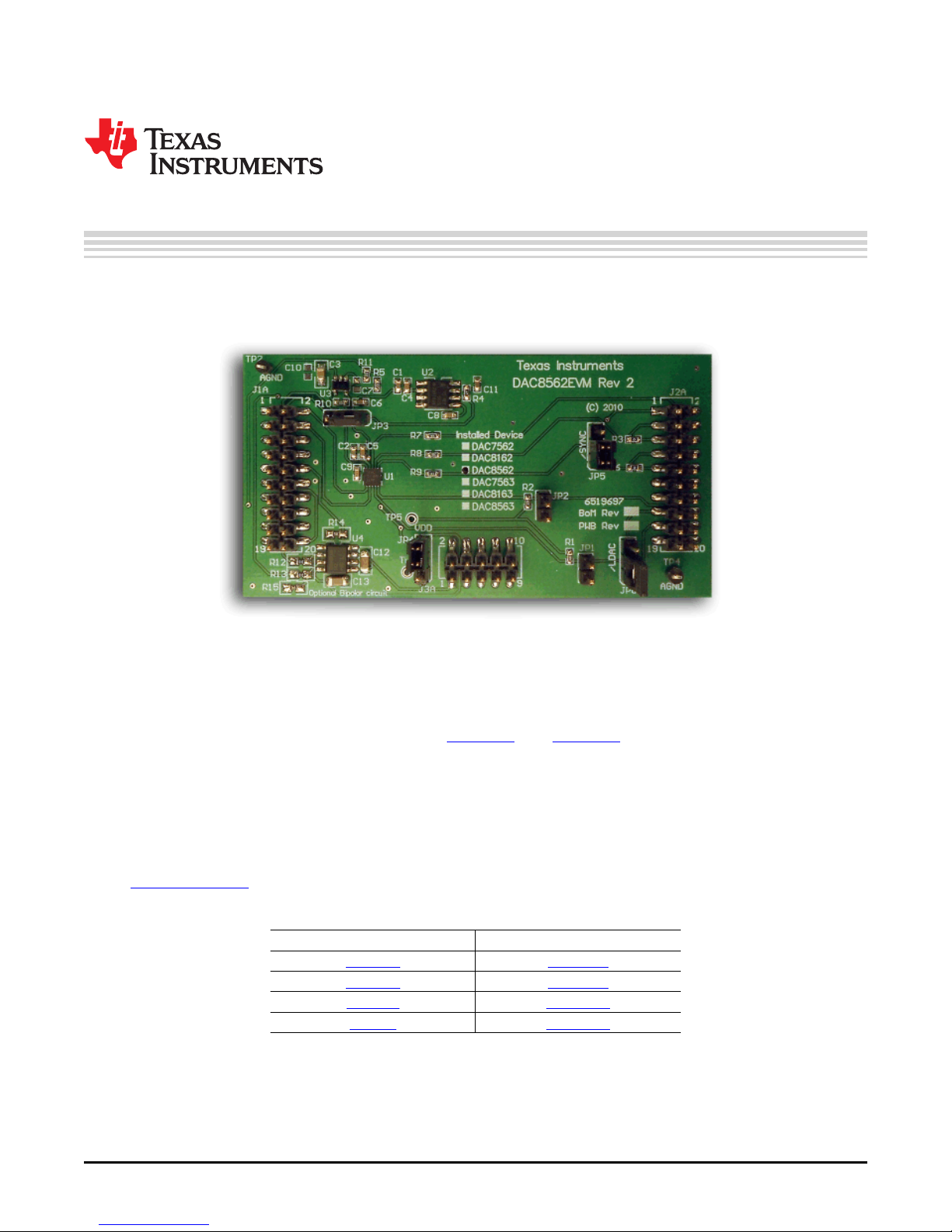
DAC7562EVM, DAC8562EVM
DAC8562EVM
This user's guide describes the characteristics, operation, and use of the DAC8562EVM. The evaluation
model (EVM) is an evaluation board for the DAC7562 and DAC8562. The DAC7562 and DAC8562 are
low-power, voltage-output, 12- or 16-bit digital-to-analog converters (DACs). These converters are
controlled through a serial peripheral interface (SPI) that can operate at clock rates of up to 50MHz.
Additionally, these DACs include a 2.5V internal reference voltage (disabled by default), giving a full-scale
output range of 5V when placed in a gain of two configuration. The EVM allows evaluation of all aspects of
the device and allows user control over every pin on the DAC7562/DAC8562. Complete circuit
descriptions, schematic diagrams, and bills of material are included in this document.
The following related documents are available for download through the Texas Instruments web site at
http://www.ti.com.
EVM-Related Device Data Sheets
Device Literature Number
DAC7562 SLAS719A
DAC8562 SLAS719A
REF5025 SBOS410D
OPA379 SBOS347D
All trademarks are the property of their respective owners.
SBAU183A–May 2011– Revised June 2011 DAC7562EVM, DAC8562EVM
Submit Documentation Feedback
1
Copyright © 2011, Texas Instruments Incorporated
Page 2

www.ti.com
Contents
1 EVM Overview ............................................................................................................... 3
2 Analog Interface ............................................................................................................. 3
3 Digital Interface .............................................................................................................. 4
4 Power Supplies .............................................................................................................. 5
5 Voltage Reference .......................................................................................................... 6
6 EVM Operation .............................................................................................................. 7
7 Schematics and Layout .................................................................................................... 9
List of Figures
1 Reference Selection Jumper JP3......................................................................................... 6
2 DAC8562EVM Default Jumper Locations ............................................................................... 8
3 DAC8562EVM: Top Layer Image ....................................................................................... 10
4 DAC8562EVM: Bottom Layer Image ................................................................................... 10
List of Tables
1 J1: Analog Interface Pinout................................................................................................ 3
2 J2.3: Serial Interface Pins.................................................................................................. 4
3 J3 Configuration: Power-Supply Input.................................................................................... 5
4 DAC8562EVM Jumpers.................................................................................................... 7
5 Bill of Materials ............................................................................................................. 9
2
DAC7562EVM, DAC8562EVM SBAU183A– May 2011– Revised June 2011
Copyright © 2011, Texas Instruments Incorporated
Submit Documentation Feedback
Page 3

www.ti.com
1 EVM Overview
1.1 Features
DAC8562EVM:
• Full-featured evaluation board for the DAC7562 or DAC8562
• Onboard optional external reference selection
• Wide selection of digital and I/O voltages
• Hardware or software control of control logic
• Compatible with the TI Modular EVM System
• Onboard optional bipolar circuit configuration (requires installing components)
This manual covers the operation of the DAC8562EVM. For simplicity, the DAC7562 and DAC8562 are
referred to as DACx562 throughout this document; unless otherwise noted, the information applies to
either DAC device. Additionally, the abbreviation EVM and the term evaluation module are synonymous
with the DAC8562EVM.
1.2 Introduction
The DACx562 series of devices are 10-pin, 12-, 14-, or 16-bit, low-power, two-channel digital-to-analog
converters (DACs) that operates from a single 2.7V to 5.5V supply. These DACs include a 2.5V internal
reference voltage (disabled by default), giving a full-scale output range of 5V when placed in a gain of two
configuration. The EVM is designed to highlight both the features of the small,10-pin QFN package that
the DACx562 is available in, and the performance of either the 12-bit or 16-bit DAC. Digital communication
is controlled through a three-wire SPI protocol allowing for speeds up to 50MHz.
The DAC8562EVM is designed to give the user access to all pins on the DACx562. The evaluation
module allows the user to control the DAC logic using onboard jumpers, or digitally through the J2 header.
By default, the evaluation module is configured to be used with an onboard 2.5V external reference, but
can be easily modified to use the DAC internal reference by changing a jumper setting and enabling the
internal reference using software.
The DAC8562EVM is an evaluation module built to the TI Modular EVM System specification. It can be
connected to any modular EVM system interface card. The DAC8562EVM does not have an onboard
microprocessor and cannot run software by itself. To connect it to a computer, some type of interface is
required.
EVM Overview
2 Analog Interface
For maximum flexibility, the DAC8562EVM can interface to multiple analog sources. Samtec part numbers
SSW-110-22-F-D-VS-K and TSM-110-01-T-DV-P provide a 10-pin, dual-row, header at J1. This header
provides access to the analog input and output pins of the DACx562. Consult Samtec at
http://www.samtec.com or call 1-800-SAMTEC-9 for a variety of mating connector options. Table 1
summarizes the pinouts for analog interface J1.
Pin Number Signal Description
J1.2 V
J1.4 V
J1.20 V
J1.1-1.13 (odd) GND Analog ground connection
J1.17-1.19 (odd) GND Analog ground connection
J1.6-1.18 (even) N/A —
J1.10 N/A
J1.12 - J1.18 (even) N/A —
J1.15 V
SBAU183A–May 2011– Revised June 2011 DAC7562EVM, DAC8562EVM
Submit Documentation Feedback
Table 1. J1: Analog Interface Pinout
-0 Analog output 0
OUT
-1 Analog output 1
OUT
REFIN/VREFOUT
Buf Buffered internal reference voltage
REF
Copyright © 2011, Texas Instruments Incorporated
External reference source input for
V
REFIN/VREFOUT
Op amp bipolar output (requires
installed components)
3
Page 4

Digital Interface
The analog interface is populated on both the top and the bottom sides of the evaluation board. All of the
output pins of the DACx562 are routed directly to the J1 connector.
The GND pins of the DACx562 are connected directly to the ground of the evaluation board.
The DAC8562EVM is designed to allow the user to choose from using the DACx562 internal reference,
the onboard 2.5V REF5025, or a user-supplied external reference source for the DAC. Depending on how
the DACx562 is configured, pin J1.20 is either an input or an output. If the DACx562 internal reference is
used, then J1.20 is the output of the V
than the onboard REF5025, J1.20 is used to provide the external reference voltage.
Additionally, the evaluation board contains an OPA379 in a buffer configuration to condition the internal
reference if the user would like to use the signal to drive another component. The buffered signal is routed
to pin J1.15.
If the DACx562 bipolar circuit is installed on the EVM, the output of the installed operational amplifier is
routed to pin J1.10 on the J1 connector.
3 Digital Interface
3.1 Serial Peripheral Interface
Samtec part numbers SSW-110-22-F-D-VS-K and TSM-110-01-T-DV-P provide a 10-pin, dual-row,
header/socket combination at J2. This header/socket provides access to the digital control data pins from
both J2A (top side) and J2B (bottom side) of the connector. Consult Samtec at http://www.samtec.com or
call 1-800-SAMTEC-9 for a variety of mating connector options. Table 2 describes the serial interface
pins.
REFIN/VREFOUT
www.ti.com
pin on the DAC. If an external reference is used, other
Table 2. J2.3: Serial Interface Pins
Pin No. Signal Name I/O Type Pull-Up Function
J2.1 SYNC0 In None DACx562 SYNC signal. Jumper
J2.3 SCLK In None DACx562 SCLK signal
J2.5 SCLK In None DACx562 SCLK signal
J2.7 SYNC1 In None DACx562 SYNC signal. Jumper
J2.9 SYNC2 In None DACx562 SYNC signal. Jumper
J2.11 SDI In None DACx562 DIN signal
J2.15 LDAC1 In High DACx562 LDAC signal. Jumper
J2.17 LDAC2 In High DACx562 LDAC signal. Jumper
J2.19 CLR In High DACx562 CLR signal.
J2.2 Unused — — —
J2.6 to J2.8 (even) Unused — — —
J2.12 to J2.16 (even) Unused — — —
J2.20 Unused — — —
J2.4, J2.10, J2.18 GND In/Out None Ground
JP5 determines SYNC pin
JP5 determines SYNC pin
JP5 determines SYNC pin
JP6 determines LDAC control pin
JP6 determines LDAC control pin
The DACx562 is controlled through a serial peripheral interface using the pins available on the J2 header.
The four SPI signals are connected to the DAC I/O signals through 33Ω series resistors. The SYNC signal
can be routed to one of three pins on the J2 header: J2.1, or J2.7 and J2.9. The SCLK signal is routed to
both J2.3 and J2.5. The DIN signal is routed to the J2.11 pin on the J2 header.
4
DAC7562EVM, DAC8562EVM SBAU183A– May 2011– Revised June 2011
Copyright © 2011, Texas Instruments Incorporated
Submit Documentation Feedback
Page 5

www.ti.com
There are two static I/O pins, LDAC and CLR, from the DACx562 that are routed to the J2 header. Both of
signals have weak pull-up resistors to the AVDD power-supply voltage. Either of these signals can be
pulled down using hardware jumpers or applying signals to the J2 header. Note that these signals are
edge-triggered.
The CLR pin is routed to pin J2.19. The LDAC pin is routed to either J2.15 or J2.17, selectable using the
JP6 onboard jumper. Updating the DACx562 output can be completed in one of three different ways. The
LDAC pin can be held low, and the output then update immediately following the last SCLK of the data
word. Alternatively, the LDAC can be held high, the DAC input register can be written to, and the output
then updates once the LDAC signal is brought low. A third technique is to overwrite the LDAC pin using
either register settings or DACx562 commands. See the product data sheet for more information.
4 Power Supplies
J3 is the power-supply input connector. Table 3 lists the configuration details for J3. The voltage inputs to
the DAC can be applied directly to the device. The DACx562 requires only one power supply to operate.
Pin No. Pin Name Function Required
J3.1 +VA +VA analog supply Optional
J3.2 –VA –VA analog supply Optional
J3.3 +5VA +5V analog supply Yes
J3.4 –5VA -5V analog supply No
J3.5 DGND Digital ground input Yes
J3.6 AGND Analog ground input Yes
J3.7 +1.8VD 1.8V digital supply No
J3.8 +3.3VD 3.3V digital supply No
J3.9 VD1 Not used No
J3.10 +5VD +5V No
Power Supplies
Table 3. J3 Configuration: Power-Supply Input
The digital and analog ground inputs are short-circuited internally through a ground plane.
The DAC8562EVM is designed to operate from a single +5V power supply (J3.3). This supply powers the
DACx562 itself, and the onboard REF5025 reference voltage source.
The DACx562 can be powered from a wide range of voltages from +2.7V to +5.5V. The onboard REF5025
is powered from the +5VA supply on the J3 header. Jumper JP4 is in place to allow users to choose
between the +5VA voltage to power the DAC or a separate, external power supply applied to TP1. This
flexibility allows the user to be able to properly power the REF5025 while powering the DAC from any
desired voltage within the specified range. The DAC8562EVM is not designed with any filters, so the use
of a clean, well-regulated supply is strongly recommended.
The +VA and –VA supplies are only used to power the optional external op amp, U4, and that is only if the
bipolar circuit is installed. Currently, the op amp is uninstalled and the EVM board does not require the
+VA and –VA supplies. If the op amp is installed, J3.1 and J3.2 must be powered by ±15V in order for the
bipolar circuit to be functional.
SBAU183A–May 2011– Revised June 2011 DAC7562EVM, DAC8562EVM
Submit Documentation Feedback
5
Copyright © 2011, Texas Instruments Incorporated
Page 6
Voltage Reference
5 Voltage Reference
The DAC8562EVM has a variety of reference voltage options. The 2.5V internal reference can be used;
the onboard REF5025 reference voltage can be used as an external source for the DAC; or the user can
input his own external reference voltage to the J1 header. Note that on the evaluation board, there is no
additional reference filtering or an op amp to drive the reference. This flexibility allows the user to have the
option to drive the reference directly with his own source.
The ability to have the DACx562 use its internal reference allows the V
either an input or an output. When the 2.5V internal reference voltage is used, the pin is an output. When
the DACx562 is configured to use an external reference voltage and the internal reference is disabled, the
pin is an input. Enabling and disabling the DACx562 internal reference is controlled internally through the
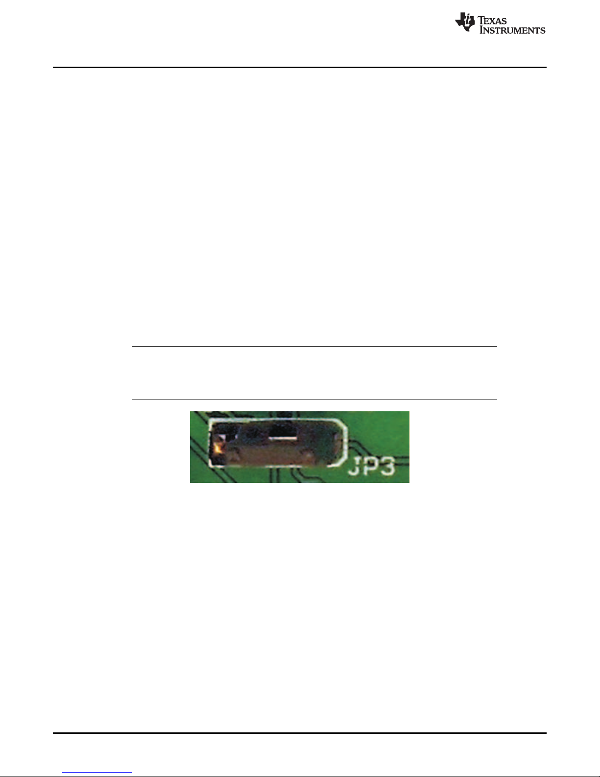
DAC registers and can be changed through the SPI communication protocol. Jumper JP3 must be set
accordingly, depending on the configuration of the reference voltage.
By default, the ability to have the DACx562 use its internal reference is disabled, and requires an external
reference voltage. Jumper JP3 controls which external reference source is used. When JP3 is in the 2-3
position (default), the REF5025 is used. When JP3 is in the 1-2 position, the user can input his own
reference voltage to analog header pin J1.20; this reference will then be routed to the DAC8562.
To enable the DACx562 internal reference voltage, make sure that jumper JP3 is either floating or
connected in the 1-2 position. This configuration avoids driving the V
reference voltage when the DACx562 has the V
conditioned through an onboard OPA379 before it is routed to pin J1.15 on the J1 header. This option
allows the user to drive external components without having to be concerned about the internal reference
source/sink capability.
REFIN/VREFOUT
www.ti.com
REFIN/VREFOUT
REFIN/VREFOUT
to be configured as
pin with the onboard
pin configured as an output. That signal is
NOTE: Do not place jumper JP3 in the 2-3 position while using the internal reference. If JP3 is in
the 2-3 position when the internal reference is used, the user will be attempting to drive the
V
REFIN/VREFOUT
condition may cause permanent damage to the DACx562.
pin externally while it is configured as the internal reference voltage output. This
Figure 1. Reference Selection Jumper JP3
6
DAC7562EVM, DAC8562EVM SBAU183A– May 2011– Revised June 2011
Copyright © 2011, Texas Instruments Incorporated
Submit Documentation Feedback
Page 7

www.ti.com
6 EVM Operation
This section provides information on the analog input, digital control, and general operating conditions of
the DAC8562EVM.
6.1 Analog Output
The DACx562 has two analog outputs that are available at the J1 header. Each of these outputs are
referenced to the board ground. Additionally, the J1 header is also used to either input an external
reference voltage, or read back the internal reference voltage of the DACx562. Depending on the JP3
configuration and the DACx562 internal reference status, the J1.19 pin may be used to input an external
source. The J1.15 pin is used to read back the DAC buffered internal reference when it is enabled.
The DAC8562EVM also has the option to install a bipolar circuit to evaluate using the DACx562 in bipolar
applications. After the necessary components are installed, the bipolar output from the external
operational amplifier is routed to J1.10.
6.2 Digital Control
The digital control signals can be applied directly to J2 (top or bottom side). The modular DAC8562EVM
can also be connected directly to a DSP or microcontroller interface board, such as the MMB0 DSP board
available from Texas Instruments.
No specific evaluation software is provided with this EVM. However, various code examples are available
that show how to use EVMs with a variety of digital signal processors from Texas Instruments. Check the
respective product folders on the TI web site or send an e-mail to dataconvapps@list.ti.com for a listing of
available code examples. The EVM Gerber files are available on request.
EVM Operation
6.3 Default Jumper Settings and Switch Positions
Table 4 lists the jumpers and the functionality of each that is available on the DAC8562EVM.
Table 4. DAC8562EVM Jumpers
Jumper Name Description
JP1 LDAC Control LDAC control pin; pulled high by default.
JP2 CLR Control CLR control pin; pulled high by default.
JP3 REF Selection DAC reference selection control
JP4 AVDD Selection AVDD selection control
JP5 SYNC Control Routes SYNC control to use either J2.1 or
JP6 LDAC Control Routes LDAC control to either J2.15 or
Apply shunt to tie pin to ground.
Apply shunt to tie pin to ground.
J2.7 and J2.9
J2.17
SBAU183A–May 2011– Revised June 2011 DAC7562EVM, DAC8562EVM
Submit Documentation Feedback
7
Copyright © 2011, Texas Instruments Incorporated
Page 8

EVM Operation
Figure 2 shows the default jumper conditions for the DAC8562EVM.
www.ti.com
Figure 2. DAC8562EVM Default Jumper Locations
The DAC8562EVM board has six onboard hardware jumpers that are used to control the power options
and digital I/O signals. Two position jumpers, JP1 and JP2, are used to control whether to pull the LDAC
and CLR signals high or low. Leave the jumpers open to pull the corresponding signal high, or apply a
shunt across the jumper to tie the signal low.
JP3 routes where the V
REFIN/VREFOUT
I/O pin on the DACx562 is routed. When JP3 is in its default position,
the shunt is placed across pins JP3.2 and JP3.3. This configuration allows the DACx562 to use the
onboard REF5025 as the external reference. When JP3 is in the 1-2 position, the user can input an
external reference voltage to analog header pin J1.20, which is then routed to the DAC. If the DACx562
internal reference is enabled, the user must ensure that jumper JP3 is either floating or connected in the
1-2 position. The internal reference voltage is then buffered through the OPA379 and routed to J1.20. It is
important to not have jumper JP3 in the 2-3 position while using the internal reference. You cannot drive
the V
REFIN/VREFOUT
pin externally while it is configured as the internal reference voltage output. Doing so
may permanently damage the DAC8562.
The DAC AVDDpower source is controlled by jumper JP4. By default, AVDDis powered from J3.3 (JP4
position 1-2). It can also be powered from TP1 if the shunt is placed across pins 2-3.
The SYNC signal can either be routed to the J2.1 pin or the J2.7 and J2.9 pins. This routing option is
controlled using the JP5 jumper.
Jumper JP6 selects where to route the LDAC signal. By default, pins JP6.2 and JP6.3 are connected to
route the LDAC signal to J2.17. The shunt can be placed across JP6.1 and JP6.2 to route the LDAC
signal to J2.15.
8
DAC7562EVM, DAC8562EVM SBAU183A– May 2011– Revised June 2011
Copyright © 2011, Texas Instruments Incorporated
Submit Documentation Feedback
Page 9

www.ti.com
Schematics and Layout
7 Schematics and Layout
Schematics for the DAC8562EVM are appended to this user's guide. Figure 3 and Figure 4 are the printed
circuit board (PCB) layouts. The bill of materials is provided in Table 5.
7.1 Bill of Materials
NOTE: All components should be compliant with the European Union Restriction on Use of
Hazardous Substances (RoHS) Directive. Some part numbers may be either leaded or
RoHS. Verify that purchased components are RoHS-compliant. (For more information about
TI's position on RoHS compliance, see the Quality and Eco-Info information on the TI web
site.)
Table 5. Bill of Materials
Item No. Qty Ref Des Description Vendor Part Number
1 3 C1, C2, C11 Capacitor, ceramic, 10μF, 6.3V X5R 0603 Murata GRM188R60J106ME47D
2 1 C3 Capacitor, ceramic, 22μF, 6.3V 20% X5R Murata GRM21BR60J226ME39L
3 3 C4, C5, C6 Capacitor, ceramic, 0.1μF, 16V 10% X7R Murata GRM188R71C104KA01D
4 4 C7, C10, C12, C13 Not installed — —
5 1 C8 Capacitor, ceramic, 1.0μF, 16V 10% X5R Murata GRM188R61C105KA93D
6 1 C9 Capacitor, ceramic, 2.2μF, 10V 20% X5R Murata GRM188R61A225ME34D
7 2 J1A, J2A (Top Side) 10-pin, dual row, SM header (20 Pos.) Samtec TSM-110-01-T-DV-P
8 2 J1B, J2B (Bottom Side) 10-pin, dual row, SM header (20 Pos.) Samtec SSW-110-22-F-D-VS-K
9 1 J3A (Top Side) 5-pin, dual row, SM header (10 Pos.) Samtec TSM-105-01-T-DV-P
10 1 J3B (Bottom Side) 5-pin, dual row, SM header (10 Pos.) Samtec SSW-105-22-F-D-VS-K
11 2 JP1, JP2 Header strip, 2 pin (1x2) Samtec TSW-102-07-L-S
12 4 JP3, JP4, JP5, JP6 Header strip, 3 pin (1x3) Samtec TSW-103-07-L-S
13 3 R1, R2, R10 Resistor, 10kΩ 1/10W 5% 0603 SMD Panasonic ERJ-3GEYJ103V
14 2 R3, R6 Resistor, 0Ω 1/10W 5% 0603 SMD Panasonic ERJ-3GEY0R00V
15 1 R4 Resistor, 0.47Ω 1/10W 5% 0603 Panasonic ERJ-3RQJR47V
16 1 R5 Resistor, 2.0kΩ 1/10W 5% 0603 SMD Panasonic ERJ-3GEYJ202V
17 4 R7, R8, R9, R11 Resistor, 33Ω 1/10W 5% 0603 SMD Panasonic ERJ-3GEYJ330V
18 4 R12, R13, R14, R15 Not installed — —
19 3 TP1, TP3, TP5 Test Point, Single .025 pin, red Keystone 5000
20 2 TP2, TP4 Test Point, Single .025 pin, black Keystone 5001
21 1 U1 Texas Instruments
22 1 U2 Precision voltage reference 2.5V, 8-SOIC Texas Instruments REF5025ID
23 1 U3 IC Op Amp GP R-R 90kHz, SOT23-5 Texas Instruments OPA379AIDBVT
24 1 U4 Not installed — —
25 7 N/A 0.100 Shunt, black Samtec SNT-100-BK-T
(1)
The device installed at location U1 depends on the EVM purchased.
0805
0603
0603
0603
12-bit, dual-channel, high-precision DAC,
10-pin QFN
16-bit, dual-channel, high-precision DAC,
10-pin QFN
DAC7562SDSC or
DAC8562SDSC
(1)
SBAU183A–May 2011– Revised June 2011 DAC7562EVM, DAC8562EVM
Submit Documentation Feedback
9
Copyright © 2011, Texas Instruments Incorporated
Page 10

Schematics and Layout
www.ti.com
Figure 3. DAC8562EVM: Top Layer Image
Figure 4. DAC8562EVM: Bottom Layer Image
10
DAC7562EVM, DAC8562EVM SBAU183A– May 2011– Revised June 2011
Copyright © 2011, Texas Instruments Incorporated
Submit Documentation Feedback
Page 11

www.ti.com
Revision History
Revision History
Changes from Original (May, 2011) to A Revision .......................................................................................................... Page
• Updated document title to reflect DAC7562EVM device ............................................................................ 1
NOTE: Page numbers for previous revisions may differ from page numbers in the current version.
SBAU183A–May 2011– Revised June 2011 Revision History
Submit Documentation Feedback
11
Copyright © 2011, Texas Instruments Incorporated
Page 12

A
B
C
D
D
C
B
A
ti
12500 TI Boulevard. Dallas, Texas 75243
Title:
SHEET: OF:
FILE: SIZE:
DATE:
REV:
20-Dec-2010
Drawn By:
Engineer:
Revision History
REV ECN Number Approved
DAC8562_R1.Sch
DOCUMENTCONTROL #
DAC8562 EVM
A
1
2 Second Proto Release
1
+5VA
SCLK
SDI
VDD
-VA
2
-5VA
4
AGND
6
VD1
8
+5VD
10
+VA
1
+5VA
3
DGND
5
+1.8VD
7
+3.3VD
9
J3A
DAUGHTER-POWER
A0(+)
2
A1(+)
4
A2(+)
6
A3(+)
8
A4
10
A5
12
A6
14
A7
16
REF-
18
REF+
20
A0(-)
1
A1(-)
3
A2(-)
5
A3(-)
7
AGND
9
AGND
11
AGND
13
VCOM
15
AGND
17
AGND
19
J1A
OUTPUT HEADER
GPIO0
2
DGND
4
GPIO1
6
GPIO2
8
DGND
10
GPIO3
12
GPIO4
14
SCL
16
DGND
18
SDA
20
CNTL
1
CLKX
3
CLKR
5
FSX
7
FSR
9
DX
11
DR
13
INT
15
TOUT
17
GPIO5
19
J2A
DAUGHTER-SERIAL
R1
10KR210K
C5
0.1uF
C2
10uF
JP4
R6 0
R8 33
JP2
JP1
VIN2VOUT
6
TRIM
5
GND
4
TEMP
3
U2
REF5025ID
C1
10uFC40.1uF
R7 33
C6
0.1uF
C8
1uF
C7 NI
C10
NI
C9
2.2uF
TP1
TP4
TP2
Production Release
JP5
/SYNC
OUT_B
OUT_A
SYNC1
SYNC0
VDD
R4
0.47
R5
2K
3
4
1
2 5
U3
OPA379
JP6
C3
22uF
JP3
/CLR
/LDAC
R11
33
C11
10uF
/CLR
/LDAC
R3 0
R10
10K
VDD
VDD
VDD
TP5
A
VoutA
1
/SYNC
6
DIN
8
/CLR
5
/LDAC
4
AVdd
9
VoutB
2
GND
3
SCLK
7
REFin/out
10
U1
DAC8562DSC
R9 33
SYNC2
R12
DNI
R14
DNI
R13
DNI
R15
DNI
2
3
6
74
U4
DNI
C12
DNI
C13
DNI
Optional circuit to create Bipolar output
+VA
-VA
+VA -VA
Page 13

Evaluation Board/Kit Important Notice
Texas Instruments (TI) provides the enclosed product(s) under the following conditions:
This evaluation board/kit is intended for use for ENGINEERING DEVELOPMENT, DEMONSTRATION, OR EVALUATION
PURPOSES ONLY and is not considered by TI to be a finished end-product fit for general consumer use. Persons handling the
product(s) must have electronics training and observe good engineering practice standards. As such, the goods being provided are
not intended to be complete in terms of required design-, marketing-, and/or manufacturing-related protective considerations,
including product safety and environmental measures typically found in end products that incorporate such semiconductor
components or circuit boards. This evaluation board/kit does not fall within the scope of the European Union directives regarding
electromagnetic compatibility, restricted substances (RoHS), recycling (WEEE), FCC, CE or UL, and therefore may not meet the
technical requirements of these directives or other related directives.
Should this evaluation board/kit not meet the specifications indicated in the User’s Guide, the board/kit may be returned within 30
days from the date of delivery for a full refund. THE FOREGOING WARRANTY IS THE EXCLUSIVE WARRANTY MADE BY
SELLER TO BUYER AND IS IN LIEU OF ALL OTHER WARRANTIES, EXPRESSED, IMPLIED, OR STATUTORY, INCLUDING
ANY WARRANTY OF MERCHANTABILITY OR FITNESS FOR ANY PARTICULAR PURPOSE.
The user assumes all responsibility and liability for proper and safe handling of the goods. Further, the user indemnifies TI from all
claims arising from the handling or use of the goods. Due to the open construction of the product, it is the user’s responsibility to
take any and all appropriate precautions with regard to electrostatic discharge.
EXCEPT TO THE EXTENT OF THE INDEMNITY SET FORTH ABOVE, NEITHER PARTY SHALL BE LIABLE TO THE OTHER
FOR ANY INDIRECT, SPECIAL, INCIDENTAL, OR CONSEQUENTIAL DAMAGES.
TI currently deals with a variety of customers for products, and therefore our arrangement with the user is not exclusive.
TI assumes no liability for applications assistance, customer product design, software performance, or infringement of
patents or services described herein.
Please read the User’s Guide and, specifically, the Warnings and Restrictions notice in the User’s Guide prior to handling the
product. This notice contains important safety information about temperatures and voltages. For additional information on TI’s
environmental and/or safety programs, please contact the TI application engineer or visit www.ti.com/esh.
No license is granted under any patent right or other intellectual property right of TI covering or relating to any machine, process, or
combination in which such TI products or services might be or are used.
FCC Warning
This evaluation board/kit is intended for use for ENGINEERING DEVELOPMENT, DEMONSTRATION, OR EVALUATION
PURPOSES ONLY and is not considered by TI to be a finished end-product fit for general consumer use. It generates, uses, and
can radiate radio frequency energy and has not been tested for compliance with the limits of computing devices pursuant to part 15
of FCC rules, which are designed to provide reasonable protection against radio frequency interference. Operation of this
equipment in other environments may cause interference with radio communications, in which case the user at his own expense
will be required to take whatever measures may be required to correct this interference.
EVM Warnings and Restrictions
It is important to operate this EVM within the input voltage range of 0V to 5.5V and the output voltage range of 0V to 5.5V.
Exceeding the specified input range may cause unexpected operation and/or irreversible damage to the EVM. If there are
questions concerning the input range, please contact a TI field representative prior to connecting the input power.
Applying loads outside of the specified output range may result in unintended operation and/or possible permanent damage to the
EVM. Please consult the EVM User's Guide prior to connecting any load to the EVM output. If there is uncertainty as to the load
specification, please contact a TI field representative.
During normal operation, some circuit components may have case temperatures greater than +30°C. The EVM is designed to
operate properly with certain components above +85°C as long as the input and output ranges are maintained. These components
include but are not limited to linear regulators, switching transistors, pass transistors, and current sense resistors. These types of
devices can be identified using the EVM schematic located in the EVM User's Guide. When placing measurement probes near
these devices during operation, please be aware that these devices may be very warm to the touch.
Mailing Address: Texas Instruments, Post Office Box 655303, Dallas, Texas 75265
Copyright © 2011, Texas Instruments Incorporated
Page 14

IMPORTANT NOTICE
Texas Instruments Incorporated and its subsidiaries (TI) reserve the right to make corrections, modifications, enhancements, improvements,
and other changes to its products and services at any time and to discontinue any product or service without notice. Customers should
obtain the latest relevant information before placing orders and should verify that such information is current and complete. All products are
sold subject to TI’s terms and conditions of sale supplied at the time of order acknowledgment.
TI warrants performance of its hardware products to the specifications applicable at the time of sale in accordance with TI’s standard
warranty. Testing and other quality control techniques are used to the extent TI deems necessary to support this warranty. Except where
mandated by government requirements, testing of all parameters of each product is not necessarily performed.
TI assumes no liability for applications assistance or customer product design. Customers are responsible for their products and
applications using TI components. To minimize the risks associated with customer products and applications, customers should provide
adequate design and operating safeguards.
TI does not warrant or represent that any license, either express or implied, is granted under any TI patent right, copyright, mask work right,
or other TI intellectual property right relating to any combination, machine, or process in which TI products or services are used. Information
published by TI regarding third-party products or services does not constitute a license from TI to use such products or services or a
warranty or endorsement thereof. Use of such information may require a license from a third party under the patents or other intellectual
property of the third party, or a license from TI under the patents or other intellectual property of TI.
Reproduction of TI information in TI data books or data sheets is permissible only if reproduction is without alteration and is accompanied
by all associated warranties, conditions, limitations, and notices. Reproduction of this information with alteration is an unfair and deceptive
business practice. TI is not responsible or liable for such altered documentation. Information of third parties may be subject to additional
restrictions.
Resale of TI products or services with statements different from or beyond the parameters stated by TI for that product or service voids all
express and any implied warranties for the associated TI product or service and is an unfair and deceptive business practice. TI is not
responsible or liable for any such statements.
TI products are not authorized for use in safety-critical applications (such as life support) where a failure of the TI product would reasonably
be expected to cause severe personal injury or death, unless officers of the parties have executed an agreement specifically governing
such use. Buyers represent that they have all necessary expertise in the safety and regulatory ramifications of their applications, and
acknowledge and agree that they are solely responsible for all legal, regulatory and safety-related requirements concerning their products
and any use of TI products in such safety-critical applications, notwithstanding any applications-related information or support that may be
provided by TI. Further, Buyers must fully indemnify TI and its representatives against any damages arising out of the use of TI products in
such safety-critical applications.
TI products are neither designed nor intended for use in military/aerospace applications or environments unless the TI products are
specifically designated by TI as military-grade or "enhanced plastic." Only products designated by TI as military-grade meet military
specifications. Buyers acknowledge and agree that any such use of TI products which TI has not designated as military-grade is solely at
the Buyer's risk, and that they are solely responsible for compliance with all legal and regulatory requirements in connection with such use.
TI products are neither designed nor intended for use in automotive applications or environments unless the specific TI products are
designated by TI as compliant with ISO/TS 16949 requirements. Buyers acknowledge and agree that, if they use any non-designated
products in automotive applications, TI will not be responsible for any failure to meet such requirements.
Following are URLs where you can obtain information on other Texas Instruments products and application solutions:
Products Applications
Audio www.ti.com/audio Communications and Telecom www.ti.com/communications
Amplifiers amplifier.ti.com Computers and Peripherals www.ti.com/computers
Data Converters dataconverter.ti.com Consumer Electronics www.ti.com/consumer-apps
DLP® Products www.dlp.com Energy and Lighting www.ti.com/energy
DSP dsp.ti.com Industrial www.ti.com/industrial
Clocks and Timers www.ti.com/clocks Medical www.ti.com/medical
Interface interface.ti.com Security www.ti.com/security
Logic logic.ti.com Space, Avionics and Defense www.ti.com/space-avionics-defense
Power Mgmt power.ti.com Transportation and www.ti.com/automotive
Microcontrollers microcontroller.ti.com Video and Imaging www.ti.com/video
RFID www.ti-rfid.com Wireless www.ti.com/wireless-apps
RF/IF and ZigBee® Solutions www.ti.com/lprf
TI E2E Community Home Page e2e.ti.com
Automotive
Mailing Address: Texas Instruments, Post Office Box 655303, Dallas, Texas 75265
Copyright © 2011, Texas Instruments Incorporated
 Loading...