

Page 1
DAC756x
DAC816x
DAC856x
(12-Bit)
(14-Bit)
(16-Bit)
Data Buffer A
DAC Register A
Buffer Control Register Control
Control Logic
Power-
Down
Control
Logic
AV
DD
V
REFIN REFOUT
/V
CLRLDAC
2.5-V
Reference
Data Buffer B
DAC Register B
V B
OUT
V A
OUT
GND
DAC
DAC
Input Control Logic
SYNC
SCLK
D
IN
DAC8562, DAC8563
DAC8162, DAC8163
DAC7562, DAC7563
www.ti.com
SLAS719C –AUGUST 2010– REVISED JUNE 2011
DUAL 16-/14-/12-BIT, ULTRALOW-GLITCH, LOW-POWER, BUFFERED, VOLTAGE-OUTPUT
DAC WITH 2.5-V, 4-PPM/°C INTERNAL REFERENCE IN SMALL 3-MM × 3-MM QFN
Check for Samples: DAC8562, DAC8563, DAC8162, DAC8163, DAC7562, DAC7563
1
FEATURES
23
• Relative Accuracy:
– DAC856x (16-Bit): 4 LSB INL
– DAC816x (14-Bit): 1 LSB INL
– DAC756x (12-Bit): 0.3 LSB INL
• Glitch Energy: 0.1 nV-s
• Bidirectional Reference: Input or 2.5-V Output
– Output Disabled by Default
– ±5-mV Initial Accuracy (Max)
– 4-ppm/°C Temperature Drift (Typ)
– 10-ppm/°C Temperature Drift (Max)
– 20-mA Sink/Source Capability
• Power-On Reset to Zero Scale or Mid-Scale
• Low-Power: 4 mW (Typ, 5-V AVDD, Including
Internal Reference Current)
• Wide Power-Supply Range: 2.7 V to 5.5 V
• 50-MHz SPI With Schmitt-Triggered Inputs
• LDAC and CLR Functions
• Output Buffer With Rail-to-Rail Operation
• Packages: QFN-10 (3x3 mm), MSOP-10
• Temperature Range: –40°C to 125°C
APPLICATIONS
• Portable Instrumentation
• Bipolar Outputs (reference design)
• PLC Analog Output Module (reference design)
• Closed-Loop Servo Control
• Voltage Controlled Oscillator Tuning
• Data Acquisition Systems
• Programmable Gain and Offset Adjustment
DESCRIPTION
The DAC856x, DAC816x, and DAC756x are
low-power, voltage-output, dual-channel, 16-, 14-,
and 12-bit digital-to-analog converters (DACs),
respectively. These devices include a 2.5-V,
4-ppm/°C internal reference, giving a full-scale output
voltage range of 2.5 V or 5 V. The internal reference
has an initial accuracy of ±5 mV and can source or
sink up to 20 mA at the V
REFIN/VREFOUT
These devices are monotonic, providing excellent
linearity and minimizing undesired code-to-code
transient voltages (glitch). They use a versatile
three-wire serial interface that operates at clock rates
up to 50 MHz. The interface is compatible with
standard SPI™, QSPI™, Microwire™, and digital
signal processor (DSP) interfaces. The DACxx62
devices incorporate a power-on-reset circuit that
ensures the DAC output powers up at zero scale until
a valid code is written to the device, whereas the
DACxx63s similarly power up at mid-scale. These
devices contain a power-down feature that reduces
current consumption to typically 10 nA at 5 V. The
low power consumption, internal reference, and small
footprint make these devices ideal for portable,
battery-operated equipment.
The DACxx62 devices are drop-in and
function-compatible with each other, as are the
DACxx63s. The entire family is available in MSOP-10
and QFN-10 packages.
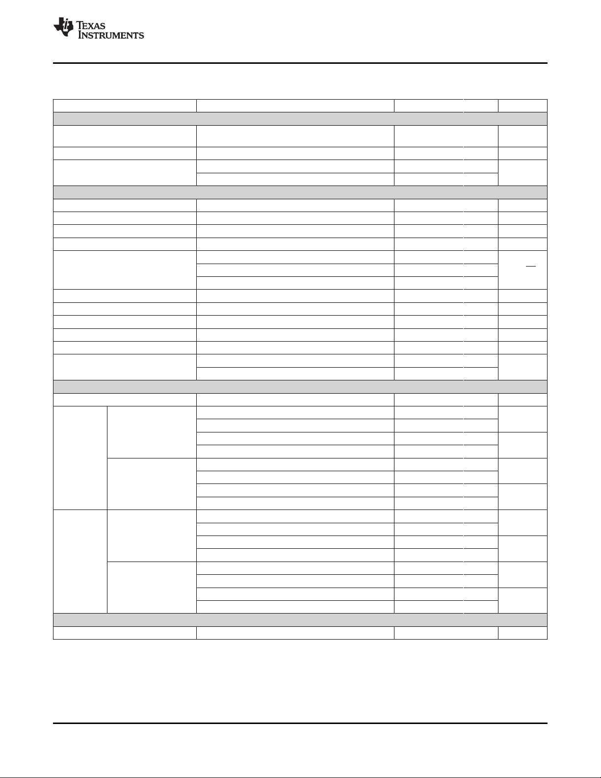
Table 1. RELATED DEVICES
16-BIT 14-BIT 12-BIT
Reset to zero DAC8562 DAC8162 DAC7562
Reset to mid-scale DAC8563 DAC8163 DAC7563
pin.
1
2SPI, QSPI are trademarks of Motorola, Inc.
3Microwire is a trademark of National Semiconductor.
PRODUCTION DATA information is current as of publication date.
Products conform to specifications per the terms of the Texas
Instruments standard warranty. Production processing does not
necessarily include testing of all parameters.
Please be aware that an important notice concerning availability, standard warranty, and use in critical applications of Texas
Instruments semiconductor products and disclaimers thereto appears at the end of this data sheet.
Copyright © 2010–2011, Texas Instruments Incorporated
Page 2
DAC8562, DAC8563
DAC8162, DAC8163
DAC7562, DAC7563
SLAS719C –AUGUST 2010– REVISED JUNE 2011
This integrated circuit can be damaged by ESD. Texas Instruments recommends that all integrated circuits be handled with
appropriate precautions. Failure to observe proper handling and installation procedures can cause damage.
ESD damage can range from subtle performance degradation to complete device failure. Precision integrated circuits may be more
susceptible to damage because very small parametric changes could cause the device not to meet its published specifications.
www.ti.com
DEVICE INFORMATION
MAXIMUM MAXIMUM MAXIMUM
PRODUCT TEMPER-
DAC8562 Zero 8562
DAC8563 Mid-scale 8563
DAC8162 Zero 8162
DAC8163 Mid-scale 8163
DAC7562 Zero 7562
DAC7563 Mid-scale 7563
RELATIVE DIFFERENTIAL REFERENCE RESET PACKAGE- PACKAGE PACKAGE
ACCURACY NONLINEARITY DRIFT TO LEAD DESIGNATOR MARKING
(LSB) (LSB) (ppm/°C)
±12 ±1 10 –40°C to 125°C
±3 ±0.5 10 –40°C to 125°C
±0.75 ±0.25 10 –40°C to 125°C
(1)
SPECIFIED
ATURE RANGE
QFN-10 DSC
MSOP-10 DGS
QFN-10 DSC
MSOP-10 DGS
QFN-10 DSC
MSOP-10 DGS
QFN-10 DSC
MSOP-10 DGS
QFN-10 DSC
MSOP-10 DGS
QFN-10 DSC
MSOP-10 DGS
(1) For the most current package and ordering information, see the Package Option Addendum at the end of this data sheet, or see the TI
Web site at www.ti.com.
2 Copyright © 2010–2011, Texas Instruments Incorporated
Page 3
DAC8562, DAC8563
DAC8162, DAC8163
DAC7562, DAC7563
www.ti.com
ABSOLUTE MAXIMUM RATINGS
(1)
Over operating free-air temperature range (unless otherwise noted).
AVDDto GND –0.3 to 6 V
CLR, DIN, LDAC, SCLK and SYNC input voltage to GND –0.3 to AVDD+ 0.3 V
V
to GND –0.3 to AVDD+ 0.3 V
OUT
V
REFIN/VREFOUT
to GND –0.3 to AVDD+ 0.3 V
Operating temperature range –40 to 125 °C
Junction temperature, maximum (T
) 150 °C
J max
(1) Stresses beyond those listed under Absolute Maximum Ratings may cause permanent damage to the device. These are stress ratings
only, and functional operation of the device at these or any other conditions beyond those indicated under Recommended Operating
Conditions is not implied. Exposure to absolute-maximum-rated conditions for extended periods may affect device reliability.
THERMAL INFORMATION
THERMAL METRIC DSC DGS UNIT
θ
θ
θ
ψ
ψ
θ
JA
JCtop
JB
JT
JB
JCbot
Junction-to-ambient thermal resistance
Junction-to-case (top) thermal resistance
Junction-to-board thermal resistance
Junction-to-top characterization parameter
Junction-to-board characterization parameter
Junction-to-case (bottom) thermal resistance
(1) The junction-to-ambient thermal resistance under natural convection is obtained in a simulation on a JEDEC-standard, high-K board, as
specified in JESD51-7, in an environment described in JESD51-2a.
(2) The junction-to-case (top) thermal resistance is obtained by simulating a cold plate test on the package top. No specific
JEDEC-standard test exists, but a close description can be found in the ANSI SEMI standard G30-88.
(3) The junction-to-board thermal resistance is obtained by simulating in an environment with a ring cold plate fixture to control the PCB
temperature, as described in JESD51-8.
(4) The junction-to-top characterization parameter, ψJT, estimates the junction temperature of a device in a real system and is extracted
from the simulation data for obtaining θJA, using a procedure described in JESD51-2a (sections 6 and 7).
(5) The junction-to-board characterization parameter, ψJB, estimates the junction temperature of a device in a real system and is extracted
from the simulation data for obtaining θJA, using a procedure described in JESD51-2a (sections 6 and 7).
(6) The junction-to-case (bottom) thermal resistance is obtained by simulating a cold plate test on the exposed (power) pad. No specific
JEDEC standard test exists, but a close description can be found in the ANSI SEMI standard G30-88.
(1)
(2)
(3)
(4)
(5)
(6)
SLAS719C –AUGUST 2010– REVISED JUNE 2011
VALUE UNIT
DAC856x, DAC816x, DAC756x
10 PINS 10 PINS
62.8 173.8 °C/W
44.3 48.5 °C/W
26.5 79.9 °C/W
0.4 1.7 °C/W
25.5 68.4 °C/W
46.2 N/A °C/W
Copyright © 2010–2011, Texas Instruments Incorporated Submit Documentation Feedback 3
Product Folder Link(s): DAC8562 DAC8563 DAC8162 DAC8163 DAC7562 DAC7563
Page 4
DAC8562, DAC8563
DAC8162, DAC8163
DAC7562, DAC7563
SLAS719C –AUGUST 2010– REVISED JUNE 2011
ELECTRICAL CHARACTERISTICS
At AVDD= 2.7 V to 5.5 V and TA= –40°C to 125°C (unless otherwise noted).
PARAMETER TEST CONDITIONS MIN TYP MAX UNIT
STATIC PERFORMANCE
Resolution 16 Bits
DAC856x Relative accuracy Using line passing through codes 512 and 65,024 ±4 ±12 LSB
Differential nonlinearity 16-bit monotonic ±0.2 ±1 LSB
Resolution 14 Bits
DAC816x Relative accuracy Using line passing through codes 128 and 16,256 ±1 ±3 LSB
Differential nonlinearity 14-bit monotonic ±0.1 ±0.5 LSB
Resolution 12 Bits
DAC756x Relative accuracy Using line passing through codes 32 and 4,064 ±0.3 ±0.75 LSB
Differential nonlinearity 12-bit monotonic ±0.05 ±0.25 LSB
Offset error Extrapolated from two-point line
Offset error drift ±2 µV/°C
Full-scale error DAC register loaded with all 1s ±0.03 ±0.2 % FSR
Zero-code error DAC register loaded with all 0s 1 4 mV
Zero-code error drift ±2 µV/°C
Gain error Extrapolated from two-point line
Gain temperature coefficient ±1
OUTPUT CHARACTERISTICS
Output voltage range 0 AV
Output voltage settling time
Slew rate Measured between 20% - 80% of a full-scale transition 0.75 V/µs
Capacitive load stability nF
Code-change glitch impulse 1-LSB change around major carry 0.1 nV-s
Digital feedthrough SCLK toggling, SYNC high 0.1 nV-s
Power-on glitch impulse RL= 2 kΩ, CL= 470 pF, AVDD= 5.5 V 40 mV
Channel-to-channel dc crosstalk µV
DC output impedance At mid-scale input 5 Ω
Short-circuit current 40 mA
Power-up time, including settling time Coming out of power-down mode 50 µs
AC PERFORMANCE
DAC output noise density TA= 25°C, at mid-scale input, f
DAC output noise TA= 25°C, at mid-scale input, 0.1 Hz to 10 Hz 2.6 µV
LOGIC INPUTS
(2)
Input pin Leakage current –1 ±0.1 1 µA
Logic input LOW voltage VINL 0 0.8 V
Logic input HIGH voltage VINH AV
Pin capacitance 3 pF
(1) 16-bit: codes 512 and 65,024; 14-bit: codes 128 and 16,256; 12-bit: codes 32 and 4,064
(2) Specified by design or characterization
(3) Transition time between 1/4 scale and 3/4 scale including settling to within ±0.024% FSR
(1)
(1)
, unloaded ±1 ±4 mV
(1)
, unloaded ±0.01 ±0.15 % FSR
(2)
(3)
DACs unloaded 7
RL= 1 MΩ 10
RL= ∞ 1
RL= 2 kΩ 3
Full-scale swing on adjacent channel,
External reference
Full-scale swing on adjacent channel,
Internal reference
5
15
DAC outputs at full-scale, DAC outputs shorted to
GND
(2)
= 1 kHz 90 nV/√Hz
OUT
0.7 ×
AV
DD
DD
DD
www.ti.com
ppm
FSR/°C
V
µs
V
PP
4 Submit Documentation Feedback Copyright © 2010–2011, Texas Instruments Incorporated
Product Folder Link(s): DAC8562 DAC8563 DAC8162 DAC8163 DAC7562 DAC7563
Page 5
DAC8562, DAC8563
DAC8162, DAC8163
DAC7562, DAC7563
www.ti.com
ELECTRICAL CHARACTERISTICS (continued)
At AVDD= 2.7 V to 5.5 V and TA= –40°C to 125°C (unless otherwise noted).
PARAMETER TEST CONDITIONS MIN TYP MAX UNIT
REFERENCE
External reference current 15 µA
V
reference input range 0 AV
REFIN
Reference input impedance kΩ
External V
disabled), all channels active using gain = 1
Internal reference disabled, gain = 1 170
Internal reference disabled, gain = 2 85
REFERENCE OUTPUT
Output voltage TA= 25°C 2.495 2.5 2.505 V
Initial accuracy TA= 25°C –5 ±0.1 5 mV
Output voltage temperature drift
(4)
Output voltage noise f = 0.1 Hz to 10 Hz 12 µV
TA= 25°C, f = 1 kHz, CL= 0 µF 250
Output voltage noise density
(high-frequency noise)
TA= 25°C, f = 1 MHz, CL= 0 µF 30 nV/√Hz
TA= 25°C, f = 1 MHz, CL= 4.7 µF 10
Load regulation, sourcing
Load regulation, sinking
Output current load capability
(5)
(5)
(6)
TA= 25°C 20 µV/mA
TA= 25°C 185 µV/mA
Line regulation TA= 25°C 50 µV/V
Long-term stability/drift (aging)
Thermal hysteresis
(5)
POWER REQUIREMENTS
(5)
TA= 25°C, time = 0 to 1900 hours 100 ppm
First cycle 200
Additional cycles 50
(7)
Power supply voltage 2.7 5.5 V
Normal mode, internal reference off 0.25 0.5
AVDD= 3.6 V to 5.5 V
I
DD
AVDD= 2.7 V to 3.6 V
Normal mode, internal reference on 0.8 1.3
Power-down modes
Power-down modes
Normal mode, internal reference off 0.2 0.4
Normal mode, internal reference on 0.73 1.3
Power-down modes
Power-down modes
Normal mode, internal reference off 0.9 2.75
AVDD= 3.6 V to 5.5 V
Power
dissipation
AVDD= 2.7 V to 3.6 V
Normal mode, internal reference on 2.9 7.15
Power-down modes
Power-down modes
Normal mode, internal reference off 0.54 1.44
Normal mode, internal reference on 1.97 4.68
Power-down modes
Power-down modes
TEMPERATURE RANGE
Specified performance –40 125 °C
(4) Internal reference output voltage temperature drift is characterized from –40°C to 125°C.
(5) Explained in more detail in the Application Information section of this data sheet.
(6) Specified by design or characterization
(7) Input code = mid-scale, no load, VINH = AVDD, and VINL = GND
(8) Temperature range –40°C to 105°C
(9) Temperature range –40°C to 125°C
= 2.5 V (when internal reference is
REF
(8)
(9)
(8)
(9)
(8)
(9)
(8)
(9)
SLAS719C –AUGUST 2010– REVISED JUNE 2011
DD
4 10 ppm/°C
±20 mA
ppm
mA
0.01 1
0.01 3
mA
0.008 1
0.008 3
mW
0.04 5.5
0.04 16.5
µW
mW
0.02 3.6
0.02 10.8
µW
V
PP
µA
µA
Copyright © 2010–2011, Texas Instruments Incorporated Submit Documentation Feedback 5
Product Folder Link(s): DAC8562 DAC8563 DAC8162 DAC8163 DAC7562 DAC7563
Page 6
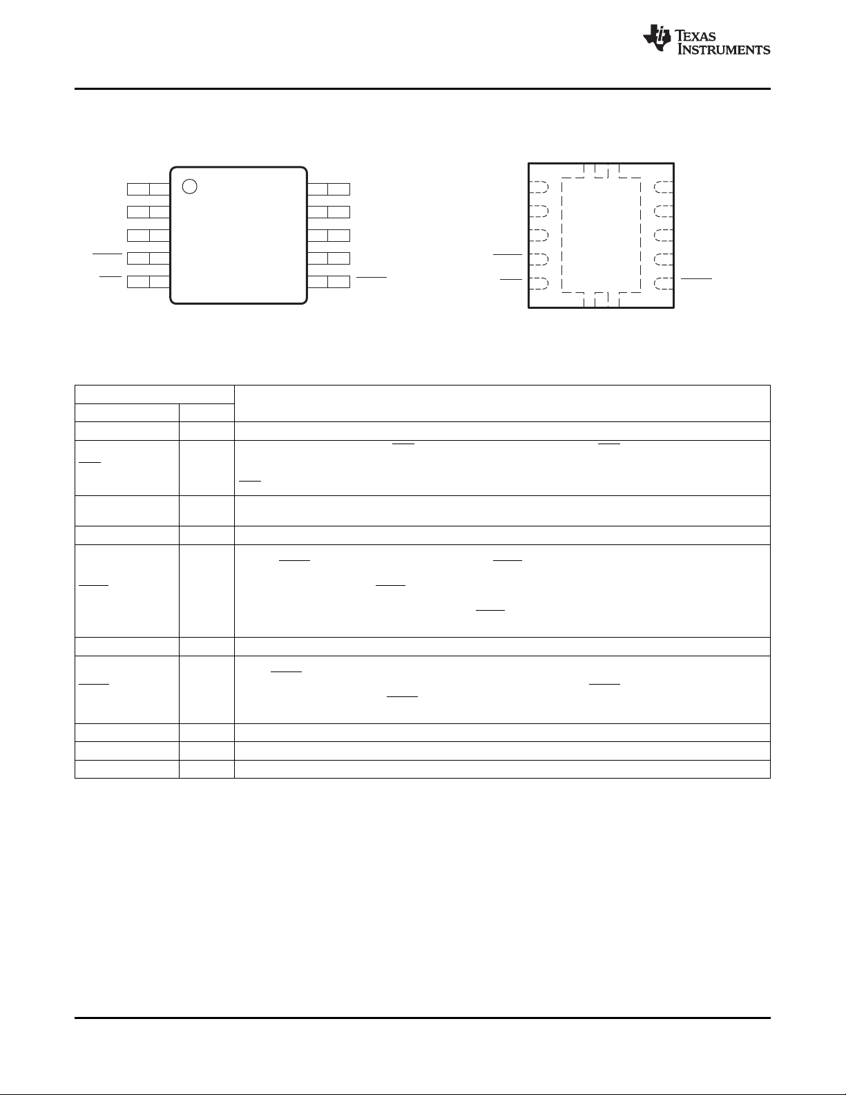
V A
OUT
V B
OUT
GND
LDAC
CLR
1
2
3
4
5
6
7
8
9
10
SYNC
SYNC
SCLK
SCLK
D
IN
D
IN
AV
DD
AV
DD
V /V
REFIN REFOUT
V /V
REFIN REFOUT
1
2
3
4
5
6
7
8
9
10
V A
OUT
V B
OUT
GND
LDAC
CLR
DGS
(Top View)
DSC
(Top View)
MSOP Package QFN Package
Thermal Pad
(1)
DAC8562, DAC8563
DAC8162, DAC8163
DAC7562, DAC7563
SLAS719C –AUGUST 2010– REVISED JUNE 2011
PIN CONFIGURATIONS
(1) It is recommended to connect the thermal pad to the ground plane for better thermal dissipation.
Table 2. PIN DESCRIPTIONS
PIN
NAME NO.
AV
DD
9 Power-supply input, 2.7 V to 5.5 V
Asynchronous clear input. The CLR input is falling-edge sensitive. When CLR is activated, zero scale
CLR 5
(DACxx62) or mid-scale (DACxx63) is loaded to all input and DAC registers. This sets the DAC output
voltages accordingly. The part exits clear code mode on the 24thfalling edge of the next write to the part. If
CLR is activated during a write sequence, the write is aborted.
D
IN
Serial data input. Data are clocked into the 24-bit input shift register on each falling edge of the serial clock
8
input. Schmitt-trigger logic input
GND 3 Ground reference point for all circuitry on the device
In synchronous mode, data are updated with the falling edge of the 24thSCLK cycle, which follows a falling
edge of SYNC. For such synchronous updates, the LDAC pin is not required, and it must be connected to
GND permanently or asserted and held low before sending commands to the device.
LDAC 4 In asynchronous mode, the LDAC pin is used as a negative edge-triggered timing signal for simultaneous
DAC updates. Multiple single-channel commands can be written in order to set different channel buffers to
desired values and then make a falling edge on LDAC pin to simultaneously update the DAC output
registers.
SCLK 7 Serial clock input. Data can be transferred at rates up to 50 MHz. Schmitt-trigger logic input
Level-triggered control input (active-low). This input is the frame synchronization signal for the input data.
When SYNC goes low, it enables the input shift register, and data are sampled on subsequent falling clock
SYNC 6 edges. The DAC output updates following the 24thclock falling edge. If SYNC is taken high before the 23
clock edge, the rising edge of SYNC acts as an interrupt, and the write sequence is ignored by the
DAC756x/DAC816x/DAC856x. Schmitt-trigger logic input
V
A 1 Analog output voltage from DAC-A
OUT
V
B 2 Analog output voltage from DAC-B
OUT
V
REFIN
/ V
REFOUT
10 Bidirectional voltage reference pin. If internal reference is used, 2.5-V output.
DESCRIPTION
www.ti.com
rd
6 Submit Documentation Feedback Copyright © 2010–2011, Texas Instruments Incorporated
Product Folder Link(s): DAC8562 DAC8563 DAC8162 DAC8163 DAC7562 DAC7563
Page 7

SCLK
SYNC
DIN
VOUT
DB23
DB0
LDAC
(1)
LDAC
(2)
CLR
t
2
t
7
t
6
t
9
t
10
t
8
t
4
t
5
t
3
t
1
t
12
t
13
t
14
t
11
www.ti.com
TIMING DIAGRAM
DAC8562, DAC8563
DAC8162, DAC8163
DAC7562, DAC7563
SLAS719C –AUGUST 2010– REVISED JUNE 2011
(1) Asynchronous LDAC update mode. For more information, see the LDAC Functionality section.
(2) Synchronous LDAC update mode; LDAC remains low. For more information, see the LDAC Functionality section.
Figure 1. Serial Write Operation
TIMING REQUIREMENTS
At AVDD= 2.7 V to 5.5 V and over –40°C to 125°C (unless otherwise noted).
t
1
(3)
t
2
t
3
t
4
t
5
t
6
t
7
t
8
t
9
t
10
t
11
t
12
t
13
t
14
(1) All input signals are specified with tR= tF= 3 ns (10% to 90% of AVDD) and timed from a voltage level of (VINL + VINH)/2.
(2) See the Serial Write Operation timing diagram (Figure 1).
(3) Maximum SCLK frequency is 50 MHz at AVDD= 2.7 V to 5.5 V.
SCLK falling edge to SYNC falling edge (for successful write operation) 10 ns
SCLK cycle time 20 ns
SYNC rising edge to 23rdSCLK falling edge (for successful SYNC interrupt) 13 ns
Minimum SYNC HIGH time 80 ns
SYNC to SCLK falling edge setup time 13 ns
SCLK LOW time 8 ns
SCLK HIGH time 8 ns
SCLK falling edge to SYNC rising edge 10 ns
Data setup time 6 ns
Data hold time 5 ns
SCLK falling edge to LDAC falling edge for asynchronous LDAC update mode 5 ns
LDAC pulse duration, LOW time 10 ns
CLR pulse duration, LOW time 80 ns
CLR falling edge to start of VOUT transition 100 ns
(1)(2)
PARAMETER UNIT
DAC756x/DAC816x/DAC856x
MIN TYP MAX
Copyright © 2010–2011, Texas Instruments Incorporated Submit Documentation Feedback 7
Product Folder Link(s): DAC8562 DAC8563 DAC8162 DAC8163 DAC7562 DAC7563
Page 8
DAC8562, DAC8563
DAC8162, DAC8163
DAC7562, DAC7563
SLAS719C –AUGUST 2010– REVISED JUNE 2011
TABLES OF GRAPHS
Table 3. Typical Characteristics: Internal Reference Performance
MEASUREMENT FIGURE NUMBER
Internal Reference Voltage vs Temperature Figure 2
Internal Reference Voltage Temperature Drift Histogram Figure 3
Internal Reference Voltage vs Load Current 5.5 V Figure 4
Internal Reference Voltage vs Time Figure 5
Internal Reference Noise Density vs Frequency Figure 6
Internal Reference Voltage vs Supply Voltage 2.7 V – 5.5 V Figure 7
Table 4. Typical Characteristics: DAC Static Performance
MEASUREMENT FIGURE NUMBER
FULL-SCALE, GAIN, OFFSET AND ZERO-CODE ERRORS
Full-Scale Error vs Temperature Figure 16
Gain Error vs Temperature Figure 17
Offset Error vs Temperature Figure 18
Zero-Code Error vs Temperature Figure 19
Full-Scale Error vs Temperature Figure 63
Gain Error vs Temperature Figure 64
Offset Error vs Temperature Figure 65
Zero-Code Error vs Temperature Figure 66
LOAD REGULATION
DAC Output Voltage vs Load Current
DIFFERENTIAL NONLINEARITY ERROR
T = –40°C Figure 9
Differential Linearity Error vs Digital Input Code T = 25°C Figure 11
T = 125°C Figure 13
Differential Linearity Error vs Temperature Figure 15
T = –40°C Figure 56
Differential Linearity Error vs Digital Input Code T = 25°C Figure 58
T = 125°C Figure 60
Differential Linearity Error vs Temperature Figure 62
INTEGRAL NONLINEARITY ERROR (RELATIVE ACCURACY)
T = –40°C Figure 8
Linearity Error vs Digital Input Code T = 25°C Figure 10
T = 125°C Figure 12
Linearity Error vs Temperature Figure 14
T = –40°C Figure 55
Linearity Error vs Digital Input Code T = 25°C Figure 57
T = 125°C Figure 59
Linearity Error vs Temperature Figure 61
POWER-SUPPLY
VOLTAGE
POWER-SUPPLY
VOLTAGE
5.5 V
2.7 V
5.5 V Figure 30
2.7 V Figure 74
5.5 V
2.7 V
5.5 V
2.7 V
www.ti.com
8 Submit Documentation Feedback Copyright © 2010–2011, Texas Instruments Incorporated
Product Folder Link(s): DAC8562 DAC8563 DAC8162 DAC8163 DAC7562 DAC7563
Page 9
DAC8562, DAC8563
DAC8162, DAC8163
DAC7562, DAC7563
www.ti.com
Table 4. Typical Characteristics: DAC Static Performance (continued)
MEASUREMENT FIGURE NUMBER
POWER-DOWN CURRENT
Power-Down Current vs Temperature 5.5 V Figure 28
Power-Down Current vs Power-Supply Voltage 2.7 V – 5.5 V Figure 29
Power-Down Current vs Temperature 2.7 V Figure 73
POWER-SUPPLY CURRENT
Power-Supply Current vs Temperature
Power-Supply Current vs Digital Input Code 5.5 V
Power-Supply Current Histogram
Power-Supply Current vs Power-Supply Voltage 2.7 V – 5.5 V
Power-Supply Current vs Temperature
Power-Supply Current vs Digital Input Code 3.6 V
Power-Supply Current Histogram
Power-Supply Current vs Temperature
Power-Supply Current vs Digital Input Code 2.7 V
Power-Supply Current Histogram
External V
Internal V
External V
Internal V
External V
Internal V
External V
Internal V
External V
Internal V
External V
Internal V
External V
Internal V
External V
Internal V
External V
Internal V
External V
Internal V
REF
REF
REF
REF
REF
REF
REF
REF
REF
REF
REF
REF
REF
REF
REF
REF
REF
REF
REF
REF
SLAS719C –AUGUST 2010– REVISED JUNE 2011
POWER-SUPPLY
VOLTAGE
Figure 20
Figure 21
Figure 22
Figure 23
Figure 24
Figure 25
Figure 26
Figure 27
Figure 49
Figure 50
Figure 51
Figure 52
Figure 53
Figure 54
Figure 67
Figure 68
Figure 69
Figure 70
Figure 71
Figure 72
Copyright © 2010–2011, Texas Instruments Incorporated Submit Documentation Feedback 9
Product Folder Link(s): DAC8562 DAC8563 DAC8162 DAC8163 DAC7562 DAC7563
Page 10
DAC8562, DAC8563
DAC8162, DAC8163
DAC7562, DAC7563
SLAS719C –AUGUST 2010– REVISED JUNE 2011
Table 5. Typical Characteristics: DAC Dynamic Performance
MEASUREMENT FIGURE NUMBER
CHANNEL-TO-CHANNEL CROSSTALK
Channel-to-Channel Crosstalk 5.5 V
CLOCK FEEDTHROUGH
Clock Feedthrough 500 kHz, Midscale
GLITCH ENERGY
Glitch Energy, 1-LSB Step
Glitch Energy, 4-LSB Step 5.5 V
Glitch Energy, 16-LSB Step
Glitch Energy, 1-LSB Step
Glitch Energy, 4-LSB Step 2.7 V
Glitch Energy, 16-LSB Step
NOISE
DAC Output Noise Density vs
Frequency
DAC Output Noise 0.1 Hz to 10 Hz External V
POWER-ON GLITCH
Power-on Glitch
SETTLING TIME
Full-Scale Settling Time
Half-Scale Settling Time
Full-Scale Settling Time
Half-Scale Settling Time
5-V Rising Edge Figure 43
5-V Falling Edge Figure 44
Rising Edge, Code 7FFFh to 8000h Figure 37
Falling Edge, Code 8000h to 7FFFh Figure 38
Rising Edge, Code 7FFCh to 8000h Figure 39
Falling Edge, Code 8000h to 7FFCh Figure 40
Rising Edge, Code 7FF0h to 8000h Figure 41
Falling Edge, Code 8000h to 7FF0h Figure 42
Rising Edge, Code 7FFFh to 8000h Figure 79
Falling Edge, Code 8000h to 7FFFh Figure 80
Rising Edge, Code 7FFCh to 8000h Figure 81
Falling Edge, Code 8000h to 7FFCh Figure 82
Rising Edge, Code 7FF0h to 8000h Figure 83
Falling Edge, Code 8000h to 7FF0h Figure 84
External V
Internal V
Reset to Zero Scale Figure 35
Reset to Midscale Figure 36
Reset to Zero Scale Figure 85
Reset to Midscale Figure 86
Rising Edge, Code 0h to FFFFh Figure 31
Falling Edge, Code FFFFh to 0h Figure 32
Rising Edge, Code 4000h to C000h Figure 33
Falling Edge, Code C000h to 4000h Figure 34
Rising Edge, Code 0h to FFFFh Figure 75
Falling Edge, Code FFFFh to 0h Figure 76
Rising Edge, Code 4000h to C000h Figure 77
Falling Edge, Code C000h to 4000h Figure 78
REF
REF
REF
POWER-SUPPLY
VOLTAGE
5.5 V Figure 48
2.7 V Figure 87
5.5 V Figure 46
5.5 V
2.7 V
5.5 V
2.7 V
www.ti.com
Figure 45
Figure 47
10 Submit Documentation Feedback Copyright © 2010–2011, Texas Instruments Incorporated
Product Folder Link(s): DAC8562 DAC8563 DAC8162 DAC8163 DAC7562 DAC7563
Page 11
2.495
2.496
2.497
2.498
2.499
2.500
2.501
2.502
2.503
2.504
2.505
−40 −25 −10 5 20 35 50 65 80 95 110 125
Temperature (°C)
V
REFOUT
(V)
60 units shown
(30 MSOP, 30 QFN−10)
Temperature Drift (ppm/ °C)
Population (%)
0.0
0.5
1.0
1.5
2.0
2.5
3.0
3.5
4.0
4.5
5.0
5.5
6.0
6.5
7.0
7.5
8.0
8.5
9.0
9.5
10.0
0
5
10
15
20
25
30
2.490
2.495
2.500
2.505
2.510
−20 −15 −10 −5 0 5 10 15 20
Load Current (mA)
V
REFOUT
(V)
0 250 500 750 1000 1250 1500
−400
−300
−200
−100
0
100
200
300
400
Elapsed Time (Hours)
Internal Reference Voltage Shift (ppm)
16 units shown (8 MSOP, 8 QFN−10)
Average shown in dashed line
0
50
100
150
200
250
300
350
400
10 100 1k 10k 100k 1M
Frequency (Hz)
Voltage Noise (nV/rt−Hz)
No Load
4.7 µF Load
2.495
2.496
2.497
2.498
2.499
2.500
2.501
2.502
2.503
2.504
2.505
2.7 3.1 3.5 3.9 4.3 4.7 5.1 5.5
AV
(V)
V
REFOUT
(V)
−40°C
+25°C
+125°C
www.ti.com
DAC8562, DAC8563
DAC8162, DAC8163
DAC7562, DAC7563
SLAS719C –AUGUST 2010– REVISED JUNE 2011
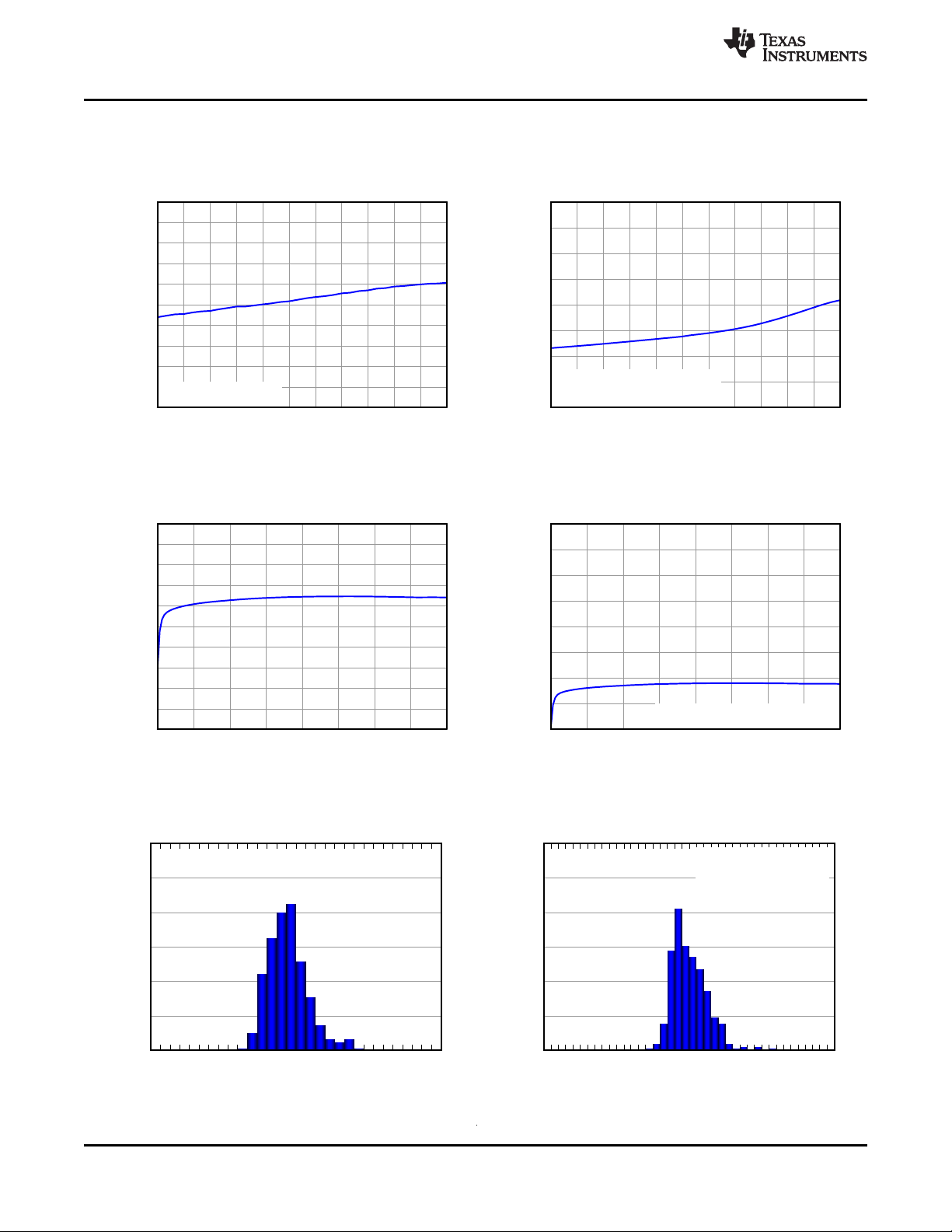
TYPICAL CHARACTERISTICS: Internal Reference
At TA= 25°C, AVDD= 5.5 V, gain = 2 and V
INTERNAL REFERENCE VOLTAGE INTERNAL REFERENCE VOLTAGE
vs TEMPERATURE TEMPERATURE DRIFT HISTOGRAM
Figure 2. Figure 3.
, unloaded unless otherwise noted.
REFOUT
INTERNAL REFERENCE VOLTAGE INTERNAL REFERENCE VOLTAGE
vs LOAD CURRENT vs TIME
Figure 4. Figure 5.
INTERNAL REFERENCE NOISE DENSITY INTERNAL REFERENCE VOLTAGE
vs FREQUENCY vs SUPPLY VOLTAGE
Copyright © 2010–2011, Texas Instruments Incorporated Submit Documentation Feedback 11
Product Folder Link(s): DAC8562 DAC8563 DAC8162 DAC8163 DAC7562 DAC7563
Figure 6. Figure 7.
Page 12
−12
−9
−6
−3
0
3
6
9
12
0 8192 16384 24576 32768 40960 49152 57344 65536
Digital Input Code
INL Error (LSB)
Typical channel shown
−40°C
−1.0
−0.8
−0.6
−0.4
−0.2
0.0
0.2
0.4
0.6
0.8
1.0
0 8192 16384 24576 32768 40960 49152 57344 65536
Digital Input Code
DNL Error (LSB)
Typical channel shown
−40°C
−12
−9
−6
−3
0
3
6
9
12
0 8192 16384 24576 32768 40960 49152 57344 65536
Digital Input Code
INL Error (LSB)
Typical channel shown
25°C
−1.0
−0.8
−0.6
−0.4
−0.2
0.0
0.2
0.4
0.6
0.8
1.0
0 8192 16384 24576 32768 40960 49152 57344 65536
Digital Input Code
DNL Error (LSB)
Typical channel shown
25°C
−12
−9
−6
−3
0
3
6
9
12
0 8192 16384 24576 32768 40960 49152 57344 65536
Digital Input Code
INL Error (LSB)
Typical channel shown
125°C
−1.0
−0.8
−0.6
−0.4
−0.2
0.0
0.2
0.4
0.6
0.8
1.0
0 8192 16384 24576 32768 40960 49152 57344 65536
Digital Input Code
DNL Error (LSB)
Typical channel shown
125°C
DAC8562, DAC8563
DAC8162, DAC8163
DAC7562, DAC7563
SLAS719C –AUGUST 2010– REVISED JUNE 2011
TYPICAL CHARACTERISTICS: DAC at AVDD= 5.5 V
At TA= 25°C, 5-V external reference used, gain = 1 and DAC output not loaded, unless otherwise noted.
LINEARITY ERROR DIFFERENTIAL LINEARITY ERROR
vs DIGITAL INPUT CODE (–40°C) vs DIGITAL INPUT CODE (–40°C)
Figure 8. Figure 9.
www.ti.com
LINEARITY ERROR DIFFERENTIAL LINEARITY ERROR
vs DIGITAL INPUT CODE (25°C) vs DIGITAL INPUT CODE (25°C)
Figure 10. Figure 11.
LINEARITY ERROR DIFFERENTIAL LINEARITY ERROR
vs DIGITAL INPUT CODE (125°C) vs DIGITAL INPUT CODE (125°C)
12 Submit Documentation Feedback Copyright © 2010–2011, Texas Instruments Incorporated
Figure 12. Figure 13.
Product Folder Link(s): DAC8562 DAC8563 DAC8162 DAC8163 DAC7562 DAC7563
Page 13
−12
−9
−6
−3
0
3
6
9
12
−40 −25 −10 5 20 35 50 65 80 95 110 125
Temperature (°C)
INL Error (LSB)
INL Max
INL Min
Typical channel shown
−1.0
−0.8
−0.6
−0.4
−0.2
0.0
0.2
0.4
0.6
0.8
1.0
−40 −25 −10 5 20 35 50 65 80 95 110 125
Temperature (°C)
DNL Error (LSB)
DNL Max
DNL Min
Typical channel shown
−0.20
−0.15
−0.10
−0.05
0.00
0.05
0.10
0.15
0.20
−40 −25 −10 5 20 35 50 65 80 95 110 125
Temperature (°C)
Full−Scale Error (%FSR)
Ch A
Ch B
−0.15
−0.10
−0.05
0.00
0.05
0.10
0.15
−40 −25 −10 5 20 35 50 65 80 95 110 125
Temperature (°C)
Gain Error (%FSR)
Ch A
Ch B
−4
−3
−2
−1
0
1
2
3
4
−40 −25 −10 5 20 35 50 65 80 95 110 125
Temperature (°C)
Offset Error (mV)
Ch A
Ch B
0.0
0.5
1.0
1.5
2.0
2.5
3.0
3.5
4.0
−40 −25 −10 5 20 35 50 65 80 95 110 125
Temperature (°C)
Zero−Code Error (mV)
Ch A
Ch B
DAC8562, DAC8563
DAC8162, DAC8163
DAC7562, DAC7563
www.ti.com
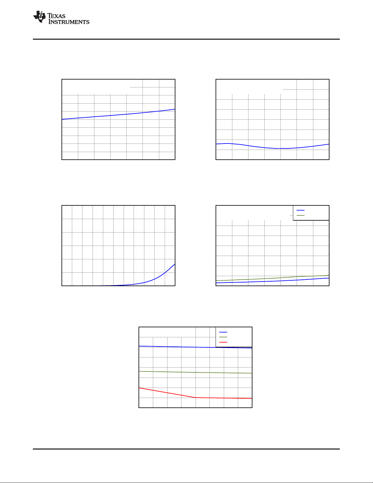
TYPICAL CHARACTERISTICS: DAC at AVDD= 5.5 V (continued)
At TA= 25°C, 5-V external reference used, gain = 1 and DAC output not loaded, unless otherwise noted.
LINEARITY ERROR DIFFERENTIAL LINEARITY ERROR
vs TEMPERATURE vs TEMPERATURE
Figure 14. Figure 15.
SLAS719C –AUGUST 2010– REVISED JUNE 2011
FULL-SCALE ERROR GAIN ERROR
vs TEMPERATURE vs TEMPERATURE
Figure 16. Figure 17.
OFFSET ERROR ZERO-CODE ERROR
vs TEMPERATURE vs TEMPERATURE
Copyright © 2010–2011, Texas Instruments Incorporated Submit Documentation Feedback 13
Figure 18. Figure 19.
Product Folder Link(s): DAC8562 DAC8563 DAC8162 DAC8163 DAC7562 DAC7563
Page 14
0.00
0.05
0.10
0.15
0.20
0.25
0.30
0.35
0.40
0.45
0.50
−40 −25 −10 5 20 35 50 65 80 95 110 125
Temperature (°C)
Power−Supply Current (mA)
DACs at midscale code
0.5
0.6
0.7
0.8
0.9
1.0
1.1
1.2
1.3
−40 −25 −10 5 20 35 50 65 80 95 110 125
Temperature (°C)
Power−Supply Current (mA)
Internal reference enabled
DACs at midscale code, Gain = 2
0.00
0.05
0.10
0.15
0.20
0.25
0.30
0.35
0.40
0.45
0.50
0 8192 16384 24576 32768 40960 49152 57344 65536
Digital Input Code
Power−Supply Current (mA)
0.5
0.6
0.7
0.8
0.9
1.0
1.1
1.2
1.3
0 8192 16384 24576 32768 40960 49152 57344 65536
Digital Input Code
Power−Supply Current (mA)
Internal reference enabled, Gain = 2
Power Supply Current (mA)
Population (%)
0.15
0.17
0.19
0.21
0.23
0.25
0.27
0.29
0.31
0.33
0.35
0.37
0.39
0.41
0.43
0.45
0
5
10
15
20
25
30
Power Supply Current (mA)
Population (%)
0.30
0.35
0.40
0.45
0.50
0.55
0.60
0.65
0.70
0.75
0.80
0.85
0.90
0.95
1.00
1.05
1.10
1.15
1.20
1.25
1.30
0
5
10
15
20
25
30
Internal reference enabled
Gain = 2
DAC8562, DAC8563
DAC8162, DAC8163
DAC7562, DAC7563
SLAS719C –AUGUST 2010– REVISED JUNE 2011
TYPICAL CHARACTERISTICS: DAC at AVDD= 5.5 V (continued)
At TA= 25°C, 5-V external reference used, gain = 1 and DAC output not loaded, unless otherwise noted.
POWER-SUPPLY CURRENT POWER-SUPPLY CURRENT
vs TEMPERATURE vs TEMPERATURE
Figure 20. Figure 21.
www.ti.com
POWER-SUPPLY CURRENT POWER-SUPPLY CURRENT
vs DIGITAL INPUT CODE vs DIGITAL INPUT CODE
Figure 22. Figure 23.
POWER-SUPPLY CURRENT POWER-SUPPLY CURRENT
HISTOGRAM HISTOGRAM
14 Submit Documentation Feedback Copyright © 2010–2011, Texas Instruments Incorporated
Figure 24. Figure 25.
Product Folder Link(s): DAC8562 DAC8563 DAC8162 DAC8163 DAC7562 DAC7563
Page 15
0.00
0.05
0.10
0.15
0.20
0.25
0.30
0.35
0.40
0.45
0.50
2.7 3.1 3.5 3.9 4.3 4.7 5.1 5.5
AV
(V)
Power−Supply Current (mA)
V
REFIN
= 2.5 V
DACs at midscale code, Gain = 1
0.5
0.6
0.7
0.8
0.9
1.0
1.1
1.2
1.3
2.7 3.1 3.5 3.9 4.3 4.7 5.1 5.5
AV
(V)
Power−Supply Current (mA)
Internal reference enabled
DACs at midscale code, Gain = 1
0.0
0.5
1.0
1.5
2.0
2.5
3.0
−40 −25 −10 5 20 35 50 65 80 95 110 125
Temperature (°C)
Power−Down Current (µA)
0.000
0.005
0.010
0.015
0.020
0.025
0.030
0.035
0.040
2.7 3.1 3.5 3.9 4.3 4.7 5.1 5.5
AV
(V)
Power−Down Current (µA)
IDD (µA)
I
REFIN
(µA)
Both channels and internal reference
in power−down mode; V
REFIN
= A
VDD
−1.0
0.0
1.0
2.0
3.0
4.0
5.0
6.0
7.0
−20 −15 −10 −5 0 5 10 15 20
I
(mA)
Output Voltage (V)
Full scale
Mid scale
Zero scale
Typical channel shown
DAC8562, DAC8563
DAC8162, DAC8163
DAC7562, DAC7563
www.ti.com
TYPICAL CHARACTERISTICS: DAC at AVDD= 5.5 V (continued)
At TA= 25°C, 5-V external reference used, gain = 1 and DAC output not loaded, unless otherwise noted.
POWER-SUPPLY CURRENT POWER-SUPPLY CURRENT
vs POWER-SUPPLY VOLTAGE vs POWER-SUPPLY VOLTAGE
Figure 26. Figure 27.
SLAS719C –AUGUST 2010– REVISED JUNE 2011
POWER-DOWN CURRENT POWER-DOWN CURRENT
vs TEMPERATURE vs POWER-SUPPLY VOLTAGE
Figure 28. Figure 29.
DAC OUTPUT VOLTAGE
vs LOAD CURRENT
Copyright © 2010–2011, Texas Instruments Incorporated Submit Documentation Feedback 15
Product Folder Link(s): DAC8562 DAC8563 DAC8162 DAC8163 DAC7562 DAC7563
Figure 30.
Page 16
Time (5 s/div)μ
Trigger (5 V/div)LDAC
Large Signal V (2 V/div)
OUT
Small Signal Settling
(1.22 mV/div = 0.024% FSR)
From Code:
To Code:0hFFFFh
Time (5 s/div)μ
Trigger (5 V/div)LDAC
Large Signal V (2 V/div)
OUT
Small Signal Settling (1.22 mV/div = 0.024% FSR)
From Code: FFFF
To Code: 0hh
Time (5 s/div)μ
Trigger (5 V/div)LDAC
Large Signal V (2 V/div)
OUT
Small Signal Settling (1.22 mV/div = 0.024% FSR)
From Code:
To Code:
4000h
C000h
Time (5 s/div)μ
Trigger (5 V/div)LDAC
Large Signal V (2 V/div)
OUT
Small Signal Settling (1.22 mV/div = 0.024% FSR)
From Code: C000h
To Code: 4000h
Time (1 ms/div)
AV (2 V/div)
DD
V A (50 mV/div)
OUT
V shorted to
REFIN
AV
DD
V B (50 mV/div)
OUT
Time (1 ms/div)
AV (2 V/div)
DD
V A (1 V/div)
OUT
V shorted to
REFIN
AV
DD
V B (1 V/div)
OUT
DAC8562, DAC8563
DAC8162, DAC8163
DAC7562, DAC7563
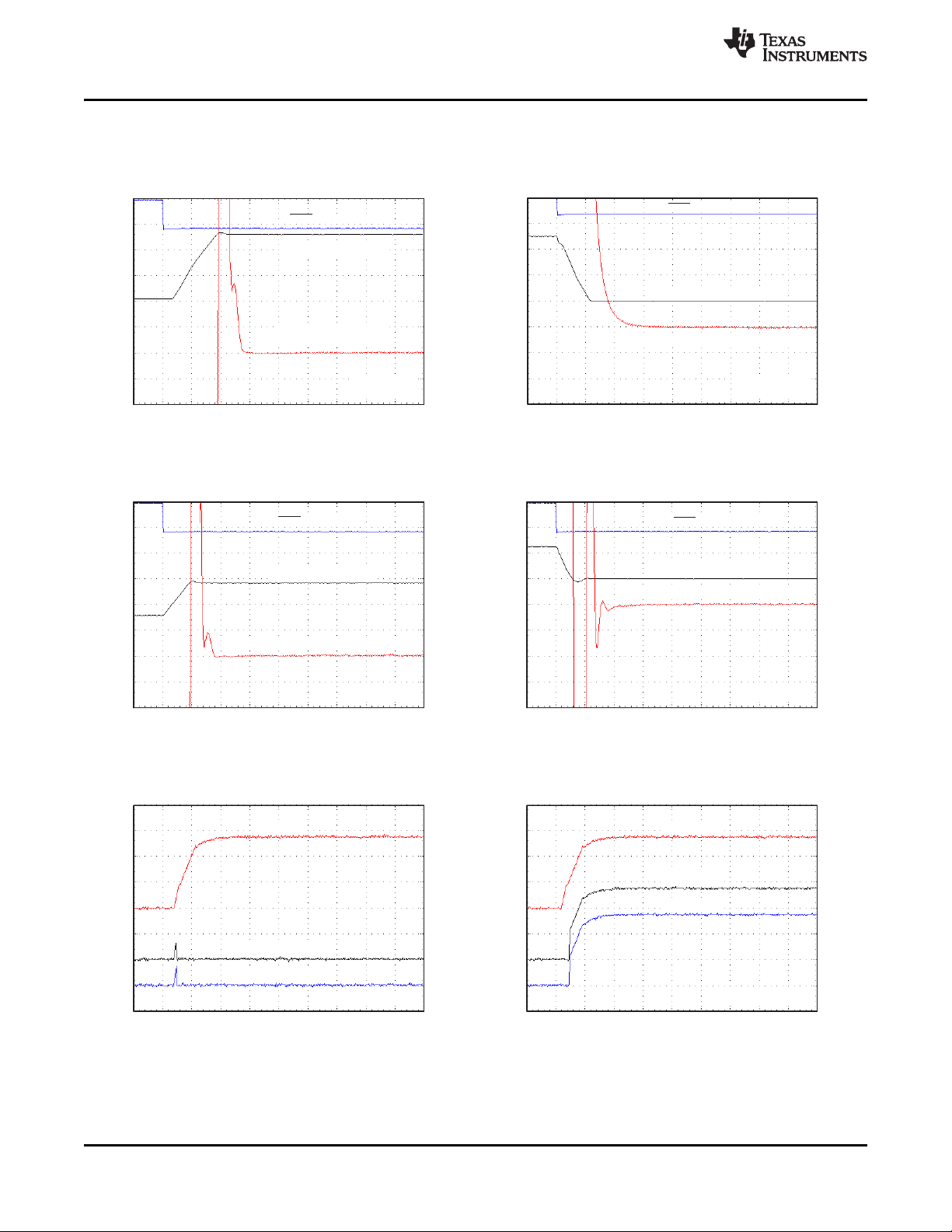
SLAS719C –AUGUST 2010– REVISED JUNE 2011
TYPICAL CHARACTERISTICS: DAC at AVDD= 5.5 V (continued)
At TA= 25°C, 5-V external reference used, gain = 1 and DAC output not loaded, unless otherwise noted.
FULL-SCALE SETTLING TIME: FULL-SCALE SETTLING TIME:
RISING EDGE FALLING EDGE
Figure 31. Figure 32.
HALF-SCALE SETTLING TIME: HALF-SCALE SETTLING TIME:
RISING EDGE FALLING EDGE
www.ti.com
Figure 33. Figure 34.
POWER-ON GLITCH POWER-ON GLITCH
RESET TO ZERO SCALE RESET TO MIDSCALE
16 Submit Documentation Feedback Copyright © 2010–2011, Texas Instruments Incorporated
Figure 35. Figure 36.
Product Folder Link(s): DAC8562 DAC8563 DAC8162 DAC8163 DAC7562 DAC7563
Page 17

Time (5 s/div)μ
V (100 V/div)
OUT
μ
From Code: 7FFFh
To Code: 8000h
Trigger (5 V/div)LDAC
FeedthroughLDAC
Glitch Impulse 0.1 nV-s»
Time (5 s/div)μ
V (100 V/div)
OUT
μ
From Code:
To Code:
8000h
7FFFh
Trigger (5 V/div)LDAC
FeedthroughLDAC
Glitch Impulse 0.12 nV-s»
Time (5 s/div)μ
V (100 V/div)
OUT
μ
From Code: 7FFCh
To Code: 8000h
Trigger (5 V/div)LDAC
FeedthroughLDAC
Glitch Impulse 0.1 nV-s»
Time (5 s/div)μ
V (100 V/div)
OUT
μ
From Code:
To Code:
8000h
7FFCh
Trigger (5 V/div)LDAC
FeedthroughLDAC
Glitch Impulse 0.14 nV-s»
Time (5 s/div)μ
V (500 V/div)
OUT
μ
From Code: 7FF0h
To Code: 8000h
Trigger (5 V/div)LDAC
FeedthroughLDAC
Glitch Impulse 0.1 nV-s»
Time (5 s/div)μ
V (500 V/div)
OUT
μ
From Code:
To Code:
8000h
7FF0h
Trigger (5 V/div)LDAC
FeedthroughLDAC
Glitch Impulse 0.1 nV-s»
DAC8562, DAC8563
DAC8162, DAC8163
DAC7562, DAC7563
www.ti.com
TYPICAL CHARACTERISTICS: DAC at AVDD= 5.5 V (continued)
At TA= 25°C, 5-V external reference used, gain = 1 and DAC output not loaded, unless otherwise noted.
GLITCH ENERGY GLITCH ENERGY
RISING EDGE, 1-LSB STEP FALLING EDGE, 1-LSB STEP
Figure 37. Figure 38.
GLITCH ENERGY GLITCH ENERGY
RISING EDGE, 4-LSB STEP FALLING EDGE, 4-LSB STEP
SLAS719C –AUGUST 2010– REVISED JUNE 2011
Figure 39. Figure 40.
GLITCH ENERGY GLITCH ENERGY
RISING EDGE, 16-LSB STEP FALLING EDGE, 16-LSB STEP
Figure 41. Figure 42.
Copyright © 2010–2011, Texas Instruments Incorporated Submit Documentation Feedback 17
Product Folder Link(s): DAC8562 DAC8563 DAC8162 DAC8163 DAC7562 DAC7563
Page 18

Time (5 s/div)μ
V B (1 V/div)
OUT
V A (500 V/div)
OUT
μ
V A at Midscale Code
Internal Reference Enabled
Gain = 2
OUT
Trigger (5 V/div)LDAC
Glitch Area (Between Cursors) = 1.6 nV-s
7.3 sμ
Time (5 s/div)μ
V B (1 V/div)
OUT
V A (500 V/div)
OUT
μ
V A at Midscale Code
Internal Reference Enabled
Gain = 2
OUT
Trigger (5 V/div)LDAC
Glitch Area (Between Cursors) = 2 nV-s
6.4 sμ
0
200
400
600
800
1000
1200
1400
10 100 1k 10k 100k
Frequency (Hz)
Voltage Noise (nV/rt−Hz)
Full Scale
Mid Scale
Zero Scale
Internal reference disabled
V
REFIN
= 5 V, Gain = 1
0
200
400
600
800
1000
1200
1400
10 100 1k 10k 100k
Frequency (Hz)
Voltage Noise (nV/rt−Hz)
Full Scale
Mid Scale
Zero Scale
Internal reference enabled
Gain = 2
V (1 V/div)
NOISE
μ
DAC = Midscale
2.5» μV
PP
Time (500 ns/div)
SCLK (5 V/div)
V (500 V/div)
OUT
μ
Clock Feedthrough Impulse 0.06 nV-s»
DAC8562, DAC8563
DAC8162, DAC8163
DAC7562, DAC7563
SLAS719C –AUGUST 2010– REVISED JUNE 2011
TYPICAL CHARACTERISTICS: DAC at AVDD= 5.5 V (continued)
At TA= 25°C, 5-V external reference used, gain = 1 and DAC output not loaded, unless otherwise noted.
CHANNEL-TO-CHANNEL CROSSTALK CHANNEL-TO-CHANNEL CROSSTALK
5-V RISING EDGE 5-V FALLING EDGE
Figure 43. Figure 44.
DAC OUTPUT NOISE DENSITY DAC OUTPUT NOISE DENSITY
vs FREQUENCY vs FREQUENCY
www.ti.com
18 Submit Documentation Feedback Copyright © 2010–2011, Texas Instruments Incorporated
DAC OUTPUT NOISE CLOCK FEEDTHROUGH
Product Folder Link(s): DAC8562 DAC8563 DAC8162 DAC8163 DAC7562 DAC7563
Figure 45. Figure 46.
0.1 Hz TO 10 Hz 500 kHz, MIDSCALE
Figure 47. Figure 48.
Page 19

0.00
0.05
0.10
0.15
0.20
0.25
0.30
0.35
0.40
0.45
0.50
−40 −25 −10 5 20 35 50 65 80 95 110 125
Temperature (°C)
Power−Supply Current (mA)
DACs at midscale code
0.5
0.6
0.7
0.8
0.9
1.0
1.1
1.2
1.3
−40 −25 −10 5 20 35 50 65 80 95 110 125
Temperature (°C)
Power−Supply Current (mA)
Internal reference enabled
DACs at midscale code, Gain = 1
0.00
0.05
0.10
0.15
0.20
0.25
0.30
0.35
0.40
0.45
0.50
0 8192 16384 24576 32768 40960 49152 57344 65536
Digital Input Code
Power−Supply Current (mA)
0.4
0.5
0.6
0.7
0.8
0.9
1.0
1.1
1.2
1.3
0 8192 16384 24576 32768 40960 49152 57344 65536
Digital Input Code
Power−Supply Current (mA)
Internal reference enabled, Gain = 1
Power Supply Current (mA)
Population (%)
0.10
0.12
0.14
0.16
0.18
0.20
0.22
0.24
0.26
0.28
0.30
0.32
0.34
0.36
0.38
0.40
0
5
10
15
20
25
30
Power Supply Current (mA)
Population (%)
0.30
0.35
0.40
0.45
0.50
0.55
0.60
0.65
0.70
0.75
0.80
0.85
0.90
0.95
1.00
1.05
1.10
1.15
1.20
1.25
1.30
0
5
10
15
20
25
30
Internal reference enabled
Gain = 1
www.ti.com
DAC8562, DAC8563
DAC8162, DAC8163
DAC7562, DAC7563
SLAS719C –AUGUST 2010– REVISED JUNE 2011
TYPICAL CHARACTERISTICS: DAC at AVDD= 3.6 V
At TA= 25°C, 3.3-V external reference used, gain = 1 and DAC output not loaded, unless otherwise noted.
POWER-SUPPLY CURRENT POWER-SUPPLY CURRENT
vs TEMPERATURE vs TEMPERATURE
Figure 49. Figure 50.
POWER-SUPPLY CURRENT POWER-SUPPLY CURRENT
vs DIGITAL INPUT CODE vs DIGITAL INPUT CODE
Figure 51. Figure 52.
POWER-SUPPLY CURRENT POWER-SUPPLY CURRENT
HISTOGRAM HISTOGRAM
Copyright © 2010–2011, Texas Instruments Incorporated Submit Documentation Feedback 19
Figure 53. Figure 54.
Product Folder Link(s): DAC8562 DAC8563 DAC8162 DAC8163 DAC7562 DAC7563
Page 20

−12
−9
−6
−3
0
3
6
9
12
0 8192 16384 24576 32768 40960 49152 57344 65536
Digital Input Code
INL Error (LSB)
Typical channel shown
−40°C
−1.0
−0.8
−0.6
−0.4
−0.2
0.0
0.2
0.4
0.6
0.8
1.0
0 8192 16384 24576 32768 40960 49152 57344 65536
Digital Input Code
DNL Error (LSB)
Typical channel shown
−40°C
−12
−9
−6
−3
0
3
6
9
12
0 8192 16384 24576 32768 40960 49152 57344 65536
Digital Input Code
INL Error (LSB)
Typical channel shown
25°C
−1.0
−0.8
−0.6
−0.4
−0.2
0.0
0.2
0.4
0.6
0.8
1.0
0 8192 16384 24576 32768 40960 49152 57344 65536
Digital Input Code
DNL Error (LSB)
Typical channel shown
25°C
−12
−9
−6
−3
0
3
6
9
12
0 8192 16384 24576 32768 40960 49152 57344 65536
Digital Input Code
INL Error (LSB)
Typical channel shown
125°C
−1.0
−0.8
−0.6
−0.4
−0.2
0.0
0.2
0.4
0.6
0.8
1.0
0 8192 16384 24576 32768 40960 49152 57344 65536
Digital Input Code
DNL Error (LSB)
Typical channel shown
125°C
DAC8562, DAC8563
DAC8162, DAC8163
DAC7562, DAC7563
SLAS719C –AUGUST 2010– REVISED JUNE 2011
TYPICAL CHARACTERISTICS: DAC at AVDD= 2.7 V
At TA= 25°C, 2.5-V external reference used, gain = 1 and DAC output not loaded, unless otherwise noted.
LINEARITY ERROR DIFFERENTIAL LINEARITY ERROR
vs DIGITAL INPUT CODE (–40°C) vs DIGITAL INPUT CODE (–40°C)
Figure 55. Figure 56.
www.ti.com
LINEARITY ERROR DIFFERENTIAL LINEARITY ERROR
vs DIGITAL INPUT CODE (25°C) vs DIGITAL INPUT CODE (25°C)
Figure 57. Figure 58.
LINEARITY ERROR DIFFERENTIAL LINEARITY ERROR
vs DIGITAL INPUT CODE (125°C) vs DIGITAL INPUT CODE (125°C)
20 Submit Documentation Feedback Copyright © 2010–2011, Texas Instruments Incorporated
Figure 59. Figure 60.
Product Folder Link(s): DAC8562 DAC8563 DAC8162 DAC8163 DAC7562 DAC7563
Page 21

−12
−9
−6
−3
0
3
6
9
12
−40 −25 −10 5 20 35 50 65 80 95 110 125
Temperature (°C)
INL Error (LSB)
INL Max
INL Min
Typical channel shown
−1.0
−0.8
−0.6
−0.4
−0.2
0.0
0.2
0.4
0.6
0.8
1.0
−40 −25 −10 5 20 35 50 65 80 95 110 125
Temperature (°C)
DNL Error (LSB)
DNL Max
DNL Min
Typical channel shown
−0.20
−0.15
−0.10
−0.05
0.00
0.05
0.10
0.15
0.20
−40 −25 −10 5 20 35 50 65 80 95 110 125
Temperature (°C)
Full−Scale Error (%FSR)
Ch A
Ch B
−0.15
−0.10
−0.05
0.00
0.05
0.10
0.15
−40 −25 −10 5 20 35 50 65 80 95 110 125
Temperature (°C)
Gain Error (%FSR)
Ch A
Ch B
−4
−3
−2
−1
0
1
2
3
4
−40 −25 −10 5 20 35 50 65 80 95 110 125
Temperature (°C)
Offset Error (mV)
Ch A
Ch B
0.0
0.5
1.0
1.5
2.0
2.5
3.0
3.5
4.0
−40 −25 −10 5 20 35 50 65 80 95 110 125
Temperature (°C)
Zero−Code Error (mV)
Ch A
Ch B
DAC8562, DAC8563
DAC8162, DAC8163
DAC7562, DAC7563
www.ti.com
TYPICAL CHARACTERISTICS: DAC at AVDD= 2.7 V (continued)
At TA= 25°C, 2.5-V external reference used, gain = 1 and DAC output not loaded, unless otherwise noted.
LINEARITY ERROR DIFFERENTIAL LINEARITY ERROR
vs TEMPERATURE vs TEMPERATURE
Figure 61. Figure 62.
SLAS719C –AUGUST 2010– REVISED JUNE 2011
FULL-SCALE ERROR GAIN ERROR
vs TEMPERATURE vs TEMPERATURE
Figure 63. Figure 64.
OFFSET ERROR ZERO-CODE ERROR
vs TEMPERATURE vs TEMPERATURE
Copyright © 2010–2011, Texas Instruments Incorporated Submit Documentation Feedback 21
Figure 65. Figure 66.
Product Folder Link(s): DAC8562 DAC8563 DAC8162 DAC8163 DAC7562 DAC7563
Page 22

0.00
0.05
0.10
0.15
0.20
0.25
0.30
0.35
0.40
−40 −25 −10 5 20 35 50 65 80 95 110 125
Temperature (°C)
Power−Supply Current (mA)
DACs at midscale code
0.5
0.6
0.7
0.8
0.9
1.0
1.1
1.2
1.3
−40 −25 −10 5 20 35 50 65 80 95 110 125
Temperature (°C)
Power−Supply Current (mA)
Internal reference enabled
DACs at midscale code, Gain = 1
0.00
0.05
0.10
0.15
0.20
0.25
0.30
0.35
0.40
0 8192 16384 24576 32768 40960 49152 57344 65536
Digital Input Code
Power−Supply Current (mA)
0.4
0.5
0.6
0.7
0.8
0.9
1.0
1.1
1.2
1.3
0 8192 16384 24576 32768 40960 49152 57344 65536
Digital Input Code
Power−Supply Current (mA)
Internal reference enabled, Gain = 1
Power Supply Current (mA)
Population (%)
0.10
0.12
0.14
0.16
0.18
0.20
0.22
0.24
0.26
0.28
0.30
0.32
0.34
0.36
0.38
0.40
0
5
10
15
20
25
30
Power Supply Current (mA)
Population (%)
0.30
0.35
0.40
0.45
0.50
0.55
0.60
0.65
0.70
0.75
0.80
0.85
0.90
0.95
1.00
1.05
1.10
1.15
1.20
1.25
1.30
0
5
10
15
20
25
30
Internal reference enabled
Gain = 1
DAC8562, DAC8563
DAC8162, DAC8163
DAC7562, DAC7563
SLAS719C –AUGUST 2010– REVISED JUNE 2011
TYPICAL CHARACTERISTICS: DAC at AVDD= 2.7 V (continued)
At TA= 25°C, 2.5-V external reference used, gain = 1 and DAC output not loaded, unless otherwise noted.
POWER-SUPPLY CURRENT POWER-SUPPLY CURRENT
vs TEMPERATURE vs TEMPERATURE
Figure 67. Figure 68.
www.ti.com
POWER-SUPPLY CURRENT POWER-SUPPLY CURRENT
vs DIGITAL INPUT CODE vs DIGITAL INPUT CODE
Figure 69. Figure 70.
POWER-SUPPLY CURRENT POWER-SUPPLY CURRENT
HISTOGRAM HISTOGRAM
22 Submit Documentation Feedback Copyright © 2010–2011, Texas Instruments Incorporated
Figure 71. Figure 72.
Product Folder Link(s): DAC8562 DAC8563 DAC8162 DAC8163 DAC7562 DAC7563
Page 23

0.0
0.5
1.0
1.5
2.0
2.5
3.0
−40 −25 −10 5 20 35 50 65 80 95 110 125
Temperature (°C)
Power−Down Current (µA)
−1
0
1
2
3
4
−20 −15 −10 −5 0 5 10 15 20
I
(mA)
Output Voltage (V)
Full scale
Mid scale
Zero scale
Typical channel shown
Time (5 s/div)μ
Trigger (5 V/div)LDAC
Large Signal V (1 V/div)
OUT
Small Signal Settling (0.61 mV/div = 0.024% FSR)
From Code:
To Code:0hFFFFh
Time (5 s/div)μ
Trigger (5 V/div)LDAC
Large Signal V (1 V/div)
OUT
Small Signal Settling (0.61 mV/div = 0.024% FSR)
From Code: FFFF
To Code: 0hh
Time (5 s/div)μ
Trigger (5 V/div)LDAC
Large Signal V (1 V/div)
OUT
Small Signal Settling (0.61 mV/div = 0.024% FSR)
From Code:
To Code:
4000h
C000h
Time (5 s/div)μ
Trigger (5 V/div)LDAC
Large Signal V (1 V/div)
OUT
Small Signal Settling (0.61 mV/div = 0.024% FSR)
From Code: C000h
To Code: 4000h
DAC8562, DAC8563
DAC8162, DAC8163
DAC7562, DAC7563
www.ti.com
TYPICAL CHARACTERISTICS: DAC at AVDD= 2.7 V (continued)
At TA= 25°C, 2.5-V external reference used, gain = 1 and DAC output not loaded, unless otherwise noted.
POWER-DOWN CURRENT DAC OUTPUT VOLTAGE
vs TEMPERATURE vs LOAD CURRENT
Figure 73. Figure 74.
SLAS719C –AUGUST 2010– REVISED JUNE 2011
FULL-SCALE SETTLING TIME: FULL-SCALE SETTLING TIME:
RISING EDGE FALLING EDGE
Figure 75. Figure 76.
HALF-SCALE SETTLING TIME: HALF-SCALE SETTLING TIME:
RISING EDGE FALLING EDGE
Copyright © 2010–2011, Texas Instruments Incorporated Submit Documentation Feedback 23
Figure 77. Figure 78.
Product Folder Link(s): DAC8562 DAC8563 DAC8162 DAC8163 DAC7562 DAC7563
Page 24

Time (5 s/div)μ
V (100 V/div)
OUT
μ
From Code: 7FFFh
To Code: 8000h
Trigger (5 V/div)LDAC
FeedthroughLDAC
Glitch Impulse 0.1 nV-s»
Time (5 s/div)μ
V (100 V/div)
OUT
μ
From Code:
To Code:
8000h
7FFFh
Trigger (5 V/div)LDAC
FeedthroughLDAC
Glitch Impulse 0.1 nV-s»
Time (5 s/div)μ
V (100 V/div)
OUT
μ
From Code: 7FFCh
To Code: 8000h
Trigger (5 V/div)LDAC
FeedthroughLDAC
Glitch Impulse 0.1 nV-s»
Time (5 s/div)μ
V (100 V/div)
OUT
μ
From Code:
To Code:
8000h
7FFCh
Trigger (5 V/div)LDAC
FeedthroughLDAC
Glitch Impulse 0.1 nV-s»
Time (5 s/div)μ
V (200 V/div)
OUT
μ
From Code: 7FF0h
To Code: 8000h
Trigger (5 V/div)LDAC
FeedthroughLDAC
Glitch Impulse 0.1 nV-s»
Time (5 s/div)μ
V (200 V/div)
OUT
μ
From Code:
To Code:
8000h
7FF0h
Trigger (5 V/div)LDAC
Glitch Impulse 0.1 nV-s»
FeedthroughLDAC
DAC8562, DAC8563
DAC8162, DAC8163
DAC7562, DAC7563
SLAS719C –AUGUST 2010– REVISED JUNE 2011
TYPICAL CHARACTERISTICS: DAC at AVDD= 2.7 V (continued)
At TA= 25°C, 2.5-V external reference used, gain = 1 and DAC output not loaded, unless otherwise noted.
GLITCH ENERGY GLITCH ENERGY
RISING EDGE, 1-LSB STEP FALLING EDGE, 1-LSB STEP
Figure 79. Figure 80.
GLITCH ENERGY GLITCH ENERGY
RISING EDGE, 4-LSB STEP FALLING EDGE, 4-LSB STEP
www.ti.com
Figure 81. Figure 82.
GLITCH ENERGY GLITCH ENERGY
RISING EDGE, 16-LSB STEP FALLING EDGE, 16-LSB STEP
Figure 83. Figure 84.
24 Submit Documentation Feedback Copyright © 2010–2011, Texas Instruments Incorporated
Product Folder Link(s): DAC8562 DAC8563 DAC8162 DAC8163 DAC7562 DAC7563
Page 25

Time (1 ms/div)
AV (2 V/div)
DD
V A (50 mV/div)
OUT
V shorted to
REFIN
AV
DD
V B (50 mV/div)
OUT
Time (1 ms/div)
AV (2 V/div)
DD
V A (500 mV/div)
OUT
V shorted to
REFIN
AV
DD
V B (500 mV/div)
OUT
Time (500 ns/div)
SCLK (2 V/div)
V (500 V/div)
OUT
μ
Clock Feedthrough Impulse 0.02 nV-s»
DAC8562, DAC8563
DAC8162, DAC8163
DAC7562, DAC7563
www.ti.com
TYPICAL CHARACTERISTICS: DAC at AVDD= 2.7 V (continued)
At TA= 25°C, 2.5-V external reference used, gain = 1 and DAC output not loaded, unless otherwise noted.
POWER-ON GLITCH POWER-ON GLITCH
RESET TO ZERO SCALE RESET TO MIDSCALE
Figure 85. Figure 86.
CLOCK FEEDTHROUGH
500 kHz, MIDSCALE
SLAS719C –AUGUST 2010– REVISED JUNE 2011
Figure 87.
Copyright © 2010–2011, Texas Instruments Incorporated Submit Documentation Feedback 25
Product Folder Link(s): DAC8562 DAC8563 DAC8162 DAC8163 DAC7562 DAC7563
Page 26

DAC
Gain
Register
Register
REF(+)
Resistor String
REF( )-
GND
V /
V
REFIN
REFOUT
V
OUT
150 kW 150 kW
D
IN
n
IN
O UT REF
n
D
V = V Gain
2
æ ö
´ ´
ç ÷
è ø
DAC8562, DAC8563
DAC8162, DAC8163
DAC7562, DAC7563
SLAS719C –AUGUST 2010– REVISED JUNE 2011
THEORY OF OPERATION
DIGITAL-TO-ANALOG CONVERTER (DAC)
The DAC756x, DAC816x, and DAC856x architecture consists of two string DACs, each followed by an output
buffer amplifier. The devices include an internal 2.5-V reference with 4-ppm/°C temperature drift performance.
Figure 88 shows a principal block diagram of the DAC architecture.
Figure 88. DAC Architecture
The input coding to the DAC756x, DAC816x, and DAC856x is straight binary, so the ideal output voltage is given
by Equation 1:
www.ti.com
where:
n = resolution in bits; either 12 (DAC756x), 14 (DAC816x) or 16 (DAC856x)
DIN= decimal equivalent of the binary code that is loaded to the DAC register. DINranges from 0 to 2n– 1.
V
= DAC reference voltage; either V
REF
REFOUT
from the internal 2.5-V reference or V
REFIN
aaa external reference.
Gain = 1 by default when internal reference is disabled (using external reference), and gain = 2 by default
aaa when using internal reference. Gain can also be manually set to either 1 or 2 using the gain register.
aaa See the GAIN REGISTERS section for more information.
(1)
from an
26 Submit Documentation Feedback Copyright © 2010–2011, Texas Instruments Incorporated
Product Folder Link(s): DAC8562 DAC8563 DAC8162 DAC8163 DAC7562 DAC7563
Page 27

V
REFIN REFOUT
/V
R
R
R
R
V
REF
2
R
DIVIDER
ToOutput Amplifier
DAC8562, DAC8563
DAC8162, DAC8163
DAC7562, DAC7563
www.ti.com
Resistor String
The resistor string section is shown in Figure 89. It is simply a string of resistors, each of value R. The code
loaded into the DAC register determines at which node on the string the voltage is tapped off to be fed into the
output amplifier by closing one of the switches connecting the string to the amplifier. The resistor string
architecture guarantees monotonicity. The R
DIVIDER
switch is controlled by the gain registers (see the GAIN
REGISTERS section). Because the output amplifier has a gain of two, R
gain is set to one (default if internal reference is disabled), and is shorted when the DAC-n gain is set to two
(default if internal reference is enabled).
SLAS719C –AUGUST 2010– REVISED JUNE 2011
DIVIDER
is not shorted when the DAC-n
Figure 89. Resistor String
Output Amplifier
The output buffer amplifier is capable of generating rail-to-rail voltages on its output, giving a maximum output
range of 0 V to AVDD. It is capable of driving a load of 2 kΩ in parallel with 3 nF to GND. The typical slew rate is
0.75 V/µs, with a typical full-scale settling time of 14 µs as shown in Figure 31, Figure 32, Figure 75 and
Figure 76.
Copyright © 2010–2011, Texas Instruments Incorporated Submit Documentation Feedback 27
Product Folder Link(s): DAC8562 DAC8563 DAC8162 DAC8163 DAC7562 DAC7563
Page 28

V /V
REFIN REFOUT
R
1
Q
2
Q
1
R
2
Reference
Enable
DAC8562, DAC8563
DAC8162, DAC8163
DAC7562, DAC7563
SLAS719C –AUGUST 2010– REVISED JUNE 2011
INTERNAL REFERENCE
The DAC756x, DAC816x, and DAC856x include a 2.5-V internal reference that is disabled by default. The
internal reference is externally available at the V
REFIN/VREFOUT
and can sink and source up to 20 mA.
A minimum 150-nF capacitor is recommended between the reference output and GND for noise filtering.
The internal reference of the DAC756x, DAC816x, and DAC856x is a bipolar transistor based precision bandgap
voltage reference. Figure 90 shows the basic bandgap topology. Transistors Q1and Q2are biased such that the
current density of Q1is greater than that of Q2. The difference of the two base-emitter voltages (V
a positive temperature coefficient and is forced across resistor R1. This voltage is amplified and added to the
base-emitter voltage of Q2, which has a negative temperature coefficient. The resulting output voltage is virtually
independent of temperature. The short-circuit current is limited by design to approximately 100 mA.
pin. The internal reference output voltage is 2.5 V
BE1
www.ti.com
– V
BE2
) has
Figure 90. Bandgap Reference Simplified Schematic
28 Submit Documentation Feedback Copyright © 2010–2011, Texas Instruments Incorporated
Product Folder Link(s): DAC8562 DAC8563 DAC8162 DAC8163 DAC7562 DAC7563
Page 29

DAC8562, DAC8563
DAC8162, DAC8163
DAC7562, DAC7563
www.ti.com
POWER-ON RESET
Power-On Reset to Zero-scale
The DAC7562, DAC8162, and DAC8562 contain a power-on-reset circuit that controls the output voltage during
power up. All device registers are reset as shown in Table 6. At power up all DAC registers are filled with zeros
and the output voltages of all DAC channels are set to zero volts. Each DAC channel remains that way until a
valid load command is written to it. The power-on reset is useful in applications where it is important to know the
state of the output of each DAC while the device is in the process of powering up. No device pin should be
brought high before power is applied to the device. The internal reference is disabled by default and remains that
way until a valid reference-change command is executed.
Power-On Reset to Mid-scale
The DAC7563, DAC8163, and DAC8563 contain a power-on reset circuit that controls the output voltage during
power up. At power up, all DAC registers are reset to mid-scale code and the output voltages of all DAC
channels are set to V
it. The power-on reset is useful in applications where it is important to know the state of the output of each DAC
while the device is in the process of powering up. No device pin should be brought high before power is applied
to the device. The internal reference is powered off/down by default and remains that way until a valid
reference-change command is executed. If using an external reference, it is acceptable to power on the V
either at the same time as or after AVDDis applied.
/2 volts. Each DAC channel remains that way until a valid load command is written to
REFIN
SLAS719C –AUGUST 2010– REVISED JUNE 2011
REFIN
Table 6. DACxx62 and DACxx63 Power-On Reset Values
REGISTER DEFAULT SETTING
DAC and Input registers
LDAC registers LDAC pin enabled for both channels
Power-down registers DACs powered up
Internal reference register Internal reference disabled
Gain registers Gain = 1 for both channels
DACxx62 Zero-scale
DACxx63 Mid-scale
CLR FUNCTIONALITY
The edge-triggered CLR pin can be used to set the input and DAC registers immediately according to Table 7.
When the CLR pin receives a falling edge signal the clear mode is activated and changes the DAC output
voltages accordingly. The part exits clear mode on the 24thfalling edge of the next write to the part. If the CLR
pin receives a falling edge signal during a write sequence in normal operation, the clear mode is activated and
changes the input and DAC registers immediately according to Table 7.
Table 7. Clear Mode Reset Values
DEVICE DAC Output Entering Clear Mode
DAC8562, DAC8162, DAC7562 Zero-scale
DAC8563, DAC8163, DAC7563 Mid-scale
Copyright © 2010–2011, Texas Instruments Incorporated Submit Documentation Feedback 29
Product Folder Link(s): DAC8562 DAC8563 DAC8162 DAC8163 DAC7562 DAC7563
Page 30

CLK
SYNC
D
IN
Valid Write Sequence:
Output/Mode Updates on the Falling Edge
24th Falling Edge 24th Falling Edge
DB23
DB0
DB23
DB0
Invalid/Interrupted Write Sequence:
Output/Mode Does Not Update on the Falling Edge
DAC8562, DAC8563
DAC8162, DAC8163
DAC7562, DAC7563
SLAS719C –AUGUST 2010– REVISED JUNE 2011
SERIAL INTERFACE
The DAC756x, DAC816x, and DAC856x have a 3-wire serial interface (SYNC, SCLK, and DIN; see the Pin
Descriptions) compatible with SPI, QSPI, and Microwire interface standards, as well as most DSPs. See the
Serial Write Operation timing diagram (Figure 1) for an example of a typical write sequence.
The DAC756x, DAC816x, or DAC856x input shift register is 24-bits wide, consisting of two don’t care bits (DB23
to DB22), three command bits (DB21 to DB19), three address bits (DB18 to DB16), and 16 data bits (DB15 to
DB0). The 16 data bits comprise the 16-, 14-, or 12-bit input code. All 24 bits of data are loaded into the DAC
under the control of the serial clock input, SCLK. DB23 (MSB) is the first bit that is loaded into the DAC shift
register. It is followed by the rest of the 24-bit word pattern, left-aligned. This configuration means that the first 24
bits of data are latched into the shift register, and any further clocking of data is ignored. When the DAC registers
are being written to, the DAC756x, DAC816x, and DAC856x receive all 24 bits of data, ignore DB23 and DB22,
and decode the next three bits (DB21 to DB19) in order to determine the DAC operating/control mode (see
Table 8 through Table 10). Bits DB18 to DB16 are used to address DAC channels. The next 16/14/12 bits of
data that follow are decoded by the DAC to determine the equivalent analog output. For more details on these
and other commands (such as write to LDAC register, power down DACs, etc.), see their respective sections.
The data format is straight binary, with all 0s corresponding to 0-V output and all 1s corresponding to full-scale
output. For all documentation purposes, the data format and representation used here is a true 16-bit pattern
(that is, FFFFh data word for full scale) that the DAC756x, DAC816x, and DAC856x require.
The write sequence begins by bringing the SYNC line low. Data from the DINline are clocked into the 24-bit shift
register on each falling edge of SCLK. The serial clock frequency can be as high as 50 MHz, making the
DAC756x, DAC816x, and DAC856x compatible with high-speed DSPs. On the 24thfalling edge of the serial
clock, the last data bit is clocked into the shift register and the shift register locks. Further clocking does not
change the shift register data.
After receiving the 24thfalling clock edge, the DAC756x, DAC816x, and DAC856x decode the three command
bits and three address bits and 16/14/12 data bits to perform the required function, without waiting for a SYNC
rising edge. After the 24thfalling edge of SCLK is received, the SYNC line may be kept low or brought high. In
either case, the minimum delay time from the 24thfalling SCLK edge to the next falling SYNC edge must be met
in order to begin the next cycle properly; see the Serial Write Operation timing diagram (Figure 1).
A rising edge of SYNC before the 24-bit sequence is complete resets the SPI interface; no data transfer occurs.
A new write sequence starts at the next falling edge of SYNC. To assure the lowest power consumption of the
device, care should be taken that the levels are as close to each rail as possible.
www.ti.com
SYNC Interrupt
In a normal write sequence, the SYNC line stays low for at least 24 falling edges of SCLK and the addressed
DAC register updates on the 24thfalling edge. However, if SYNC is brought high before the 23rdfalling edge, it
acts as an interrupt to the write sequence; the shift register resets and the write sequence is discarded. Neither
an update of the data buffer contents, DAC register contents, nor a change in the operating mode occurs (as
shown in Figure 91).
30 Submit Documentation Feedback Copyright © 2010–2011, Texas Instruments Incorporated
Figure 91. SYNC Interrupt Facility
Product Folder Link(s): DAC8562 DAC8563 DAC8162 DAC8163 DAC7562 DAC7563
Page 31

DAC8562, DAC8563
DAC8162, DAC8163
DAC7562, DAC7563
www.ti.com
Input Shift Register
The input shift register (SR) of the DAC856x, DAC816x, and DAC756x is 24 bits wide (as shown in Table 8,
Table 9, and Table 10, respectively), and consists of two don’t care bits (DB23 to DB22), three command bits
(DB21 to DB19), three address bits (DB18 to DB16), and 16 data bits (DB15 to DB0). The 16 data bits comprise
the 16-, 14-, or 12-bit input code.
Table 8. DAC856x Data Input Register Format
(1)
X
DB23 DB0
(1) X' denotes don't care bits.
Command Address Data
X C2 C1 C0 A2 A1 A0 D15 D14 D13 D12 D11 D10 D9 D8 D7 D6 D5 D4 D3 D2 D1 D0
Table 9. DAC816x Data Input Register Format
Command Address Data
X X C2 C1 C0 A2 A1 A0 D13 D12 D11 D10 D9 D8 D7 D6 D5 D4 D3 D2 D1 D0 X X
DB23 DB0
Table 10. DAC756x Data Input Register Format
Command Address Data
X X C2 C1 C0 A2 A1 A0 D11 D10 D9 D8 D7 D6 D5 D4 D3 D2 D1 D0 X X X X
DB23 DB0
SLAS719C –AUGUST 2010– REVISED JUNE 2011
The DAC856x, DAC816x, and DAC756x support a number of different load commands. The load commands are
summarized in Table 11 and Table 12, and fully exhausted in Table 13.
Table 11. Commands for the DAC856x, DAC816x, and DAC756x
C2 C1 C0
(DB21) (DB20) (DB19)
0 0 0 Write to input register n (Table 12)
0 0 1 Software LDAC, update DAC register n (Table 12)
0 1 0 Write to input register n (Table 12) and update all DAC registers
0 1 1 Write to input register n and update DAC register n (Table 12)
1 0 0 Set DAC power up/down mode
1 0 1 Software reset
1 1 0 Set LDAC registers
1 1 1 Enable/disable internal reference
Command
Table 12. Address Select for the DAC856x, DAC816x, and DAC756x
A2 A1 A0
(DB18) (DB17) (DB16)
0 0 0 DAC-A
0 0 1 DAC-B
0 1 0 Gain (only use with command 000)
0 1 1 Reserved
1 0 0 Reserved
1 0 1 Reserved
1 1 0 Reserved
1 1 1 DAC-A and DAC-B
Channel (n)
Copyright © 2010–2011, Texas Instruments Incorporated Submit Documentation Feedback 31
Product Folder Link(s): DAC8562 DAC8563 DAC8162 DAC8163 DAC7562 DAC7563
Page 32

DAC8562, DAC8563
DAC8162, DAC8163
DAC7562, DAC7563
SLAS719C –AUGUST 2010– REVISED JUNE 2011
Table 13. Command Matrix for the DAC856x, DAC816x, and DAC756x
DB23-
DB22
(1)
X
X 0 1 0 0 0 1 16/14/12 bit DAC data Write to DAC-B input register and update all DACs
X 0 1 1 0 0 1 16/14/12 bit DAC data Write to DAC-B input register and update DAC-B
X 0 0 1 0 0 1 X Update DAC-B
X 0 0 0 0 1 0 X
X 1 0 0 X X 0 0 X 1 0 Power up DAC-B
X 1 0 0 X X 0 1 X 1 0 Power down DAC-B; 1 kΩ to GND
X 1 0 0 X X 1 0 X 1 0 Power down DAC-B; 100 kΩ to GND
X 1 0 0 X X 1 1 X 1 0 Power down DAC-B; Hi-Z
X 1 0 1 X X
X 1 1 0 X X
X 1 1 1 X X
(1) X' denotes don't care bits.
Command Address Data
C2 C1 C0 A2 A1 A0 DB5 DB4 DB1 DB0
0 0 0 16/14/12 bit DAC data Write to DAC-A input register
0 0 0 0 0 1 16/14/12 bit DAC data Write to DAC-B input register
1 1 1 16/14/12 bit DAC data Write to DAC-A and DAC-B input registers
0 0 0 16/14/12 bit DAC data Write to DAC-A input register and update all DACs
1 1 1 16/14/12 bit DAC data Write to DAC-A and DAC-B input register and update all DACs
0 0 0 16/14/12 bit DAC data Write to DAC-A input register and update DAC-A
1 1 1 16/14/12 bit DAC data Write to DAC-A and DAC-B input register and update all DACs
0 0 0 X Update DAC-A
1 1 1 X Update all DACs
DB15- DB3-
DB6 DB2
0 0 Gain: DAC-B gain = 2, DAC-A gain = 2 (default with internal V
0 1 Gain: DAC-B gain = 2, DAC-A gain = 1
1 0 Gain: DAC-B gain = 1, DAC-A gain = 2
1 1 Gain: DAC-B gain = 1, DAC-A gain = 1 (power-on default)
0 1 Power up DAC-A
1 1 Power up DAC-A and DAC-B
0 1 Power down DAC-A; 1 kΩ to GND
1 1 Power down DAC-A and DAC-B; 1 kΩ to GND
0 1 Power down DAC-A; 100 kΩ to GND
1 1 Power down DAC-A and DAC-B; 100 kΩ to GND
0 1 Power down DAC-A; Hi-Z
1 1 Power down DAC-A and DAC-B; Hi-Z
X 0 Reset DAC-A and DAC-B input register and update all DACs
X 1 Reset all registers and update all DACs (Power-on-reset update)
0 0 LDAC pin active for DAC-B and DAC-A
0 1 LDAC pin active for DAC-B; inactive for DAC-A
1 0 LDAC pin inactive for DAC-B; active for DAC-A
1 1 LDAC pin inactive for DAC-B and DAC-A
X 0 Disable internal reference and reset DACs to gain = 1
X 1 Enable Internal Reference & reset DACs to gain = 2
DESCRIPTION
www.ti.com
)
REF
32 Submit Documentation Feedback Copyright © 2010–2011, Texas Instruments Incorporated
Product Folder Link(s): DAC8562 DAC8563 DAC8162 DAC8163 DAC7562 DAC7563
Page 33

IN
O UT REF
n
D
V = V Gain
2
æ ö
´ ´
ç ÷
è ø
DAC8562, DAC8563
DAC8162, DAC8163
DAC7562, DAC7563
www.ti.com
GAIN REGISTERS
The gain register controls the GAIN setting in the DAC transfer function:
The DAC756x, DAC816x, and DAC856x have a gain register for each channel. The gain for each channel, in
Equation 2, is either 1 or 2. This gain is automatically set to 2 when using the internal reference, and is
automatically set to 1 when the internal reference is disabled (default). However, each channel can have either
gain by setting the registers appropriately. The gain registers are accessible by using command bits = 000 and
address bits = 010, and using DB1 for DAC-B and DB0 for DAC-A. See Table 13 or Table 14 and Table 15 for
the full command structure. The gain registers are automatically reset to provide either gain of 1 or 2 when the
internal reference is powered off or on, respectively. After the reference is powered off or on, the gain register is
again accessible to change the gain.
Table 14. Gain Register Command Structure
Command Address Data
X X 0 0 0 0 1 0 X X X X X X X X X X X X X X DAC-B DAC-A
DB23 DB0
SLAS719C –AUGUST 2010– REVISED JUNE 2011
(2)
Table 15. DAC-n Selection for Gain Register Command
DB1/DB0 Value Gain
DB0 0 DAC-A uses gain = 2 (default with internal reference)
1 DAC-A uses gain = 1 (default with external reference)
DB1 0 DAC-B uses gain = 2 (default with internal reference)
1 DAC-B uses gain = 1 (default with external reference)
Copyright © 2010–2011, Texas Instruments Incorporated Submit Documentation Feedback 33
Product Folder Link(s): DAC8562 DAC8563 DAC8162 DAC8163 DAC7562 DAC7563
Page 34

V X
OUT
Amplifier
Power-Down
Circuitry
Resistor
Network
Resistor
String
DAC
DAC8562, DAC8563
DAC8162, DAC8163
DAC7562, DAC7563
SLAS719C –AUGUST 2010– REVISED JUNE 2011
POWER-DOWN MODES
The DAC756x, DAC816x, and DAC856x have two separate sets of power-down commands. One set is for the
DAC channels and the other set is for the internal reference. The internal reference is forced to a powered down
state while both DAC channels are powered down, and is only enabled if any DAC channel is also in normal
mode of operation. For more information on the internal reference control, see the INTERNAL REFERENCE
ENABLE REGISTER section.
DAC Power-Down Commands
The DAC756x, DAC816x, and DAC856x DACs use four modes of operation. These modes are accessed by
setting command bits C2, C1, and C0, and power-down register bits DB5 and DB4. The command bits must be
set to 100. Once the command bits are set correctly, the four different power down modes are software
programmable by setting bits DB5 and DB4 in the shift register. Table 13 or Table 16 through Table 18 shows
how to control the operating mode with data bits PD1 (DB5), PD0 (DB4), DB1, and DB0.
Table 16. DAC Power Mode Register Command Structure
Command Address Data
X X 1 0 0 X X X X X X X X X X X X X PD1 PD0 X X DAC-B DAC-A
DB23 DB0
www.ti.com
Table 17. DAC-n Operating Modes
PD1 (DB5) PD0 (DB4) DAC OPERATING MODES
0 0 Power up selected DACs (normal mode, default)
0 1 Power down selected DACs 1 kΩ to GND
1 0 Power down selected DACs 100 kΩ to GND
1 1 Power down selected DACs Hi-Z to GND
Table 18. DAC-n Selection for Operating Modes
DB1/DB0 Operating Mode
0 DAC-n does not change operating mode
1 DAC-n operating mode set to value on PD1 and PD0
It is possible to write to the DAC register/buffer of the DAC channel that is powered down. When the DAC
channel is then powered up, it powers up to this new value.
The advantage of the available power-down modes is that the output impedance of the device is known while it is
in power-down mode. As described in Table 17, there are three different power-down options. V
OUT
can be
connected internally to GND through a 1-kΩ resistor, a 100-kΩ resistor, or open-circuited (Hi-Z). The DAC
powerdown circuitry is shown in Figure 92.
Figure 92. Output Stage
34 Submit Documentation Feedback Copyright © 2010–2011, Texas Instruments Incorporated
Product Folder Link(s): DAC8562 DAC8563 DAC8162 DAC8163 DAC7562 DAC7563
Page 35

DAC8562, DAC8563
DAC8162, DAC8163
DAC7562, DAC7563
www.ti.com
SOFTWARE RESET FUNCTION
The DAC756x, DAC816x, and DAC856x contain a software reset feature. The software reset function uses
command 101. The software reset command contains two reset modes which are software-programmable by
setting bit DB0 in the shift register. Table 13 and/or Table 19 and Table 20 show the available software reset
commands.
Table 19. Software Reset Command Structure
Command Address Data
X X 1 0 1 X X X X X X X X X X X X X X X X X X RST
DB23 DB0
Table 20. Software Reset
RST (DB0) Registers Reset to Default Values
0 DAC registers
Input registers
1 DAC registers
Input registers
LDAC registers
Power-down registers
Internal reference register
Gain registers
SLAS719C –AUGUST 2010– REVISED JUNE 2011
LDAC FUNCTIONALITY
The DAC756x, DAC816x, and DAC856x offer both a software and hardware simultaneous update and control
function. The DAC double-buffered architecture has been designed so that new data can be entered for each
DAC without disturbing the analog outputs.
DAC756x, DAC816x, and DAC856x data updates can be performed either in synchronous or in asynchronous
mode.
In asynchronous mode, the LDAC pin is used as a negative edge-triggered timing signal for simultaneous DAC
updates. Multiple single-channel writes can be done in order to set different channel buffers to desired values
and then make a falling edge on LDAC pin to simultaneously update the DAC output registers. Data buffers of all
channels must be loaded with desired data before an LDAC falling edge. After a high-to-low LDAC transition, all
DACs are simultaneously updated with the last contents of the corresponding data buffers. If the content of a
data buffer is not changed, the corresponding DAC output remains unchanged after the LDAC pin is triggered.
LDAC must be returned high before the next serial command is initiated.
In synchronous mode, data are updated with the falling edge of the 24thSCLK cycle, which follows a falling edge
of SYNC. For such synchronous updates, the LDAC pin is not required, and it must be connected to GND
permanently or asserted and held low before sending commands to the device.
Copyright © 2010–2011, Texas Instruments Incorporated Submit Documentation Feedback 35
Product Folder Link(s): DAC8562 DAC8563 DAC8162 DAC8163 DAC7562 DAC7563
Page 36

DAC8562, DAC8563
DAC8162, DAC8163
DAC7562, DAC7563
SLAS719C –AUGUST 2010– REVISED JUNE 2011
Alternatively, all DAC outputs can be updated simultaneously using the built-in software function of LDAC. The
LDAC register offers additional flexibility and control by allowing the selection of which DAC channel(s) should be
updated simultaneously when the LDAC pin is being brought low. The LDAC register is loaded with a 2-bit word
(DB1 and DB0) using command bits C2, C1, and C0 (see Table 13 or Table 21). The default value for each bit,
and therefore for each DAC channel, is zero. If the LDAC register bit is set to 1, it overrides the LDAC pin (the
LDAC pin is internally tied low for that particular DAC channel) and this DAC channel updates synchronously
after the falling edge of the 24thSCLK cycle. However, if the LDAC register bit is set to 0, the DAC channel is
controlled by the LDAC pin.
The combination of software and hardware simultaneous update functions is particularly useful in applications
when updating a DAC channel, while keeping the other channel unaffected; see Table 13 or Table 21 and
Table 22 for more information.
Table 21. LDAC Register Command Structure
Command Address Data
X X 1 1 0 X X X X X X X X X X X X X X X X X DAC-B DAC-A
DB23 DB0
Table 22. DAC-n Selection for LDAC Register Command
DB1/DB0 Value LDAC Pin Functionality
DB0 0 DAC-A uses LDAC pin
1 DAC-A operates in synchronous mode
DB1 0 DAC-B uses LDAC pin
1 DAC-B operates in synchronous mode
www.ti.com
INTERNAL REFERENCE ENABLE REGISTER
The internal reference in the DAC756x, DAC816x, and DAC856x is disabled by default for debugging, evaluation
purposes, or when using an external reference. The internal reference can be powered up and powered down
using a serial command that requires a 24-bit write sequence, as shown in Table 23 and Table 24. The internal
reference is forced to a powered down state while both DAC channels are powered down, and is only enabled if
any DAC channel is in normal mode of operation in addition to using the command in Table 23. During the time
that the internal reference is disabled, the DAC functions normally using an external reference. At this point, the
internal reference is disconnected from the V
REFIN/VREFOUT
Enabling Internal Reference
To enable the internal reference, write the 24-bit serial command shown in Table 23. When performing a power
cycle to reset the device, the internal reference is switched off (default mode). In the default mode, the internal
reference is powered down until a valid write sequence is applied to power up the internal reference. However,
the internal reference is forced to a disabled state while both DAC channels are powered down, and remains
disabled until either DAC channel is returned to the normal mode of operation. See DAC Power-Down
Commands for more information on DAC channel modes of operation.
Table 23. Write Sequence for Enabling Internal Reference
Command Address Data
X X 1 1 1 X X X X X X X X X X X X X X X X X X 1
DB23 DB0
Disabling Internal Reference
To disable the internal reference, write the 24-bit serial command shown in Table 24. When performing a power
cycle to reset the device, the internal reference is disabled (default mode).
pin (Hi-Z output).
Table 24. Write Sequence for Disabling Internal Reference
Command Address Data
X X 1 1 1 X X X X X X X X X X X X X X X X X X 0
DB23 DB0
36 Submit Documentation Feedback Copyright © 2010–2011, Texas Instruments Incorporated
Product Folder Link(s): DAC8562 DAC8563 DAC8162 DAC8163 DAC7562 DAC7563
Page 37

V A
OUT
V B
OUT
GND
LDAC
CLR
1
2
3
4
5
6
7
8
9
10
SYNC
SYNC
SCLK
SCLK
D
IN
D
IN
AV
DD
AV
DD
V /V
REFIN REFOUT
V /
V
REFIN
REFOUT
1
2
3
4
5
6
7
8
9
10
V A
OUT
V B
OUT
GND
LDAC
CLR
AV
DD
AV
DD
1 Fm
1 Fm
150 nF
150 nF
DGS
DSC
( )
REF _ MAX REF _MIN
6
REF RANGE
V V
Drift Error 10 ppm / C
V T
-
æ ö
= ´ °
ç ÷
ç ÷
´
è ø
DAC8562, DAC8563
DAC8162, DAC8163
DAC7562, DAC7563
www.ti.com
APPLICATION INFORMATION
INTERNAL REFERENCE
The internal reference of the DAC756x, DAC816x, and DAC856x does not require an external load capacitor for
stability because it is stable without any capacitive load. However, for improved noise performance, an external
load capacitor of 150 nF or larger connected to the V
REFIN/VREFOUT
typical connections required for operation of the DAC756x, DAC816x, and DAC856x internal reference. A supply
bypass capacitor at the AVDDinput is also recommended.
output is recommended. Figure 93 shows the
SLAS719C –AUGUST 2010– REVISED JUNE 2011
Figure 93. Typical Connections for Operating the DAC756x/DAC816x/DAC856x Internal Reference
Supply Voltage
The internal reference features an extremely low dropout voltage. It can be operated with a supply of only 5 mV
above the reference output voltage in an unloaded condition. For loaded conditions, refer to the Load Regulation
section. The stability of the internal reference with variations in supply voltage (line regulation, DC PSRR) is also
exceptional. Within the specified supply voltage range of 2.7 V to 5.5 V, the variation at V
REFIN/VREFOUT
typically 50 µV/V; see Figure 7.
Temperature Drift
The internal reference is designed to exhibit minimal drift error, defined as the change in reference output voltage
over varying temperature. The drift is calculated using the box method described by Equation 3:
(3)
where:
V
REF_MAX
V
REF_MIN
V
REF
T
RANGE
= maximum reference voltage observed within temperature range T
= minimum reference voltage observed within temperature range T
= 2.5 V, target value for reference output voltage.
= the characterized range from –40°C to 125°C (165°C range)
RANGE
RANGE
.
.
The internal reference features an exceptional typical drift coefficient of 4 ppm/°C from –40°C to 125°C.
Characterizing a large number of units, a maximum drift coefficient of 10 ppm/°C is observed. Temperature drift
results are summarized in Figure 3.
is
Noise Performance
Typical 0.1-Hz to 10-Hz voltage noise and noise spectral density performance are listed in the Electrical
Characteristics. Additional filtering can be used to improve output noise levels, although care should be taken to
ensure the output impedance does not degrade the AC performance. The output noise spectrum at the
V
REFIN/VREFOUT
reference noise impacts the DAC output noise when the internal reference is used.
Copyright © 2010–2011, Texas Instruments Incorporated Submit Documentation Feedback 37
pin, both unloaded and with an external 4.7-µF load capacitor, is shown in Figure 6. Internal
Product Folder Link(s): DAC8562 DAC8563 DAC8162 DAC8163 DAC7562 DAC7563
Page 38

Output Pin
Meter
Load
Force Line
Sense Line
Contact and
Trace Resistance
I
L
V
OUT
REF_PRE REF_POST
6
HYST
REF_NOM
V V
V = 10 (ppm/°C)
V
é ù
´
ê ú
ê ú
ë û
DAC8562, DAC8563
DAC8162, DAC8163
DAC7562, DAC7563
SLAS719C –AUGUST 2010– REVISED JUNE 2011
Load Regulation
Load regulation is defined as the change in reference output voltage as a result of changes in load current. The
load regulation of the internal reference is measured using force and sense contacts as shown in Figure 94. The
force and sense lines reduce the impact of contact and trace resistance, resulting in accurate measurement of
the load regulation contributed solely by the internal reference. Measurement results are shown in Figure 4.
Force and sense lines should be used for applications that require improved load regulation.
Figure 94. Accurate Load Regulation of the DAC756x/DAC816x/DAC856x Internal Reference
www.ti.com
Long-Term Stability
Long-term stability/aging refers to the change of the output voltage of a reference over a period of months or
years. This effect lessens as time progresses. The typical drift value for the internal reference is listed in the
Electrical Charateristics and measurement results are shown in Figure 5. This parameter is characterized by
powering up multiple devices and measuring them at regular intervals.
Thermal Hysteresis
Thermal hysteresis for a reference is defined as the change in output voltage after operating the device at 25°C,
cycling the device through the operating temperature range, and returning to 25°C. Hysteresis is expressed by
Equation 4:
(4)
Where:
V
= thermal hysteresis.
HYST
V
REF_PRE
V
REF_POST
= output voltage measured at 25°C pre-temperature cycling.
= output voltage measured after the device cycles through the temperature range of –40°C to
aaa 125°C, and returns to 25°C.
V
REF_NOM
= 2.5 V, target value for reference output voltage.
DAC NOISE PERFORMANCE
Output noise spectral density at the V
full-scale, mid-scale, and zero-scale input codes. The typical noise density for mid-scale code is 90 nV/√Hz at
1 kHz. High-frequency noise can be improved by filtering the reference noise. Integrated output noise between
0.1 Hz and 10 Hz is close to 2.5 µVPP(mid-scale), as shown in Figure 47.
-n pin versus frequency is depicted in Figure 45 and Figure 46 for
OUT
38 Submit Documentation Feedback Copyright © 2010–2011, Texas Instruments Incorporated
Product Folder Link(s): DAC8562 DAC8563 DAC8162 DAC8163 DAC7562 DAC7563
Page 39

R
G R´
G R´
R
V
OUT
V
REFOUT
DAC8562
OPA140
5.5V 18V
–18V
–
+
IN
OUT REFOUT
D
V = G × V 2 × 1
65,536
æ ö
-
ç ÷
è ø
IN
OUT
D
V = 20 × 10 V
65,536
-
DAC8562, DAC8563
DAC8162, DAC8163
DAC7562, DAC7563
www.ti.com
UP TO ±15-V BIPOLAR OUTPUT USING THE DAC8562
The DAC8562 is designed to be operate from a single power supply providing a maximum output range of AV
volts. However, the DAC can be placed in the configuration shown in Figure 95 in order to be designed into
bipolar systems. Depending on the ratio of the resistor values, the output of the circuit can range anywhere from
±5 V to ±15 V. The design example below shows that the DAC is configured to have its internal reference
enabled and the DAC8562 internal gain set to two, however, an external 2.5-V reference could also be used
(with DAC8562 internal gain set to two).
Figure 95. Bipolar Output Range Circuit Using DAC8562
SLAS719C –AUGUST 2010– REVISED JUNE 2011
DD
The transfer function shown in Equation 5 can be used to calculate the output voltage as a function of the DAC
code, reference voltage and resistor ratio:
(5)
where:
DIN= decimal equivalent of the binary code that is loaded to the DAC register, ranging from 0 to 65,535 for
aaa DAC8562 (16 bit).
V
REFOUT
= reference output voltage with the internal reference enabled from the DAC V
REFIN/VREFOUT
pin
G = ratio of the resistors
An example configuration to generate a ±10-V output range is shown below in Equation 6 with G = 4 and
V
REFOUT
In this example, the range is set to ±10 V by using a resistor ratio of four, V
= 2.5 V:
REFOUT
(6)
of 2.5 V, and DAC8562
internal gain of two. The resistor sizes must be selected keeping in mind the current sink/source capability of the
DAC8562 internal reference. Using larger resistor values, for example R = 10 kΩ or larger is recommended. The
op amp is selectable depending on the requirements of the system.
The DAC8562EVM and DAC7562EVM boards have the option to evaluate the bipolar output application by
installing the components on the pre-placed footprints. For more information see either the DAC8562EVM or
DAC7562EVM product folder.
Copyright © 2010–2011, Texas Instruments Incorporated Submit Documentation Feedback 39
Product Folder Link(s): DAC8562 DAC8563 DAC8162 DAC8163 DAC7562 DAC7563
Page 40

R1
2.5 kΩ
R6
10 kΩ
R8
10 kΩ
R9
40 kΩ
R7
40 kΩ
GND
V A
OUT
V B
OUT
DAC8562
C1
470 nF
XTR111
VIN
REGF
REGS
R2
2.5 kΩ
R3
3 kΩ
R
SET
2.5 kΩ
SET
5.5 V
0 to 5 V
0 to 5 V
A
VDD
IS
VG
Q2
R4
15 Ω
R5
15 Ω
C2
10 nF
I
0- to 20-mA Output
OUT
V
±10-V Output
OUT
24 V
VSP
Q1
V
REFOUT
OPA140
18 V
–18 V
–
+
DAC8562, DAC8563
DAC8162, DAC8163
DAC7562, DAC7563
SLAS719C –AUGUST 2010– REVISED JUNE 2011
PLC ANALOG OUTPUT MODULE USING THE DAC8562
The DAC8562 can be mated with one of TI's 0- to 20-mA voltage-to-current transmitters to create a low-cost,
programmable current source for use in PLC applications. One specific example includes combining the
DAC8562 with the XTR111 to create a voltage-to-current solution. The DAC output voltage generates a current,
I
, which is determined by the value of the external resistor, R
SET
output at the IS node. A p-channel MOSFET Q1 can be added in an application where a wide compliance
voltage is required, for example, when using a high impedance load. The optional PNP transistor, Q2, along with
the R4 resistor provides external current limiting in a case where the external FET is forced to low impedance.
Additionally, resistors R2 and R3 can be used to scale the 3-V internal regulator to a desired voltage to power
the DAC. Figure 96 shows a working 0- to 20-mA solution using one DAC8562 channel and a ±10-V voltage
output using the other DAC8562 channel. For more information on the ±10-V voltage output circuit see the UP
TO ±15-V BIPOLAR OUTPUT USING THE DAC8562 application.
. This current is internally amplified by 10 and
SET
www.ti.com
Figure 96. 0- to 20-mA and ±10-V Outputs Using DAC8562
40 Submit Documentation Feedback Copyright © 2010–2011, Texas Instruments Incorporated
Product Folder Link(s): DAC8562 DAC8563 DAC8162 DAC8163 DAC7562 DAC7563
Page 41

P1.4/GPIO
P1.5/SCLK
P1.6/SDO
MSP430F2013
SYNC
DAC
SCLK
D
IN
NOTE: Additionalpinsomittedforclarity.
TMS320F28062
MFSxA
MCLKxA
MDxA
SYNC
DAC
SCLK
D
IN
NOTE: Additionalpinsomittedforclarity.
FSx0
CLKx0
Dx0
SYNC
DAC
SCLK
D
IN
NOTE: Additionalpinsomittedforclarity.
OMAP-L138
DAC8562, DAC8563
DAC8162, DAC8163
DAC7562, DAC7563
www.ti.com
MICROPROCESSOR INTERFACING
DAC756x/DAC816x/DAC856x to an MSP430 USI Interface
Figure 97 shows a serial interface between the DAC756x, DAC816x, or DAC856x and a typical MSP430 USI port
such as the one found on the MSP430F2013. The port is configured in SPI master mode by setting bits 3, 5, 6,
and 7 in USICTL0. The USI counter interrupt is set in USICTL1 to provide an efficient means of SPI
communication with minimal software overhead. The serial clock polarity, source, and speed are controlled by
settings in the USI clock control register (USICKCTL). The SYNC signal is derived from a bit-programmable pin
on port 1; in this case, port line P1.4 is used. When data are to be transmitted to the DAC756x, DAC816x, or
DAC856x, P1.4 is taken low. The USI transmits data in 8-bit bytes; thus, only eight falling clock edges occur in
the transmit cycle. To load data to the DAC, P1.4 is left low after the first eight bits are transmitted; then, a
second write cycle is initiated to transmit the second byte of data. P1.4 is taken high following the completion of
the third write cycle.
SLAS719C –AUGUST 2010– REVISED JUNE 2011
Figure 97. DAC756x/DAC816x/DAC856x to MSP430 Interface
DAC756x/DAC816x/DAC856x to a TMS320 McBSP Interface
Figure 98 shows an interface between the DAC756x, DAC816x, or DAC856x and any TMS320 series DSP from
Texas Instruments with a multi-channel buffered serial port (McBSP). Serial data are shifted out on the rising
edge of the serial clock and are clocked into the DAC756x, DAC816x, or DAC856x on the falling edge of the
SCLK signal.
Figure 98. DAC756x/DAC816x/DAC856x to TMS320 McBSP Interface
DAC756x/DAC816x/DAC856x to an OMAP-L1x Processor
Figure 99 shows a serial interface between the DAC756x/DAC816x/DAC856x and the OMAP-L138. The transmit
clock CLKx0 of the L138 drives SCLK of the DAC756x, DAC816x, or DAC856x, and the data transmit (Dx0)
output drives the serial data line of the DAC. The SYNC signal is derived from the frame sync transmit (FSx0)
line, similar to the TMS320 interface.
Copyright © 2010–2011, Texas Instruments Incorporated Submit Documentation Feedback 41
Figure 99. DAC756x/DAC816x/DAC856x to OMAP-L1x Processor
Product Folder Link(s): DAC8562 DAC8563 DAC8162 DAC8163 DAC7562 DAC7563
Page 42

DAC8562, DAC8563
DAC8162, DAC8163
DAC7562, DAC7563
SLAS719C –AUGUST 2010– REVISED JUNE 2011
LAYOUT
A precision analog component requires careful layout, adequate bypassing, and clean, well-regulated power
supplies. The DAC756x, DAC816x, and DAC856x offer single-supply operation, and are often used in close
proximity with digital logic, microcontrollers, microprocessors, and digital signal processors. The more digital logic
present in the design and the higher the switching speed, the more difficult it is to keep digital noise from
appearing at the output. As a result of the single ground pin of the DAC756x, DAC816x, and DAC856x, all return
currents (including digital and analog return currents for the DAC) must flow through a single point. Ideally, GND
would be connected directly to an analog ground plane. This plane would be separate from the ground
connection for the digital components until they were connected at the power-entry point of the system. The
power applied to AVDDshould be well-regulated and low noise. Switching power supplies and dc/dc converters
often have high-frequency glitches or spikes riding on the output voltage. In addition, digital components can
create similar high-frequency spikes as their internal logic switches states. This noise can easily couple into the
DAC output voltage through various paths between the power connections and analog output. As with the GND
connection, AVDDshould be connected to a power-supply plane or trace that is separate from the connection for
digital logic until they are connected at the power-entry point. In addition, a 1-µF to 10-µF capacitor and 0.1-µF
bypass capacitor are strongly recommended. In some situations, additional bypassing may be required, such as
a 100-µF electrolytic capacitor or even a pi filter made up of inductors and capacitors – all designed to essentially
low-pass filter the supply and remove the high-frequency noise.
www.ti.com
42 Submit Documentation Feedback Copyright © 2010–2011, Texas Instruments Incorporated
Product Folder Link(s): DAC8562 DAC8563 DAC8162 DAC8163 DAC7562 DAC7563
Page 43

DAC8562, DAC8563
DAC8162, DAC8163
DAC7562, DAC7563
www.ti.com
PARAMETER DEFINITIONS
With the increased complexity of many different specifications listed in product data sheets, this section
summarizes selected specifications related to digital-to-analog converters.
STATIC PERFORMANCE
Static performance parameters are specifications such as differential nonlinearity (DNL) or integral nonlinearity
(INL). These are dc specifications and provide information on the accuracy of the DAC. They are most important
in applications where the signal changes slowly and accuracy is required.
Differential Nonlinearity (DNL)
Differential nonlinearity (DNL) is defined as the maximum deviation of the real LSB step from the ideal 1 LSB
step. Ideally, any two adjacent digital codes correspond to output analog voltages that are exactly one LSB apart.
If the DNL is less than 1 LSB, the DAC is said to be monotonic.
Full-Scale Error
Full-scale error is defined as the deviation of the real full-scale output voltage from the ideal output voltage while
the DAC register is loaded with the full-scale code (0xFFFF). Ideally, the output should be V
2 × V
range (% FSR).
Full-Scale Error Drift
Full-scale error drift is defined as the change in full-scale error with a change in temperature. Full-scale error drift
is expressed in units of ppm of FSR/°C.
Full-Scale Range (FSR)
Full-scale range (FSR) is the difference between the maximum and minimum analog output values that the DAC
is specified to provide; typically, the maximum and minimum values are also specified. For an n-bit DAC, these
values are usually given as the values matching with code 0 and 2n– 1.
Gain Error
Gain error is defined as the deviation in the slope of the real DAC transfer characteristic from the ideal transfer
function. Gain error is expressed as a percentage of full-scale range (% FSR).
Gain Temperature Coefficient
The gain temperature coefficient is defined as the change in gain error with changes in temperature. The gain
temperature coefficient is expressed in ppm of FSR/°C.
Least-Significant Bit (LSB)
The least significant bit (LSB) is defined as the smallest value in a binary coded system. The value of the LSB
can be calculated by dividing the full-scale output voltage by 2n, where n is the resolution of the converter.
Monotonicity
Monotonicity is defined as a slope whose sign does not change. If a DAC is monotonic, the output changes in
the same direction or remains constant for each step increase (or decrease) in the input code.
Most-Significant Bit (MSB)
The most significant bit (MSB) is defined as the largest value in a binary coded system. The value of the MSB
can be calculated by dividing the full-scale output voltage by 2. Its value is one-half of full-scale.
Offset Error
The offset error is defined as the difference between actual output voltage and the ideal output voltage in the
linear region of the transfer function. This difference is calculated by using a straight line defined by two codes
(code 512 and code 65,024). Because the offset error is defined by a straight line, it can have a negative or
positive value. Offset error is measured in mV.
Offset Error Drift
Offset error drift is defined as the change in offset error with a change in temperature. Offset error drift is
expressed in µV/°C.
Power-Supply Rejection Ratio (PSRR)
Power-supply rejection ratio (PSRR) is defined as the ratio of change in output voltage to a change in supply
voltage for a full-scale output of the DAC. The PSRR of a device indicates how the output of the DAC is affected
by changes in the supply voltage. PSRR is measured in decibels (dB).
Copyright © 2010–2011, Texas Instruments Incorporated Submit Documentation Feedback 43
– 1 LSB, depending on the DAC voltage gain. The full-scale error is expressed in percent of full-scale
REF
Product Folder Link(s): DAC8562 DAC8563 DAC8162 DAC8163 DAC7562 DAC7563
SLAS719C –AUGUST 2010– REVISED JUNE 2011
– 1 LSB or
REF
Page 44

DAC8562, DAC8563
DAC8162, DAC8163
DAC7562, DAC7563
SLAS719C –AUGUST 2010– REVISED JUNE 2011
Relative Accuracy or Integral Nonlinearity (INL)
Relative accuracy or integral nonlinearity (INL) is defined as the maximum deviation between the real transfer
function and a straight line passing through the endpoints of the ideal DAC transfer function. INL is measured in
LSBs.
Resolution
Generally, the DAC resolution can be expressed in different forms. Specifications such as IEC 60748-4
recognize the numerical, analog, and relative resolution. The numerical resolution is defined as the number of
digits in the chosen numbering system necessary to express the total number of steps of the transfer
characteristic, where a step represents both a digital input code and the corresponding discrete analogue output
value. The most commonly-used definition of resolution provided in data sheets is the numerical resolution
expressed in bits.
Zero-Code Error
The zero-code error is defined as the DAC output voltage, when all 0s are loaded into the DAC register.
Zero-code error is a measure of the difference between actual output voltage and ideal output voltage (0 V). It is
expressed in mV. It is primarily caused by offsets in the output amplifier.
Zero-Code Error Drift
Zero-code error drift is defined as the change in zero-code error with a change in temperature. Zero-code error
drift is expressed in µV/°C.
www.ti.com
44 Submit Documentation Feedback Copyright © 2010–2011, Texas Instruments Incorporated
Product Folder Link(s): DAC8562 DAC8563 DAC8162 DAC8163 DAC7562 DAC7563
Page 45

SR=max
DV (t)
OUT
Dt
DAC8562, DAC8563
DAC8162, DAC8163
DAC7562, DAC7563
www.ti.com
DYNAMIC PERFORMANCE
Dynamic performance parameters are specifications such as settling time or slew rate, which are important in
applications where the signal rapidly changes and/or high frequency signals are present.
Channel-to-Channel Crosstalk
Crosstalk in a multi-channel DAC is defined as a glitch coupled onto the output of a channel (victim) when the
output of an adjacent channel (agressor) has a full-scale transition. It is calculated as the total area under the
measured glitch on the victim channel at mid-scale code. It is expressed in nV-s.
Channel-to-Channel DC Crosstalk
Channel-to-channel dc crosstalk is defined as the dc change in the output level of one DAC channel in response
to a change in the output of another DAC channel. It is measured with a full-scale output change on one DAC
channel while monitoring another DAC channel at mid-scale. It is expressed in LSB.
Code Change/Digital-to-Analog Glitch Impulse
Digital-to-analog glitch impulse is the impulse injected into the analog output when the input code in the DAC
register changes state. It is normally specified as the area of the glitch in nanovolt-seconds (nV-s), and is
measured when the digital input code is changed by 1 LSB at the major carry transition.
DAC Output Noise
DAC output noise is defined as any voltage deviation of DAC output from the desired value (within a particular
frequency band). It is measured with a DAC channel kept at mid-scale while filtering the output voltage within a
band of 0.1 Hz to 10 Hz and measuring its amplitude peaks. It is expressed in terms of peak-to-peak voltage
(VPP).
DAC Output Noise Density
Output noise density is defined as internally-generated random noise. Random noise is characterized as a
spectral density (nV/√Hz). It is measured by setting the DAC to mid-scale and measuring noise at the output.
Digital Feedthrough
Digital feedthrough is defined as the impulse seen at the output of the DAC from the digital inputs of the DAC. It
is measured when the DAC output is not updated. It is specified in nV-s, and measured with a full-scale code
change on the data bus; that is, from all 0s to all 1s and vice versa.
Output Voltage Settling Time
Settling time is the total time (including slew time) for the DAC output to settle within an error band around its
final value after a change in input. Settling times are specified to within ±0.024% FSR (or whatever value is
stated) of full-scale range.
Slew Rate
The output slew rate (SR) of an amplifier or other electronic circuit is defined as the maximum rate of change of
the output voltage for all possible input signals.
SLAS719C –AUGUST 2010– REVISED JUNE 2011
(7)
Where ΔV
Copyright © 2010–2011, Texas Instruments Incorporated Submit Documentation Feedback 45
(t) is the output produced by the amplifier as a function of time t.
OUT
Product Folder Link(s): DAC8562 DAC8563 DAC8162 DAC8163 DAC7562 DAC7563
Page 46

PACKAGE OPTION ADDENDUM
www.ti.com
PACKAGING INFORMATION
Orderable Device
DAC7562SDGSR ACTIVE MSOP DGS 10 2500 Green (RoHS
DAC7562SDGST ACTIVE MSOP DGS 10 250 TBD Call TI Call TI
DAC7562SDSCR ACTIVE SON DSC 10 3000 Green (RoHS
DAC7562SDSCT ACTIVE SON DSC 10 250 Green (RoHS
DAC7563SDGSR ACTIVE MSOP DGS 10 2500 Green (RoHS
DAC7563SDGST ACTIVE MSOP DGS 10 250 Green (RoHS
DAC7563SDSCR ACTIVE SON DSC 10 3000 Green (RoHS
DAC7563SDSCT ACTIVE SON DSC 10 250 Green (RoHS
DAC8162SDGSR ACTIVE MSOP DGS 10 2500 Green (RoHS
DAC8162SDGST ACTIVE MSOP DGS 10 250 Green (RoHS
DAC8162SDSCR ACTIVE SON DSC 10 3000 Green (RoHS
DAC8162SDSCT ACTIVE SON DSC 10 250 Green (RoHS
DAC8163SDGSR ACTIVE MSOP DGS 10 2500 Green (RoHS
DAC8163SDGST ACTIVE MSOP DGS 10 250 Green (RoHS
DAC8163SDSCR ACTIVE SON DSC 10 3000 Green (RoHS
DAC8163SDSCT ACTIVE SON DSC 10 250 Green (RoHS
DAC8562SDGSR ACTIVE MSOP DGS 10 2500 Green (RoHS
Status
(1)
Package Type Package
Drawing
Pins Package Qty
Eco Plan
& no Sb/Br)
& no Sb/Br)
& no Sb/Br)
& no Sb/Br)
& no Sb/Br)
& no Sb/Br)
& no Sb/Br)
& no Sb/Br)
& no Sb/Br)
& no Sb/Br)
& no Sb/Br)
& no Sb/Br)
& no Sb/Br)
& no Sb/Br)
& no Sb/Br)
& no Sb/Br)
(2)
Lead/
Ball Finish
CU NIPDAU Level-2-260C-1 YEAR
CU NIPDAU Level-2-260C-1 YEAR
CU NIPDAU Level-2-260C-1 YEAR
CU NIPDAU Level-2-260C-1 YEAR
CU NIPDAU Level-2-260C-1 YEAR
CU NIPDAU Level-2-260C-1 YEAR
CU NIPDAU Level-2-260C-1 YEAR
CU NIPDAU Level-2-260C-1 YEAR
CU NIPDAU Level-2-260C-1 YEAR
CU NIPDAU Level-2-260C-1 YEAR
CU NIPDAU Level-2-260C-1 YEAR
CU NIPDAU Level-2-260C-1 YEAR
CU NIPDAU Level-2-260C-1 YEAR
CU NIPDAU Level-2-260C-1 YEAR
CU NIPDAU Level-2-260C-1 YEAR
CU NIPDAU Level-2-260C-1 YEAR
MSL Peak Temp
21-Jul-2011
(3)
Samples
(Requires Login)
Addendum-Page 1
Page 47

PACKAGE OPTION ADDENDUM
www.ti.com
Orderable Device
DAC8562SDGST ACTIVE MSOP DGS 10 250 Green (RoHS
DAC8562SDSCR ACTIVE SON DSC 10 3000 Green (RoHS
DAC8562SDSCT ACTIVE SON DSC 10 250 Green (RoHS
DAC8563SDGSR ACTIVE MSOP DGS 10 2500 Green (RoHS
DAC8563SDGST ACTIVE MSOP DGS 10 250 Green (RoHS
DAC8563SDSCR ACTIVE SON DSC 10 3000 Green (RoHS
DAC8563SDSCT ACTIVE SON DSC 10 250 Green (RoHS
(1)
The marketing status values are defined as follows:
ACTIVE: Product device recommended for new designs.
LIFEBUY: TI has announced that the device will be discontinued, and a lifetime-buy period is in effect.
NRND: Not recommended for new designs. Device is in production to support existing customers, but TI does not recommend using this part in a new design.
PREVIEW: Device has been announced but is not in production. Samples may or may not be available.
OBSOLETE: TI has discontinued the production of the device.
Status
(1)
Package Type Package
Drawing
Pins Package Qty
Eco Plan
& no Sb/Br)
& no Sb/Br)
& no Sb/Br)
& no Sb/Br)
& no Sb/Br)
& no Sb/Br)
& no Sb/Br)
(2)
Lead/
Ball Finish
CU NIPDAU Level-2-260C-1 YEAR
CU NIPDAU Level-2-260C-1 YEAR
CU NIPDAU Level-2-260C-1 YEAR
CU NIPDAU Level-2-260C-1 YEAR
CU NIPDAU Level-2-260C-1 YEAR
CU NIPDAU Level-2-260C-1 YEAR
CU NIPDAU Level-2-260C-1 YEAR
MSL Peak Temp
(3)
(Requires Login)
21-Jul-2011
Samples
(2)
Eco Plan - The planned eco-friendly classification: Pb-Free (RoHS), Pb-Free (RoHS Exempt), or Green (RoHS & no Sb/Br) - please check http://www.ti.com/productcontent for the latest availability
information and additional product content details.
TBD: The Pb-Free/Green conversion plan has not been defined.
Pb-Free (RoHS): TI's terms "Lead-Free" or "Pb-Free" mean semiconductor products that are compatible with the current RoHS requirements for all 6 substances, including the requirement that
lead not exceed 0.1% by weight in homogeneous materials. Where designed to be soldered at high temperatures, TI Pb-Free products are suitable for use in specified lead-free processes.
Pb-Free (RoHS Exempt): This component has a RoHS exemption for either 1) lead-based flip-chip solder bumps used between the die and package, or 2) lead-based die adhesive used between
the die and leadframe. The component is otherwise considered Pb-Free (RoHS compatible) as defined above.
Green (RoHS & no Sb/Br): TI defines "Green" to mean Pb-Free (RoHS compatible), and free of Bromine (Br) and Antimony (Sb) based flame retardants (Br or Sb do not exceed 0.1% by weight
in homogeneous material)
(3)
MSL, Peak Temp. -- The Moisture Sensitivity Level rating according to the JEDEC industry standard classifications, and peak solder temperature.
Important Information and Disclaimer:The information provided on this page represents TI's knowledge and belief as of the date that it is provided. TI bases its knowledge and belief on information
provided by third parties, and makes no representation or warranty as to the accuracy of such information. Efforts are underway to better integrate information from third parties. TI has taken and
continues to take reasonable steps to provide representative and accurate information but may not have conducted destructive testing or chemical analysis on incoming materials and chemicals.
TI and TI suppliers consider certain information to be proprietary, and thus CAS numbers and other limited information may not be available for release.
Addendum-Page 2
Page 48

PACKAGE OPTION ADDENDUM
www.ti.com
In no event shall TI's liability arising out of such information exceed the total purchase price of the TI part(s) at issue in this document sold by TI to Customer on an annual basis.
21-Jul-2011
Addendum-Page 3
Page 49

PACKAGE MATERIALS INFORMATION
www.ti.com 22-Feb-2012
TAPE AND REEL INFORMATION
*All dimensions are nominal
Device Package
DAC7562SDGSR MSOP DGS 10 2500 330.0 12.4 5.3 3.3 1.3 8.0 12.0 Q1
DAC7562SDSCR SON DSC 10 3000 330.0 12.4 3.3 3.3 1.1 8.0 12.0 Q2
DAC7562SDSCT SON DSC 10 250 180.0 12.4 3.3 3.3 1.1 8.0 12.0 Q2
DAC7563SDGSR MSOP DGS 10 2500 330.0 12.4 5.3 3.3 1.3 8.0 12.0 Q1
DAC7563SDGST MSOP DGS 10 250 180.0 12.4 5.3 3.3 1.3 8.0 12.0 Q1
DAC7563SDSCR SON DSC 10 3000 330.0 12.4 3.3 3.3 1.1 8.0 12.0 Q2
DAC7563SDSCT SON DSC 10 250 180.0 12.4 3.3 3.3 1.1 8.0 12.0 Q2
DAC8162SDGSR MSOP DGS 10 2500 330.0 12.4 5.3 3.3 1.3 8.0 12.0 Q1
DAC8162SDGST MSOP DGS 10 250 180.0 12.4 5.3 3.3 1.3 8.0 12.0 Q1
DAC8162SDSCR SON DSC 10 3000 330.0 12.4 3.3 3.3 1.1 8.0 12.0 Q2
DAC8162SDSCT SON DSC 10 250 180.0 12.4 3.3 3.3 1.1 8.0 12.0 Q2
DAC8163SDGSR MSOP DGS 10 2500 330.0 12.4 5.3 3.3 1.3 8.0 12.0 Q1
DAC8163SDGST MSOP DGS 10 250 180.0 12.4 5.3 3.3 1.3 8.0 12.0 Q1
DAC8163SDSCR SON DSC 10 3000 330.0 12.4 3.3 3.3 1.1 8.0 12.0 Q2
DAC8163SDSCT SON DSC 10 250 180.0 12.4 3.3 3.3 1.1 8.0 12.0 Q2
DAC8562SDGSR MSOP DGS 10 2500 330.0 12.4 5.3 3.3 1.3 8.0 12.0 Q1
DAC8562SDGST MSOP DGS 10 250 180.0 12.4 5.3 3.3 1.3 8.0 12.0 Q1
DAC8562SDSCR SON DSC 10 3000 330.0 12.4 3.3 3.3 1.1 8.0 12.0 Q2
Type
Package
Drawing
Pins SPQ Reel
Diameter
(mm)
Reel
Width
W1 (mm)
A0
(mm)B0(mm)K0(mm)P1(mm)W(mm)
Pin1
Quadrant
Pack Materials-Page 1
Page 50

PACKAGE MATERIALS INFORMATION
www.ti.com 22-Feb-2012
Device Package
DAC8562SDSCT SON DSC 10 250 180.0 12.4 3.3 3.3 1.1 8.0 12.0 Q2
DAC8563SDGSR MSOP DGS 10 2500 330.0 12.4 5.3 3.3 1.3 8.0 12.0 Q1
DAC8563SDGST MSOP DGS 10 250 180.0 12.4 5.3 3.3 1.3 8.0 12.0 Q1
DAC8563SDSCR SON DSC 10 3000 330.0 12.4 3.3 3.3 1.1 8.0 12.0 Q2
DAC8563SDSCT SON DSC 10 250 180.0 12.4 3.3 3.3 1.1 8.0 12.0 Q2
Type
Package
Drawing
Pins SPQ Reel
Diameter
(mm)
Reel
Width
W1 (mm)
A0
(mm)B0(mm)K0(mm)P1(mm)W(mm)
Pin1
Quadrant
*All dimensions are nominal
Device Package Type Package Drawing Pins SPQ Length (mm) Width (mm) Height (mm)
DAC7562SDGSR MSOP DGS 10 2500 370.0 355.0 55.0
DAC7562SDSCR SON DSC 10 3000 346.0 346.0 29.0
DAC7562SDSCT SON DSC 10 250 210.0 185.0 35.0
DAC7563SDGSR MSOP DGS 10 2500 370.0 355.0 55.0
DAC7563SDGST MSOP DGS 10 250 220.0 205.0 50.0
DAC7563SDSCR SON DSC 10 3000 346.0 346.0 29.0
DAC7563SDSCT SON DSC 10 250 210.0 185.0 35.0
DAC8162SDGSR MSOP DGS 10 2500 370.0 355.0 55.0
DAC8162SDGST MSOP DGS 10 250 220.0 205.0 50.0
DAC8162SDSCR SON DSC 10 3000 346.0 346.0 29.0
DAC8162SDSCT SON DSC 10 250 210.0 185.0 35.0
DAC8163SDGSR MSOP DGS 10 2500 370.0 355.0 55.0
Pack Materials-Page 2
Page 51

PACKAGE MATERIALS INFORMATION
www.ti.com 22-Feb-2012
Device Package Type Package Drawing Pins SPQ Length (mm) Width (mm) Height (mm)
DAC8163SDGST MSOP DGS 10 250 220.0 205.0 50.0
DAC8163SDSCR SON DSC 10 3000 346.0 346.0 29.0
DAC8163SDSCT SON DSC 10 250 210.0 185.0 35.0
DAC8562SDGSR MSOP DGS 10 2500 370.0 355.0 55.0
DAC8562SDGST MSOP DGS 10 250 220.0 205.0 50.0
DAC8562SDSCR SON DSC 10 3000 346.0 346.0 29.0
DAC8562SDSCT SON DSC 10 250 210.0 185.0 35.0
DAC8563SDGSR MSOP DGS 10 2500 370.0 355.0 55.0
DAC8563SDGST MSOP DGS 10 250 220.0 205.0 50.0
DAC8563SDSCR SON DSC 10 3000 346.0 346.0 29.0
DAC8563SDSCT SON DSC 10 250 210.0 185.0 35.0
Pack Materials-Page 3
Page 52

Page 53

Page 54

Page 55

Page 56

IMPORTANT NOTICE
Texas Instruments Incorporated and its subsidiaries (TI) reserve the right to make corrections, modifications, enhancements, improvements,
and other changes to its products and services at any time and to discontinue any product or service without notice. Customers should
obtain the latest relevant information before placing orders and should verify that such information is current and complete. All products are
sold subject to TI’s terms and conditions of sale supplied at the time of order acknowledgment.
TI warrants performance of its hardware products to the specifications applicable at the time of sale in accordance with TI’s standard
warranty. Testing and other quality control techniques are used to the extent TI deems necessary to support this warranty. Except where
mandated by government requirements, testing of all parameters of each product is not necessarily performed.
TI assumes no liability for applications assistance or customer product design. Customers are responsible for their products and
applications using TI components. To minimize the risks associated with customer products and applications, customers should provide
adequate design and operating safeguards.
TI does not warrant or represent that any license, either express or implied, is granted under any TI patent right, copyright, mask work right,
or other TI intellectual property right relating to any combination, machine, or process in which TI products or services are used. Information
published by TI regarding third-party products or services does not constitute a license from TI to use such products or services or a
warranty or endorsement thereof. Use of such information may require a license from a third party under the patents or other intellectual
property of the third party, or a license from TI under the patents or other intellectual property of TI.
Reproduction of TI information in TI data books or data sheets is permissible only if reproduction is without alteration and is accompanied
by all associated warranties, conditions, limitations, and notices. Reproduction of this information with alteration is an unfair and deceptive
business practice. TI is not responsible or liable for such altered documentation. Information of third parties may be subject to additional
restrictions.
Resale of TI products or services with statements different from or beyond the parameters stated by TI for that product or service voids all
express and any implied warranties for the associated TI product or service and is an unfair and deceptive business practice. TI is not
responsible or liable for any such statements.
TI products are not authorized for use in safety-critical applications (such as life support) where a failure of the TI product would reasonably
be expected to cause severe personal injury or death, unless officers of the parties have executed an agreement specifically governing
such use. Buyers represent that they have all necessary expertise in the safety and regulatory ramifications of their applications, and
acknowledge and agree that they are solely responsible for all legal, regulatory and safety-related requirements concerning their products
and any use of TI products in such safety-critical applications, notwithstanding any applications-related information or support that may be
provided by TI. Further, Buyers must fully indemnify TI and its representatives against any damages arising out of the use of TI products in
such safety-critical applications.
TI products are neither designed nor intended for use in military/aerospace applications or environments unless the TI products are
specifically designated by TI as military-grade or "enhanced plastic." Only products designated by TI as military-grade meet military
specifications. Buyers acknowledge and agree that any such use of TI products which TI has not designated as military-grade is solely at
the Buyer's risk, and that they are solely responsible for compliance with all legal and regulatory requirements in connection with such use.
TI products are neither designed nor intended for use in automotive applications or environments unless the specific TI products are
designated by TI as compliant with ISO/TS 16949 requirements. Buyers acknowledge and agree that, if they use any non-designated
products in automotive applications, TI will not be responsible for any failure to meet such requirements.
Following are URLs where you can obtain information on other Texas Instruments products and application solutions:
Products Applications
Audio www.ti.com/audio Automotive and Transportation www.ti.com/automotive
Amplifiers amplifier.ti.com Communications and Telecom www.ti.com/communications
Data Converters dataconverter.ti.com Computers and Peripherals www.ti.com/computers
DLP® Products www.dlp.com Consumer Electronics www.ti.com/consumer-apps
DSP dsp.ti.com Energy and Lighting www.ti.com/energy
Clocks and Timers www.ti.com/clocks Industrial www.ti.com/industrial
Interface interface.ti.com Medical www.ti.com/medical
Logic logic.ti.com Security www.ti.com/security
Power Mgmt power.ti.com Space, Avionics and Defense www.ti.com/space-avionics-defense
Microcontrollers microcontroller.ti.com Video and Imaging www.ti.com/video
RFID www.ti-rfid.com
OMAP Mobile Processors www.ti.com/omap
Wireless Connectivity www.ti.com/wirelessconnectivity
TI E2E Community Home Page e2e.ti.com
Mailing Address: Texas Instruments, Post Office Box 655303, Dallas, Texas 75265
Copyright © 2012, Texas Instruments Incorporated
 Loading...