

DAC7718
DAC7718
ControlLogic
An ogal Monit ro
ToDAC-0,DAC-1,
DAC-2,DAC-3
ToDAC-0,DAC-1,
DAC-2,DAC-3
ToDAC-4,DAC-5,DAC-6,DAC-7
DAC7718
OFFSET-B
AGND-B
V -7
OUT
V
MON
OFFSET-A
AGND-A
REF-B
Reference
BufferB
InternalTrimming
Zero/Gain;INL
Reference
BufferA
OFFSET
DACA
OFFSET
DACB
DAC-0
Latch-0
Power-Up/
Power-Down
Control
(SameFunctionBlocks
forAllChannels)
REF-A
LDAC
RST
RSTSEL
LDAC
CLR
USB/BTC
AIN-0
AIN-1
GPIO-0
GPIO-1
GPIO-2
SDO
SDI
CS
SCLK
WAKEUP
SPIShiftRegister
IOVDDDGND DVDDAVDDAV
SS
DGND DVDDAVDDAV
SS
V -0
OUT
V -7
OUT
AIN-0
AIN-1
RefBufferA
RefBufferB
OFFSET-B
Mux
Command
Registers
InputData
Register0
Correction
Engine
(WhenCorrectionEngineDisabled)
DAC-0
Data
UserCalibration:
ZeroRegister0
GainRegsiter0
V -0
OUT
DAC7718
www.ti.com
SBAS361A –MAY 2009–REVISED DECEMBER 2009
Octal, 12-Bit, Low-Power, High-Voltage Output, Serial Input
DIGITAL-TO-ANALOG CONVERTER
Check for Samples: DAC7718
1
FEATURES
2345
• Bipolar Output: ±2V to ±16.5V
• Unipolar Output: 0V to +33V
• 12-Bit Resolution
• Low Power: 14.4mW/Ch (Bipolar Supply)
• Relative Accuracy: 1 LSB Max when operating from a +30.5V (or higher) power
• Low Zero/Full-Scale Error: ±1 LSB Max
• Flexible System Calibration
• Low Glitch: 4nV-s
• Settling Time: 15ms
• Channel Monitor Output
• Programmable Gain: x4/x6
• Programmable Offset
• SPI™: Up to 50MHz, 1.8V/3V/5V Logic
• Schmitt Trigger Inputs
• Daisy-Chain with Sleep Mode Enhancement
• Packages: QFN-48 (7x7mm), TQFP-64
(10x10mm)
APPLICATIONS
• Automatic Test Equipment
• PLC and Industrial Process Control
• Communications
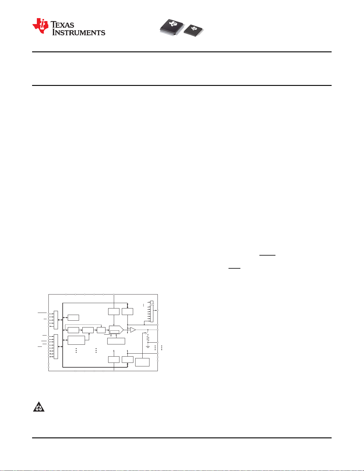
DESCRIPTION
The DAC7718 is a low-power, octal, 12-bit
digital-to-analog converter (DAC). With a 5V
reference, the output can either be a bipolar ±15V
voltage when operating from dual ±15.5V (or higher)
power supplies, or a unipolar 0V to +30V voltage
supply. With a 5.5V reference, the output can either
be a bipolar ±16.5V voltage when operating from dual
±17V (or higher) power supplies, or a unipolar 0V to
+33V voltage when operating from a +33.5V (or
higher) power supply. This DAC provides low-power
operation, good linearity, and low glitch over the
specified temperature range of –40°C to +105°C. This
device is trimmed in manufacturing and has very low
zero-code and gain error. In addition, system level
calibration can be performed over the entire signal
chain. The output range can be offset by using the
DAC offset register.
The DAC7718 features a standard, high-speed serial
peripheral interface (SPI) that operates at up to
50MHz and is 1.8V, 3V, and 5V logic compatible, to
communicate with a DSP or microprocessor. The
input data of the device are double-buffered. An
asynchronous load input (LDAC) transfers data from
the DAC data register to the DAC latch. The
asynchronous CLR input sets the output of all eight
DACs to AGND. The V
that connects to the individual analog outputs, the
offset DAC, the reference buffer outputs, and two
external inputs through a multiplexer (mux).
The DAC7718 is pin-to-pin and function-compatible
with the DAC8718 (16-bit) and the DAC8218 (14-bit).
pin is a monitor output
MON
1
2DSP is a trademark of Texas Instruments.
3SPI, QSPI are trademarks of Motorola Inc.
4Microwire is a trademark of National Semiconductor.
5All other trademarks are the property of their respective owners.
PRODUCTION DATA information is current as of publication date.
Products conform to specifications per the terms of the Texas
Instruments standard warranty. Production processing does not
necessarily include testing of allparameters.
Please be aware that an important notice concerning availability, standard warranty, and use in critical applications of Texas
Instruments semiconductor products and disclaimers thereto appears at the end of this data sheet.
Copyright © 2009, Texas Instruments Incorporated
DAC7718
SBAS361A –MAY 2009–REVISED DECEMBER 2009
www.ti.com
This integrated circuit can be damaged by ESD. Texas Instruments recommends that all integrated circuits be handled with
appropriate precautions. Failure to observe proper handling and installation procedures can cause damage.
ESD damage can range from subtle performance degradation to complete device failure. Precision integrated circuits may be more
susceptible to damage because very small parametric changes could cause the device not to meet its published specifications.
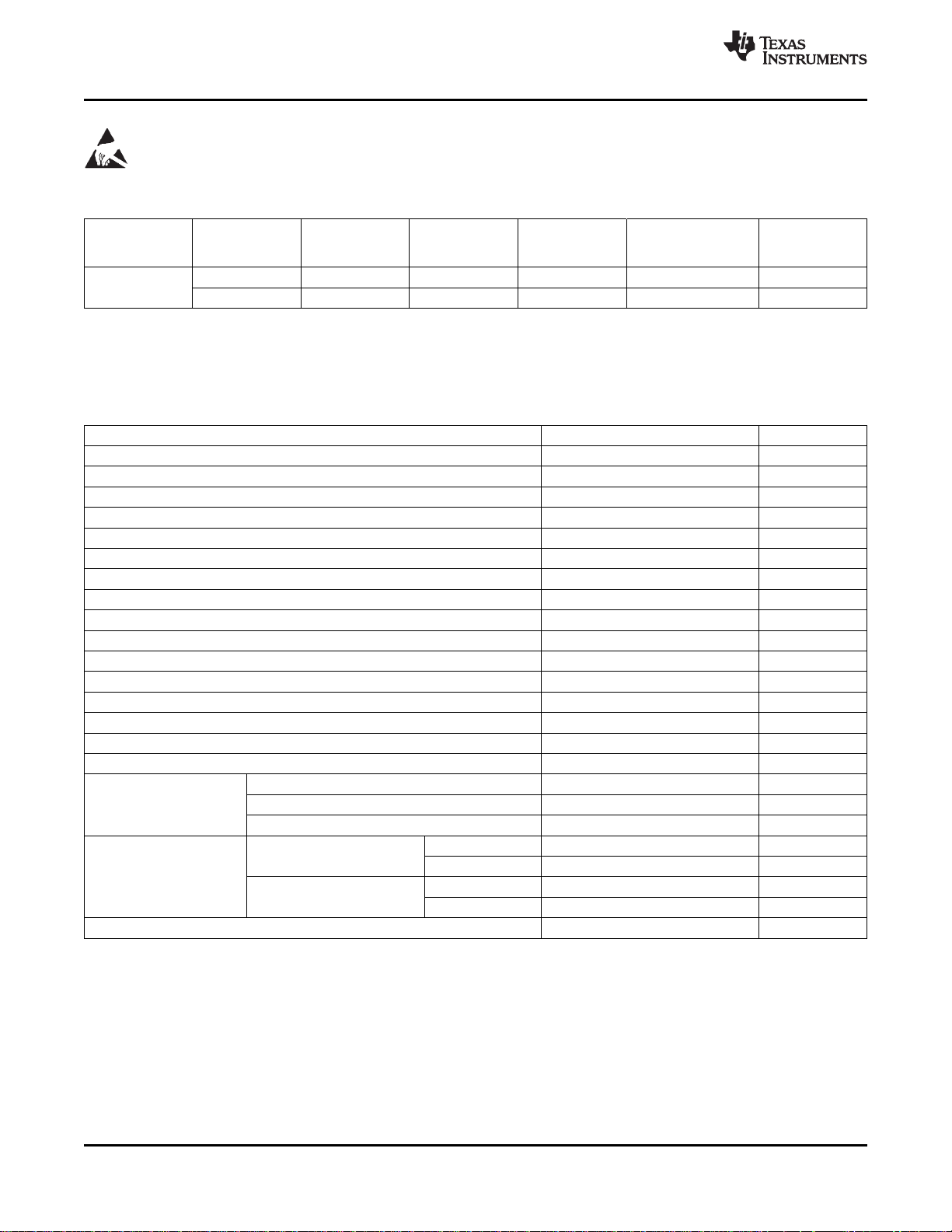
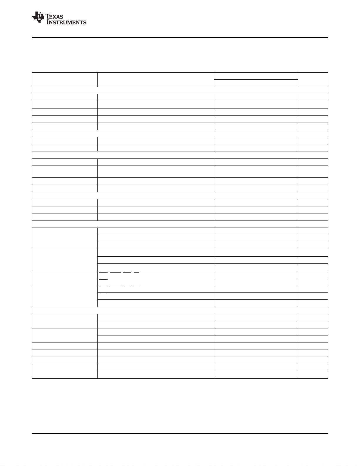
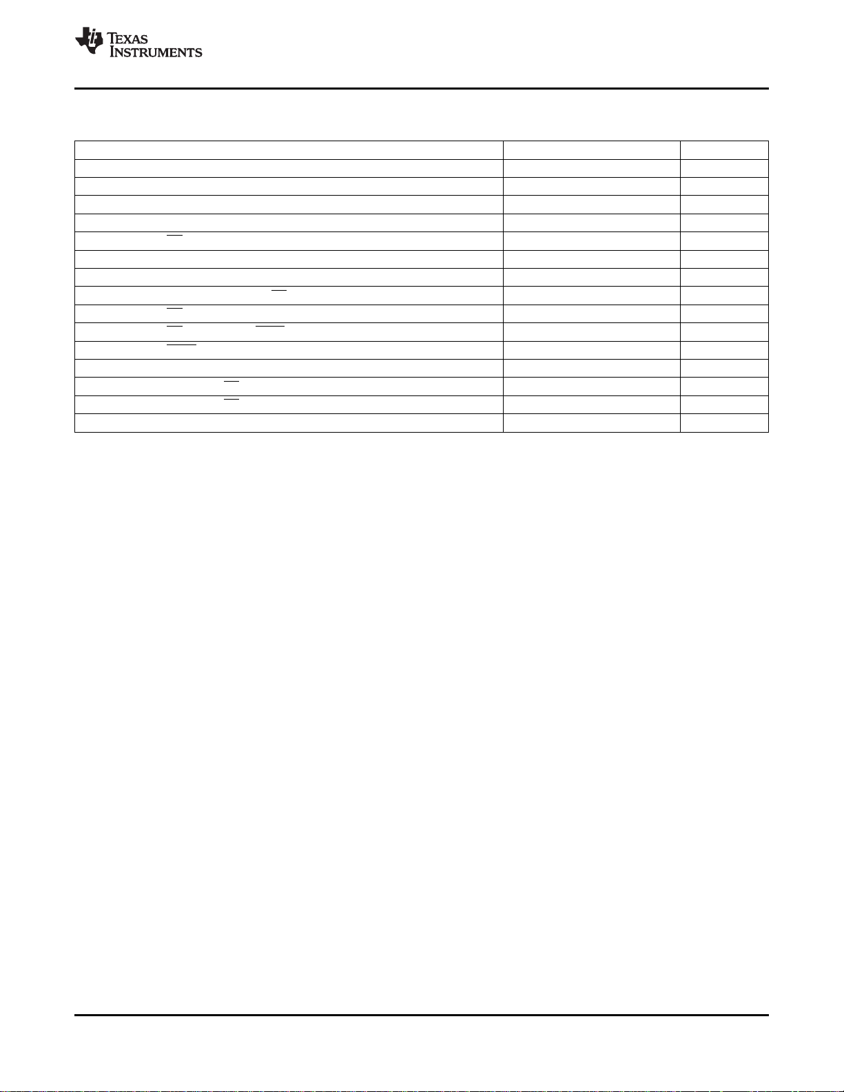
ORDERING INFORMATION
(1)
RELATIVE DIFFERENTIAL SPECIFIED
ACCURACY LINEARITY PACKAGE- PACKAGE TEMPERATURE PACKAGE
PRODUCT (LSB) (LSB) LEAD DESIGNATOR RANGE MARKING
DAC7718
±1 ±1 QFN-48 RGZ –40°C to +105°C DAC7718
±1 ±1 TQFP-64 PAG –40°C to +105°C DAC7718
(1) For the most current package and ordering information, see the Package Option Addendum at the end of this data sheet, or see the TI
web site at www.ti.com.
ABSOLUTE MAXIMUM RATINGS
(1)
Over operating free-air temperature range (unless otherwise noted).
DAC7718 UNIT
AVDDto AV
SS
AVDDto AGND –0.3 to 38 V
AVSSto AGND, DGND –19 to 0.3 V
DVDDto DGND –0.3 to 6 V
IOVDDto DGND –0.3 to min of (6 or DVDD+ 0.3) V
AGND-x to DGND –0.3 to 0.3 V
Digital input voltage to DGND –0.3 to IOVDD+ 0.3 V
SDO to DGND –0.3 to IOVDD+ 0.3 V
V
OUT
-x, V
, AIN-x to AV
MON
SS
REF-A, REF-B to AGND –0.3 to DV
GPIO-n to DGND –0.3 to IOVDD+ 0.3 V
GPIO-n input current 5 mA
Maximum current from V
MON
Operating temperature range –40 to +105 °C
Storage temperature range –65 to +150 °C
Maximum junction temperature (TJmax) +150 °C
Human body model (HBM) 2.5 kV
ESD ratings Charged device model (CDM) 1000 V
Machine model (MM) 200 V
TQFP 55 °C/W
QFN 27.5 °C/W
TQFP 21 °C/W
QFN 10.8 °C/W
Thermal impedance
Junction-to-ambient, q
Junction-to-case, q
JC
JA
Power dissipation (TJmax – TA) / q
(1) Stresses above those listed under Absolute Maximum Ratings may cause permanent damage to the device. Exposure to absolute
maximum conditions for extended periods may affect device reliability.
–0.3 to 38 V
–0.3 to AVDD+ 0.3 V
DD
3 mA
JA
V
W
2 Submit Documentation Feedback Copyright © 2009, Texas Instruments Incorporated
Product Folder Link(s): DAC7718
DAC7718
www.ti.com
SBAS361A –MAY 2009–REVISED DECEMBER 2009
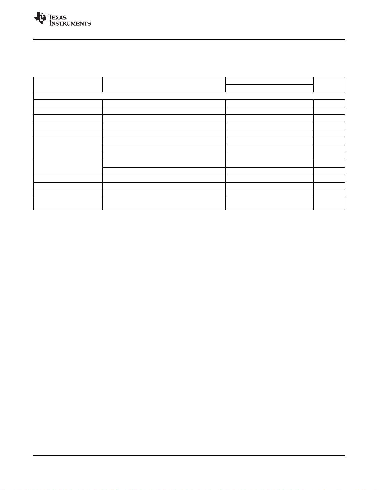
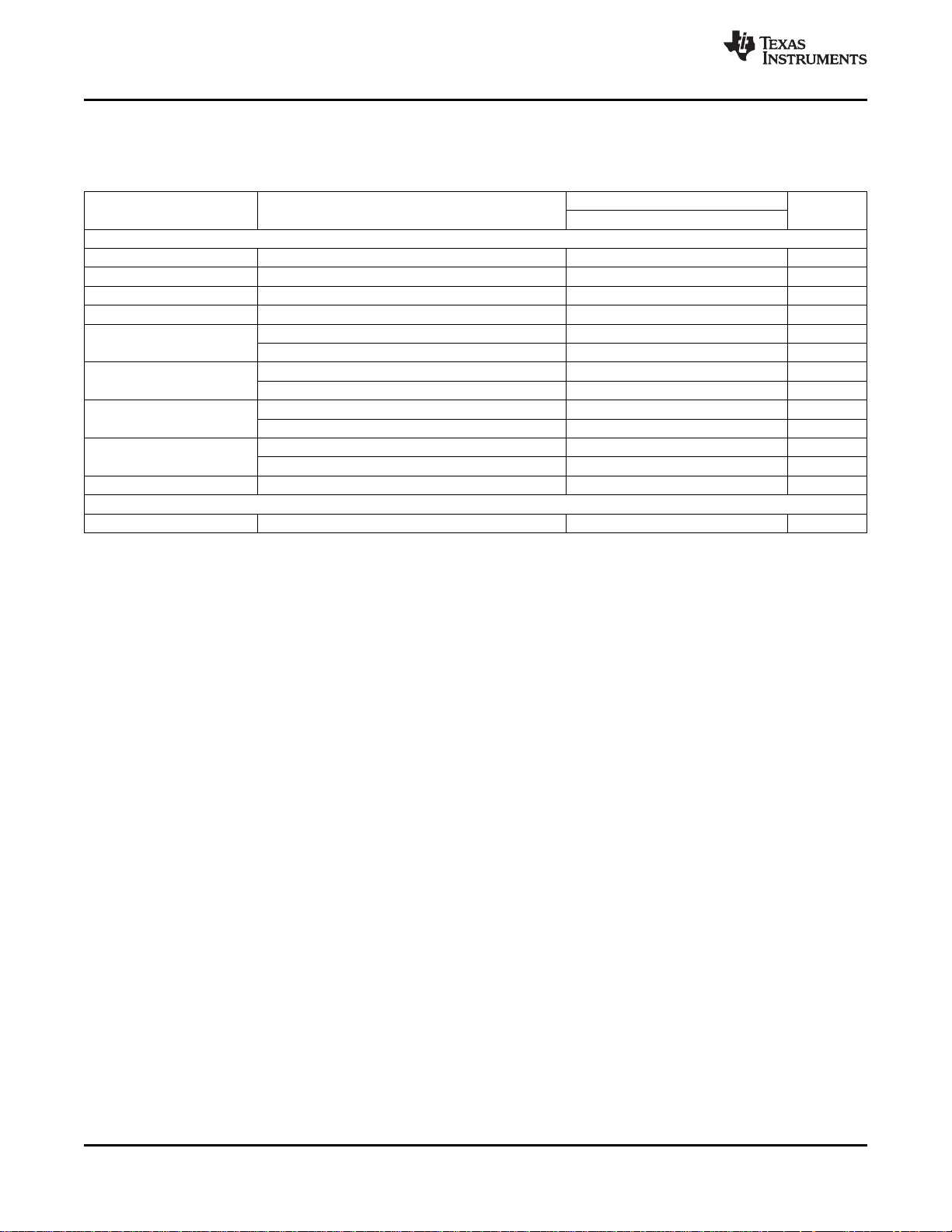
ELECTRICAL CHARACTERISTICS: Dual-Supply
All specifications at TA= T
gain = 6, AGND-x = DGND = 0V, data format = straight binary, and Offset DAC A and Offset DAC B are at default values
unless otherwise noted.
PARAMETER CONDITIONS MIN TYP MAX UNIT
STATIC PERFORMANCE
Resolution 12 Bits
Linearity error Measured by line passing through codes 000h and FFFh ±1 LSB
Differential linearity error Measured by line passing through codes 000h and FFFh ±1 LSB
Bipolar zero error TA= +25°C, gain = 4 or 6, code = 800h ±1 LSB
Bipolar zero error TC Gain = 4 or 6, code = 800h ±0.5 ±2 ppm FSR/°C
Zero-code error
Zero-code error TC Gain = 4 or 6, code = 000h ±0.5 ±3 ppm FSR/°C
Gain error
Gain error TC Gain = 4 or 6 ±1 ±3 ppm FSR/°C
Full-scale error TA= +25°C, gain = 4 or 6, code = FFFh ±1 LSB
Full-scale error TC Gain = 4 or 6, code = FFFh ±0.5 ±3 ppm FSR/°C
DC crosstalk
(3)
(1) Offset DAC A and Offset DAC B are trimmed in manufacturing to minimize the error for symmetrical output. The default value may vary
no more than ±1 LSB from the nominal number listed in Table 7. The Offset DAC pins are not intended to drive an external load, and
must not be connected during dual-supply operation.
(2) Gain = 4 and TC specified by design and characterization.
(3) The DAC outputs are buffered by op amps that share common AVDDand AVSSpower supplies. DC crosstalk indicates how much dc
change in one or more channel outputs may occur when the dc load current changes in one channel (because of an update). With
high-impedance loads, the effect is virtually immeasurable. Multiple AVDDand AVSSterminals are provided to minimize dc crosstalk.
(2)
to T
MIN
TA= +25°C, gain = 6, code = 000h ±1 LSB
TA= +25°C, gain = 4, code = 000h ±1 LSB
TA= +25°C, gain = 6 ±1 LSB
TA= +25°C, gain = 4 ±1 LSB
Measured channel at code = 800h, full-scale change on any
other channel
, AVDD= +16.5V, AVSS= –16.5V, IOVDD= DVDD= +5V, REF-A and REF-B = +5V,
MAX
DAC7718
0.05 LSB
(1)
,
Copyright © 2009, Texas Instruments Incorporated Submit Documentation Feedback 3
Product Folder Link(s): DAC7718
DAC7718
SBAS361A –MAY 2009–REVISED DECEMBER 2009
www.ti.com
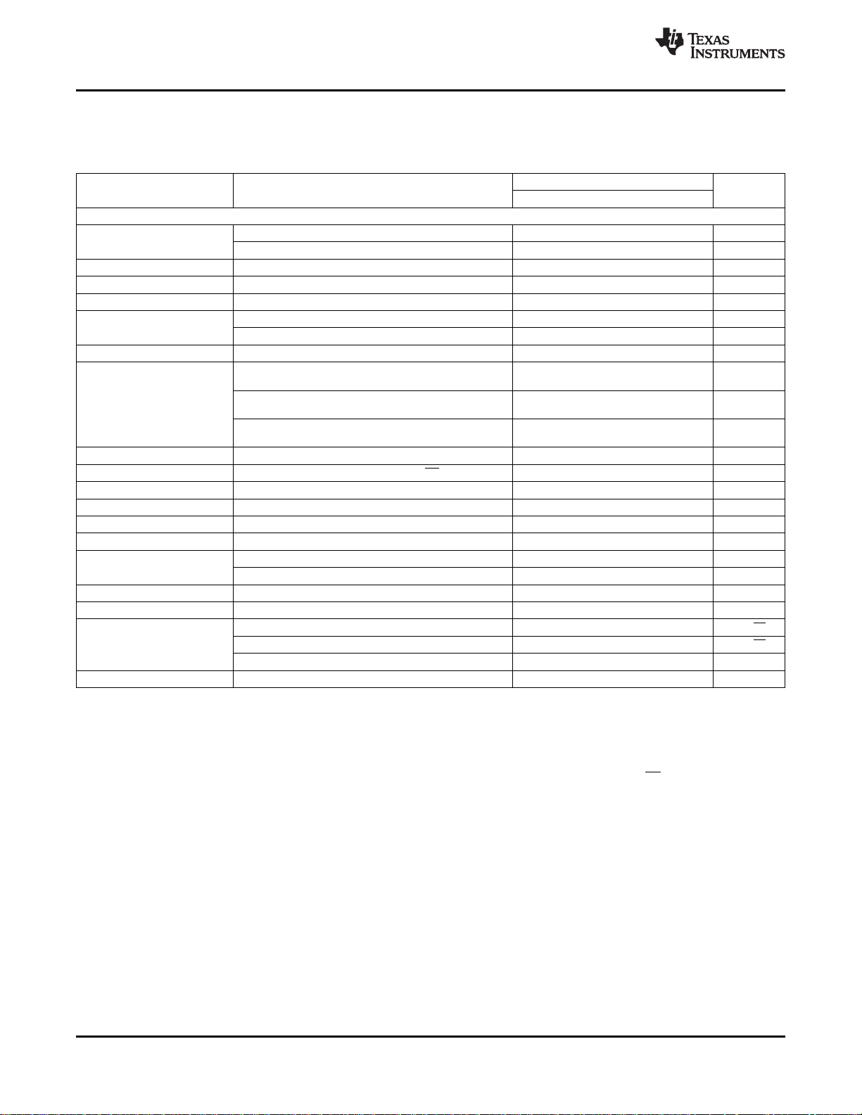
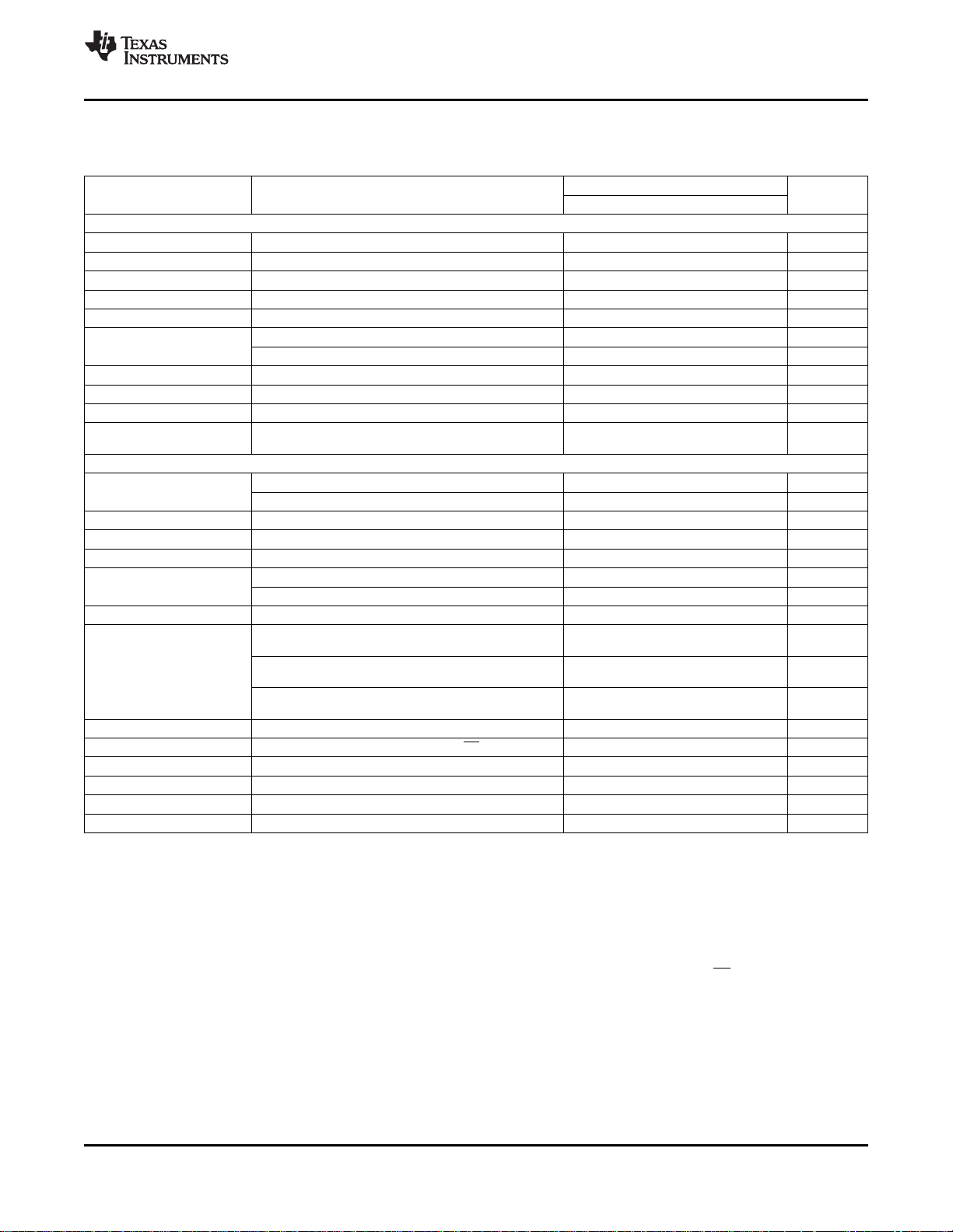
ELECTRICAL CHARACTERISTICS: Dual-Supply (continued)
All specifications at TA= T
gain = 6, AGND-x = DGND = 0V, data format = straight binary, and Offset DAC A and Offset DAC B are at default values
unless otherwise noted.
PARAMETER CONDITIONS MIN TYP MAX UNIT
ANALOG OUTPUT (V
Voltage output
Output impedance Code = 800h 0.5 Ω
Short-circuit current
Load current See Figure 37 ±3 mA
Output drift vs time
Capacitive load stability 500 pF
Settling time 15 ms
Slew rate
Power-on delay
Power-down recovery time 60 ms
Digital-to-analog glitch
Glitch impulse peak amplitude Code from 7FFh to 800h and 800h to 7FFh 5 mV
Channel-to-channel isolation
DAC-to-DAC crosstalk
Digital crosstalk
Digital feedthrough
Output noise TA= +25°C at 10kHz, gain = 4 130 nV/√Hz
Power-supply rejection
(5)
(7)
(8)
(12)
(4) Specified by design.
(5) The analog output range of V
the analog output must not be greater than (AVDD– 0.5V), and the minimum value must not be less than (AVSS+ 0.5V). All
specifications are for a ±16.5V power supply and a ±15V output, unless otherwise noted.
(6) When the output current is greater than the specification, the current is clamped at the specified maximum value.
(7) Slew rate is measured from 10% to 90% of the transition when the output changes from 0 to full-scale.
(8) Power-on delay is defined as the time from when the supply voltages reach the specified conditions to when CS goes low, for valid
digital communication.
(9) Digital-to-analog glitch is defined as the amount of energy injected into the analog output at the major code transition. It is specified as
the area of the glitch in nV-s. It is measured by toggling the DAC register data between 7FFh and 800h in straight binary format.
(10) Channel-to-channel isolation refers to the ratio of the signal amplitude at the output of one DAC channel to the amplitude of the
sinusoidal signal on the reference input of another DAC channel. It is expressed in dB and measured at midscale.
(11) DAC-to-DAC crosstalk is the glitch impulse that appears at the output of one DAC as a result of both the full-scale digital code and
subsequent analog output change at another DAC. It is measured with LDAC tied low and expressed in nV-s.
(12) Digital crosstalk is the glitch impulse transferred to the output of one converter as a result of a full-scale code change in the DAC input
register of another converter. It is measured when the DAC output is not updated, and is expressed in nV-s.
(13) Digital feedthrough is the glitch impulse injected to the output of a DAC as a result of a digital code change in the DAC input register of
the same DAC. It is measured with the full-scale digital code change without updating the DAC output, and is expressed in nV-s.
(14) The output must not be greater than (AVDD– 0.5V) and not less than (AVSS+ 0.5V).
(13)
-0 to V
OUT
(6)
(9)
(11)
(14)
to T
MIN
-7)
OUT
V
V
TA= +25°C, device operating for 500 hours, full-scale output 3.4 ppm of FSR
TA= +25°C, device operating for 1000 hours, full-scale output 4.3 ppm of FSR
To 0.03% of FSR, CL= 200pF, RL= 10kΩ, code from 000h to
FFFh and FFFh to 000h
To 1 LSB, CL= 200pF, RL= 10kΩ, code from 000h to FFFh
and FFFh to 000h
To 1 LSB, CL= 200pF, RL= 10kΩ, code from 7F0h to 810h
and 810h to 7F0h
From IOVDD≥ +1.8V and DVDD≥ +2.7V to CS low 200 ms
Code from 7FFh to 800h and 800h to 7FFh 4 nV-s
(10)
V
DACs in the same group 7.5 nV-s
DACs among different groups 1 nV-s
TA= +25°C at 10kHz, gain = 6 200 nV/√Hz
0.1Hz to 10Hz, gain = 6 20 mV
AVDD= ±15.5V to ±16.5V 0.05 LSB
, AVDD= +16.5V, AVSS= –16.5V, IOVDD= DVDD= +5V, REF-A and REF-B = +5V,
MAX
DAC7718
(4)
= +5V –15 +15 V
REF
= +1.5V –4.5 +4.5 V
REF
±8 mA
10 ms
6 ms
6 V/ms
= 4VPP, f = 1kHz 88 dB
REF
1 nV-s
1 nV-s
OUT
-0 to V
-7 is equal to (6 × V
OUT
– 5 × OUTPUT_OFFSET_DAC) for gain = 6. The maximum value of
REF
(1)
PP
,
4 Submit Documentation Feedback Copyright © 2009, Texas Instruments Incorporated
Product Folder Link(s): DAC7718
DAC7718
www.ti.com
SBAS361A –MAY 2009–REVISED DECEMBER 2009
ELECTRICAL CHARACTERISTICS: Dual-Supply (continued)
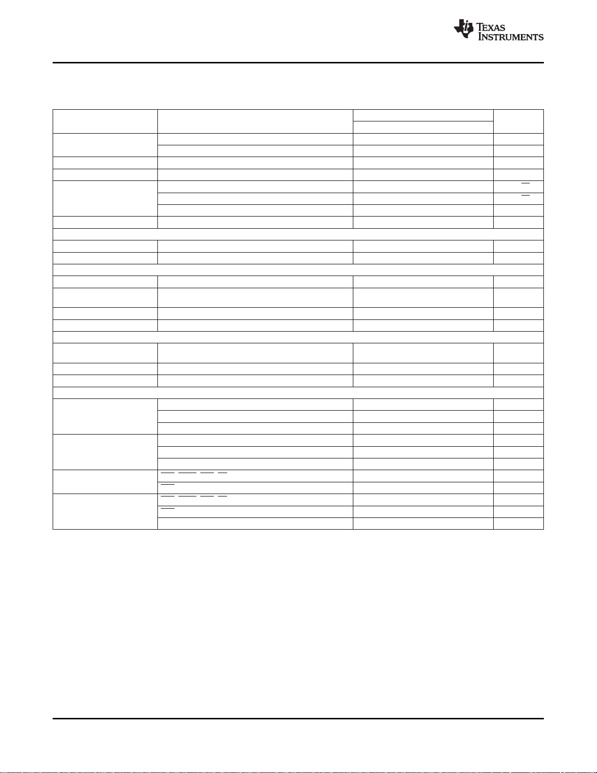
All specifications at TA= T
gain = 6, AGND-x = DGND = 0V, data format = straight binary, and Offset DAC A and Offset DAC B are at default values
unless otherwise noted.
PARAMETER CONDITIONS MIN TYP MAX UNIT
OFFSET DAC OUTPUT
Voltage output V
Full-scale error TA= +25°C ±0.25 LSB
Zero-code error TA= +25°C ±0.25 LSB
Linearity error ±0.5 LSB
Differential linearity error ±1 LSB
ANALOG MONITOR PIN (V
Output impedance
Three-state leakage current 100 nA
AUXILIARY ANALOG INPUT
Input range AV
Input impedance
(AIN-x to V
MON
)
Input capacitance
Input leakage current 30 nA
REFERENCE INPUT
Reference input voltage range
Reference input dc impedance 10 MΩ
Reference input capacitance
DIGITAL INPUT
High-level input voltage, V
Low-level input voltage, V
Input current
Input capacitance USB/BTC and RSTSEL 12 pF
DIGITAL OUTPUT
High-level output voltage, V
(SDO)
Low-level output voltage, V
(SDO)
GPIO-n output voltage low, V
GPIO-n output voltage high, VOH10kΩ pull-up resistor to IOV
High-impedance leakage current SDO and GPIO-n ±5 mA
High-impedance output
capacitance
(15) Specified by design.
(16) Offset DAC A and Offset DAC B are trimmed in manufacturing to minimize the error for symmetrical output. The default value may vary
no more than ±1 LSB from the nominal number listed in Table 7. The Offset DAC pins are not intended to drive an external load, and
must not be connected during dual-supply operation.
(17) 8kΩ when V
(18) Reference input voltage ≤ DVDD.
(15) (16)
(17)
(15)
(15)
IH
IL
(15)
OH
OL
is connected to Reference Buffer A or B, and 4kΩ when V
MON
to T
MIN
, AVDD= +16.5V, AVSS= –16.5V, IOVDD= DVDD= +5V, REF-A and REF-B = +5V,
MAX
DAC7718
= +5V 0 5 V
REF
)
MON
TA= +25°C 2 kΩ
SS
TA= +25°C 2 kΩ
4 pF
(18)
(15)
1.0 5.5 V
10 pF
IOVDD= +4.5V to +5.5V 3.8 0.3 + IOV
IOVDD= +2.7V to +3.3V 2.3 0.3 + IOV
IOVDD= +1.7V to 2.0V 1.5 0.3 + IOV
IOVDD= +4.5V to +5.5V –0.3 0.8 V
IOVDD= +2.7V to +3.3V –0.3 0.6 V
IOVDD= +1.7V to 2.0V –0.3 0.3 V
CLR, LDAC, RST, CS, and SDI ±1 mA
USB/BTC, RSTSEL, and GPIO-n ±5 mA
CLR, LDAC, RST, CS, and SDI 5 pF
GPIO-n 14 pF
IOVDD= +2.7V to +5.5V, sourcing 1mA IOVDD– 0.4 IOV
IOVDD= +1.8V, sourcing 200mA 1.6 IOV
IOVDD= +2.7V to +5.5V, sinking 1mA 0 0.4 V
IOVDD= +1.8V, sinking 200mA 0 0.2 V
1mA sink from IOV
OL
DD
DD
0.99 × IOV
DD
0.15 V
SDO 5 pF
GPIO-n 14 pF
is connected to Offset DAC-A or -B.
MON
AV
(1)
DD
DD
DD
DD
DD
DD
V
V
V
V
V
V
V
,
Copyright © 2009, Texas Instruments Incorporated Submit Documentation Feedback 5
Product Folder Link(s): DAC7718
DAC7718
SBAS361A –MAY 2009–REVISED DECEMBER 2009
www.ti.com
ELECTRICAL CHARACTERISTICS: Dual-Supply (continued)
All specifications at TA= T
gain = 6, AGND-x = DGND = 0V, data format = straight binary, and Offset DAC A and Offset DAC B are at default values
unless otherwise noted.
PARAMETER CONDITIONS MIN TYP MAX UNIT
POWER SUPPLY
AV
DD
AV
SS
DV
DD
(19)
IOV
DD
AI
DD
AI
SS
DI
DD
IOI
DD
Power dissipation Normal operation, ±16.5V supplies, midscale code 115 165 mW
TEMPERATURE RANGE
Specified performance –40 +105 °C
(19) IOVDD≤ DVDD.
to T
MIN
Normal operation, midscale code, output unloaded 4.3 6 mA
Power down, output unloaded 35 mA
Normal operation, midscale code, output unloaded –4 –2.7 mA
Power down, output unloaded 35 mA
Normal operation 78 mA
Power down 36 mA
Normal operation, VIH= IOVDD, VIL= DGND 5 mA
Power down, VIH= IOVDD, VIL= DGND 5 mA
, AVDD= +16.5V, AVSS= –16.5V, IOVDD= DVDD= +5V, REF-A and REF-B = +5V,
MAX
DAC7718
+4.5 +18 V
–18 –4.5 V
+2.7 +5.5 V
+1.8 +5.5 V
(1)
,
6 Submit Documentation Feedback Copyright © 2009, Texas Instruments Incorporated
Product Folder Link(s): DAC7718
DAC7718
www.ti.com
SBAS361A –MAY 2009–REVISED DECEMBER 2009
ELECTRICAL CHARACTERISTICS: Single-Supply
All specifications at TA= T
AGND-x = DGND = 0V, data format = straight binary, and OFFSET-A = OFFSET-B = AGND, unless otherwise noted.
PARAMETER CONDITIONS MIN TYP MAX UNIT
STATIC PERFORMANCE
Resolution 12 Bits
Linearity error Measured by line passing through codes 010h and FFFh ±1 LSB
Differential linearity error Measured by line passing through codes 010h and FFFh ±1 LSB
Unipolar zero error TA= +25°C, gain = 4 or 6, code = 010h ±1 LSB
Unipolar zero error TC Gain = 4 or 6, code = 010h ±0.5 ±3 ppm FSR/°C
Gain error
Gain error TC Gain = 4 or 6 ±1 ±3 ppm FSR/°C
Full-scale error TA= +25°C, gain = 4 or 6, code = FFFh ±1 LSB
Full-scale error TC Gain = 4 or 6, code = FFFh ±0.5 ±3 ppm FSR/°C
DC crosstalk
ANALOG OUTPUT (V
Voltage output
Output impedance Code = 800h 0.5 Ω
Short-circuit current
Load current SeeFigure 84 and Figure 85 ±3 mA
Output drift vs time
Capacitive load stability 500 pF
Settling time 15 ms
Slew rate
Power-on delay
Power-down recovery time 90 ms
Digital-to-analog glitch
Glitch impulse peak amplitude Code from 7FFh to 800h and 800h to 7FFh 5 mV
Channel-to-channel isolation
(2)
(4)
(6)
(7)
(1) Gain = 4 and TC specified by design and characterization.
(2) The DAC outputs are buffered by op amps that share common AVDDand AVSSpower supplies. DC crosstalk indicates how much dc
change in one or more channel outputs may occur when the dc load current changes in one channel (because of an update). With
high-impedance loads, the effect is virtually immeasurable. Multiple AVDDand AVSSterminals are provided to minimize dc crosstalk.
(3) Specified by design.
(4) The analog output range of V
greater than (AVDD– 0.5V). All specifications are for a +32V power supply and a 0V to +30V output, unless otherwise noted.
(5) When the output current is greater than the specification, the current is clamped at the specified maximum value.
(6) Slew rate is measured from 10% to 90% of the transition when the output changes from 0 to full-scale.
(7) Power-on delay is defined as the time from when the supply voltages reach the specified conditions to when CS goes low, for valid
digital communication.
(8) Digital-to-analog glitch is defined as the amount of energy injected into the analog output at the major code transition. It is specified as
the area of the glitch in nV-s. It is measured by toggling the DAC register data between 7FFh and 800h in straight binary format.
(9) Channel-to-channel isolation refers to the ratio of the signal amplitude at the output of one DAC channel to the amplitude of the
sinusoidal signal on the reference input of another DAC channel. It is expressed in dB and measured at midscale.
(1)
-0 to V
OUT
(5)
(8)
to T
MIN
TA= +25°C, gain = 6 ±1 LSB
TA= +25°C, gain = 4 ±1 LSB
Measured channel at code = 800h, full-scale change on any
other channel
-7)
OUT
V
REF
V
REF
TA= +25°C, device operating for 500 hours, full-scale output 3.4 ppm of FSR
TA= +25°C, device operating for 1000 hours, full-scale output 4.3 ppm of FSR
To 0.03% of FSR, CL= 200pF, RL= 10kΩ, code from 010h to
FFFh and FFFh to 010h
To 1 LSB, CL= 200pF, RL= 10kΩ, code from 010h to FFFh
and FFFh to 010h
To 1 LSB, CL= 200pF, RL= 10kΩ, code from 7F0h to 810h
and 810h to 7F0h
From IOVDD≥ +1.8V and DVDD≥ +2.7V to CS low 200 ms
Code from 7FFh to 800h and 800h to 7FFh 4 nV-s
(9)
V
REF
, AVDD= +32V, AVSS= 0V, IOVDD= DVDD= +5V, REF-A and REF-B = +5V, gain = 6,
MAX
DAC7718
0.05 LSB
(3)
= +5V 0 +30 V
= +1.5V 0 +9 V
±8 mA
10 ms
6 ms
6 V/ms
= 4VPP, f = 1kHz 88 dB
OUT
-0 to V
-7 is equal to (6 × V
OUT
) for gain = 6. The maximum value of the analog output must not be
REF
Copyright © 2009, Texas Instruments Incorporated Submit Documentation Feedback 7
Product Folder Link(s): DAC7718
DAC7718
SBAS361A –MAY 2009–REVISED DECEMBER 2009
www.ti.com
ELECTRICAL CHARACTERISTICS: Single-Supply (continued)
All specifications at TA= T
AGND-x = DGND = 0V, data format = straight binary, and OFFSET-A = OFFSET-B = AGND, unless otherwise noted.
PARAMETER CONDITIONS MIN TYP MAX UNIT
DAC-to-DAC crosstalk
Digital crosstalk
Digital feedthrough
Output noise TA= +25°C at 10kHz, gain = 4 130 nV/√Hz
Power-supply rejection
ANALOG MONITOR PIN (V
Output impedance
Three-state leakage current 100 nA
AUXILIARY ANALOG INPUT
Input range AV
Input impedance
(AIN-x to V
MON
Input capacitance
Input leakage current 30 nA
REFERENCE INPUT
Reference input voltage
(16)
range
Reference input dc impedance 10 MΩ
Reference input capacitance
DIGITAL INPUT
High-level input voltage, V
Low-level input voltage, V
Input current
Input capacitance USB/BTC and RSTSEL 12 pF
(10) DAC-to-DAC crosstalk is the glitch impulse that appears at the output of one DAC as a result of both the full-scale digital code and
subsequent analog output change at another DAC. It is measured with LDAC tied low and expressed in nV-s.
(11) Digital crosstalk is the glitch impulse transferred to the output of one converter as a result of a full-scale code change in the DAC input
register of another converter. It is measured when the DAC output is not updated, and is expressed in nV-s.
(12) Digital feedthrough is the glitch impulse injected to the output of a DAC as a result of a digital code change in the DAC input register of
the same DAC. It is measured with the full-scale digital code change without updating the DAC output, and is expressed in nV-s.
(13) The analog output must not be greater than (AVDD– 0.5V).
(14) 8kΩ when V
(15) Specified by design.
(16) Reference input voltage ≤ DVDD.
(10)
(11)
(12)
(13)
(14)
)
(15)
(15)
IH
IL
is connected to Reference Buffer A or B, and 4kΩ when V
MON
to T
MIN
, AVDD= +32V, AVSS= 0V, IOVDD= DVDD= +5V, REF-A and REF-B = +5V, gain = 6,
MAX
DAC7718
DACs in the same group 10 nV-s
DACs among different groups 1 nV-s
1 nV-s
1 nV-s
TA= +25°C at 10kHz, gain = 6 200 nV/√Hz
0.1Hz to 10Hz, gain = 6 20 mV
AVDD= +33V to +36V 0.05 LSB
)
MON
TA= +25°C 2 kΩ
SS
AV
DD
TA= +25°C 2 kΩ
4 pF
1.0 5.5 V
(15)
IOVDD= +4.5V to +5.5V 3.8 0.3 + IOV
IOVDD= +2.7V to +3.3V 2.3 0.3 + IOV
IOVDD= +1.7V to 2.0V 1.5 0.3 + IOV
10 pF
DD
DD
DD
IOVDD= +4.5V to +5.5V –0.3 0.8 V
IOVDD= +2.7V to +3.3V –0.3 0.6 V
IOVDD= +1.7V to 2.0V –0.3 0.3 V
CLR, LDAC, RST, CS, and SDI ±1 mA
USB/BTC, RSTSEL, and GPIO-n ±5 mA
CLR, LDAC, RST, CS, and SDI 5 pF
GPIO-n 14 pF
is connected to Offset DAC-A or -B.
MON
PP
V
V
V
V
8 Submit Documentation Feedback Copyright © 2009, Texas Instruments Incorporated
Product Folder Link(s): DAC7718
DAC7718
www.ti.com
SBAS361A –MAY 2009–REVISED DECEMBER 2009
ELECTRICAL CHARACTERISTICS: Single-Supply (continued)
All specifications at TA= T
AGND-x = DGND = 0V, data format = straight binary, and OFFSET-A = OFFSET-B = AGND, unless otherwise noted.
PARAMETER CONDITIONS MIN TYP MAX UNIT
DIGITAL OUTPUT
High-level output voltage, V
(SDO)
Low-level output voltage, V
(SDO)
GPIO-n output voltage low, VOL1mA sink from IOV
GPIO-n output voltage high, VOH10kΩ pull-up resistor to IOV
High-impedance leakage current SDO and GPIO-n ±5 mA
High-impedance output
capacitance
POWER SUPPLY
AV
DD
DV
DD
(18)
IOV
DD
AI
DD
DI
DD
IOI
DD
Power dissipation Normal operation 140 225 mW
TEMPERATURE RANGE
Specified performance –40 +105 °C
(17) Specified by design.
(18) IOVDD≤ DVDD.
(17)
OH
OL
to T
MIN
, AVDD= +32V, AVSS= 0V, IOVDD= DVDD= +5V, REF-A and REF-B = +5V, gain = 6,
MAX
DAC7718
IOVDD= +2.7V to +5.5V, sourcing 1mA IOVDD– 0.4 IOV
IOVDD= +1.8V, sourcing 200mA 1.6 IOV
DD
DD
IOVDD= +2.7V to +5.5V, sinking 1mA 0 0.4 V
IOVDD= +1.8V, sinking 200mA 0 0.2 V
DD
DD
0.99 × IOV
DD
0.15 V
SDO 5 pF
GPIO-n 14 pF
+9 +36 V
+2.7 +5.5 V
+1.8 +5.5 V
Normal operation, midscale code, output unloaded 4.5 7 mA
Power down, output unloaded 35 µA
Normal operation 70 mA
Power down 36 mA
Normal operation, VIH= IOVDD, VIL= DGND 5 mA
Power down, VIH= IOVDD, VIL= DGND 5 mA
V
V
V
Copyright © 2009, Texas Instruments Incorporated Submit Documentation Feedback 9
Product Folder Link(s): DAC7718
ControlLogic
An ogal Monit ro
ToDAC-0,DAC-1,
DAC-2,DAC-3
ToDAC-0,DAC-1,
DAC-2,DAC-3
ToDAC-4,DAC-5,DAC-6,DAC-7
DAC7718
OFFSET-B
AGND-B
V -7
OUT
V
MON
OFFSET-A
AGND-A
REF-B
Reference
BufferB
InternalTrimming
Zero/Gain;INL
Reference
BufferA
OFFSET
DACA
OFFSET
DACB
DAC-0
Latch-0
Power-Up/
Power-Down
Control
(SameFunctionBlocks
forAllChannels)
REF-A
LDAC
RST
RSTSEL
LDAC
CLR
USB/BTC
AIN-0
AIN-1
GPIO-0
GPIO-1
GPIO-2
SDO
SDI
CS
SCLK
WAKEUP
SPIShiftRegister
IOVDDDGND DV
DD
AV
DD
AV
SS
DGND DV
DD
AV
DD
AV
SS
V -0
OUT
V -7
OUT
AIN-0
AIN-1
RefBufferA
RefBufferB
OFFSET-B
Mux
Command
Registers
InputData
Register0
Correction
Engine
(WhenCorrectionEngineDisabled)
DAC-0
Data
UserCalibration:
ZeroRegister0
GainRegsiter0
V -0
OUT
DAC7718
SBAS361A –MAY 2009–REVISED DECEMBER 2009
www.ti.com
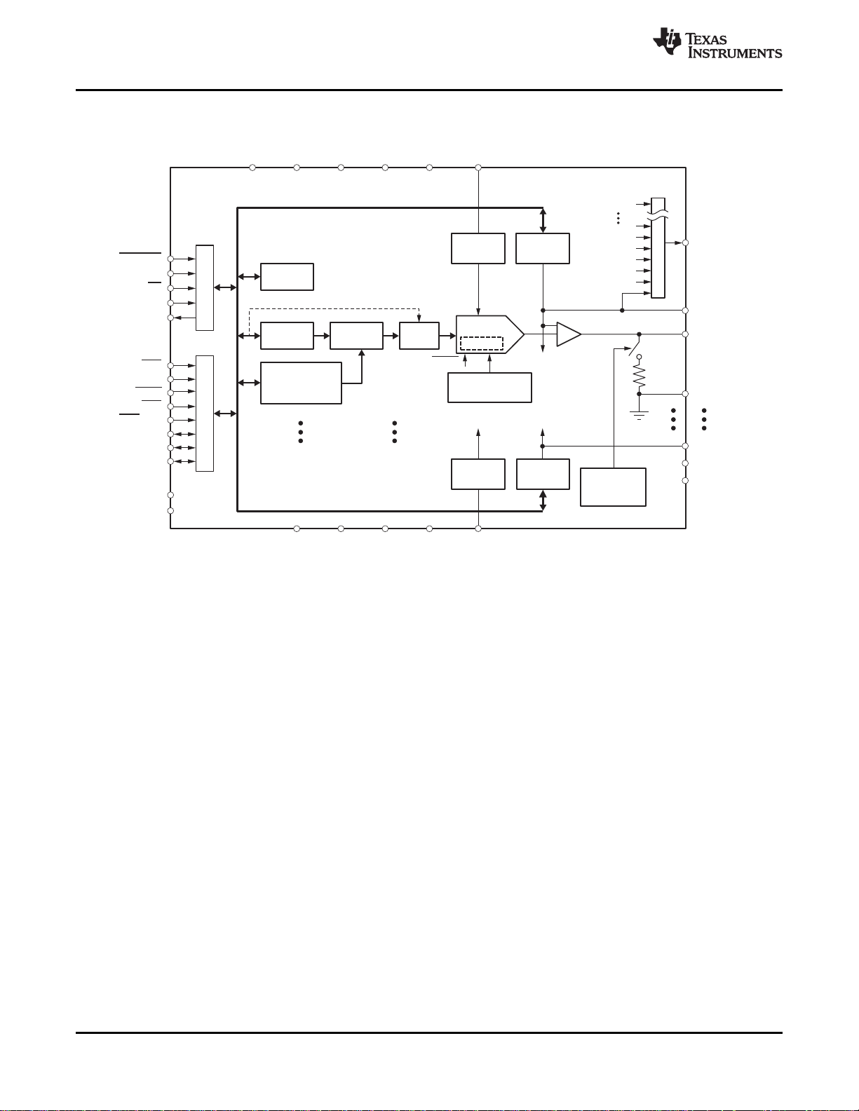
FUNCTIONAL BLOCK DIAGRAM
Figure 1. Functional Block Diagram
10 Submit Documentation Feedback Copyright © 2009, Texas Instruments Incorporated
Product Folder Link(s): DAC7718
48
47
46
45
44
43
42
41
40
39
38
37
36
35
34
33
AV
DD
NC
AIN-1
V -4
OUT
REF-B
V -5
OUT
V -6
OUT
AGND-B
AGND-B
OFFSET-B
V -7
OUT
AV
SS
NC
NC
NC
NC
1
2
3
4
5
6
7
8
9
10
11
12
13
14
15
16
AV
DD
NC
AIN-0
V -3
OUT
REF-A
V -2
OUT
V -1
OUT
AGND-A
AGND-A
OFFSET-A
V -0
OUT
AV
SS
NC
V
MON
NC
NC
NC
WAKEUP
LDAC
SDONCSDICSSCLK
DV
DD
IOV
DD
DGNDNCNC
RSTSEL
USB/BTC
NC
NC
NC
GPIO-2
CLR
RST
NC
NC
DV
DD
DGND
NC
NC
DGND
GPIO-1
GPIO-0
NC
NC
64 63 62 61 60 59 58 57 56 55 54
17
18 19 20
21 222324
25 26
27
53 52 51 50 49
28 29 30 31 32
DAC7718
AV
DD
AIN-0
V -3
OUT
REF-A
V -2
OUT
V -1
OUT
AGND-A
AGND-A
OFFSET-A
V -0
OUT
AV
SS
V
MON
AV
DD
AIN-1
V -4
OUT
REF-B
V -5
OUT
V -6
OUT
AGND-B
AGND-B
OFFSET-B
V -7
OUT
AV
SS
NC
1
2
3
4
5
6
7
8
9
10
11
12
36
35
34
33
32
31
30
29
28
27
26
25
DAC7718
WAKEUP
LDAC
SDO
SDICSSCLK
DV
DD
IOV
DD
DGNDNCRSTSEL
USB/BTC
4847464544434241403938
37
GPIO-2
CLR
RST
NC
DV
DD
NC
NC
DGND
NC
DGND
GPIO-1
GPIO-0
1314151617181920212223
24
DAC7718
www.ti.com
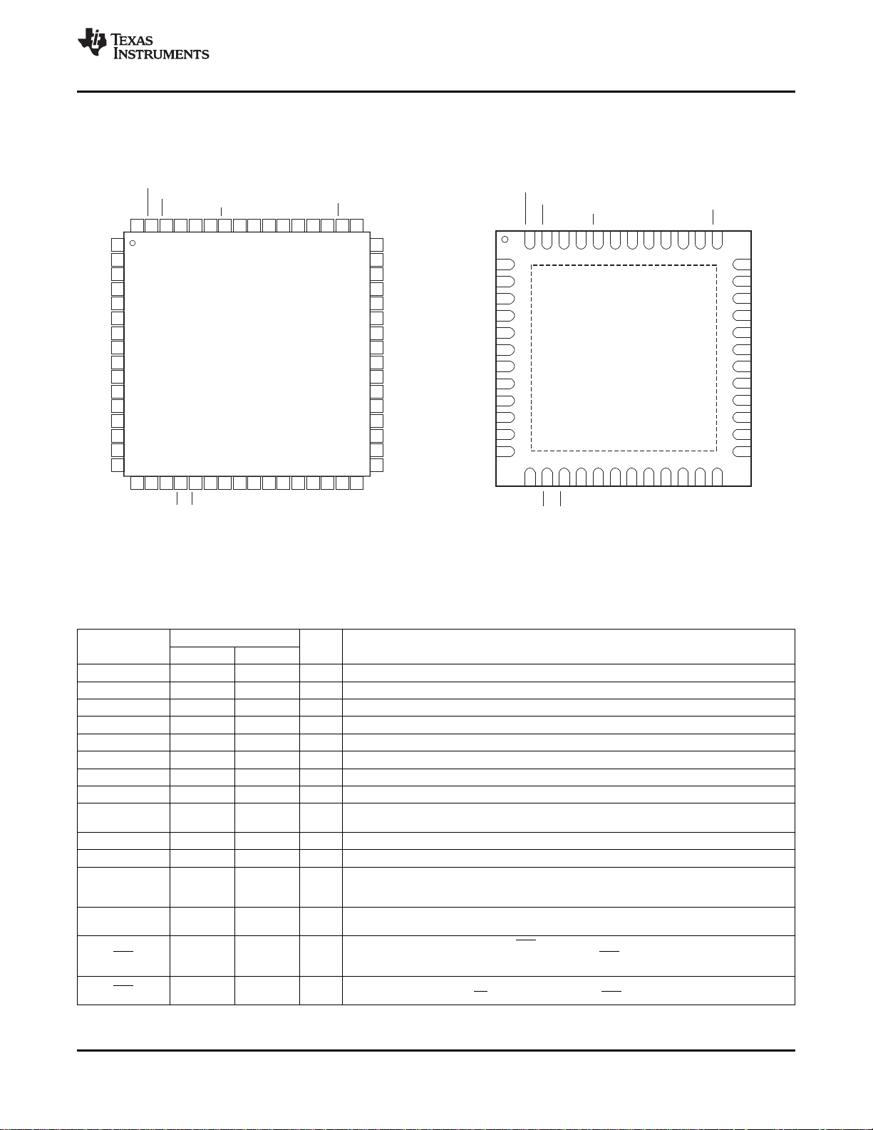
PAG PACKAGE
TQFP-64
(TOP VIEW)
SBAS361A –MAY 2009–REVISED DECEMBER 2009
PIN CONFIGURATIONS
RGZ PACKAGE
QFN-48
(TOP VIEW)
PIN
NAME
AV
DD
AIN-0 2 3 I Auxiliary analog input 0, directly routed to the analog mux
V
-3 3 4 O DAC-3 output
OUT
REF-A 4 5 I Group A
V
-2 5 6 O DAC-2 output
OUT
V
-1 6 7 O DAC-1 output
OUT
AGND-A 7 8 I Group A analog ground and the ground of REF-A. This pin must be tied to AGND-B and DGND.
AGND-A 8 9 I Group A analog ground and the ground of REF-A. This pin must be tied to AGND-B and DGND.
OFFSET-A 9 10 O
(1) Group A consists of DAC-0, DAC-1, DAC-2, and DAC-3. Group B consists of DAC-4, DAC-5, DAC-6, and DAC-7.
Copyright © 2009, Texas Instruments Incorporated Submit Documentation Feedback 11
V
-0 10 11 O DAC-0 output
OUT
AV
SS
V
MON
GPIO-2 13 19 I/O
CLR 14 20 I through switches and internal low-impedance. When the CLR pin is logic '1', all V
RST 15 21 I
(1) The thermal pad is internally connected to
the substrate. This pad can be connected
to AVSSor left floating. Keep the thermal
pad separate from the digital ground, if
possible.
PIN DESCRIPTIONS
PIN NO.
QFN-48 TQFP-64 I/O DESCRIPTION
1 1 I Positive analog power supply
(1)
reference input
11 12 I Negative analog power supply
12 14 O reference buffer outputs, offset DAC outputs, or one of the auxiliary analog inputs, depending on
OFFSET DAC-A analog output. Must be connected to AGND-A during single power-supply
operation (AVSS= 0V). This pin is not intended to drive an external load.
Analog monitor output. This pin is either in Hi-Z status, connected to one of the eight DAC outputs,
the content of the Monitor Register. See the Monitor Register, Table 12, for details.
General-purpose digital input/output 2. This pin is a bidirectional digital input/output, open-drain and
requires an external pull-up resistor. See the GPIO Pins section for details.
Clear input, level triggered. When the CLR pin is logic '0', all V
connect to the amplifier outputs.
Reset input (active low). Logic low on this pin resets the DAC registers and DACs to the values
defined by the RSTSEL pin. CS must be logic high when RST is active.
Product Folder Link(s): DAC7718
-X pins connect to AGND-x
OUT
OUT
-X pins
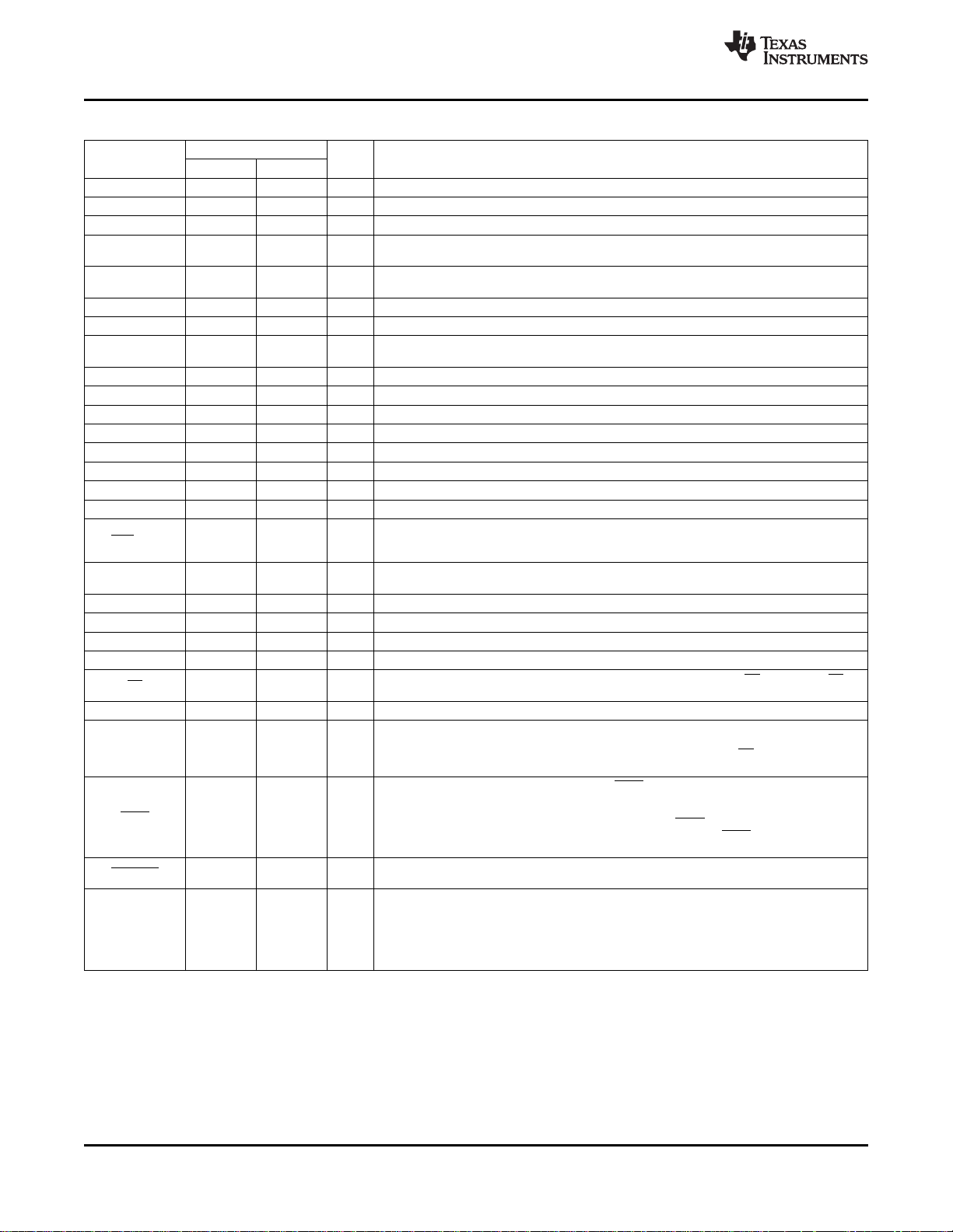
DAC7718
SBAS361A –MAY 2009–REVISED DECEMBER 2009
PIN DESCRIPTIONS (continued)
PIN
NAME
DV
DD
DGND 20 25 I Digital ground
DGND 22 28 I Digital ground
GPIO-1 23 29 I/O
GPIO-0 24 30 I/O
AV
SS
V
-7 27 38 O DAC-7 output
OUT
OFFSET-B 28 39 O
AGND-B 29 40 I Group B
AGND-B 30 41 I Group B analog ground and the ground of REF-B. This pin must be tied to AGND-A and DGND.
V
-6 31 42 O DAC-6 output
OUT
V
-5 32 43 O DAC-5 output
OUT
REF-B 33 44 I Group B reference input
V
-4 34 45 O DAC-4 output
OUT
AIN-1 35 46 I Auxiliary analog input 1, directly routed to the analog mux
AV
DD
USB/BTC 37 50 I when connected to DGND or in twos complement format when connected to IOVDD. The command
RSTSEL 38 51 I
DGND 40 54 I Digital ground
IOV
DD
DV
DD
SCLK 43 57 I SPI bus serial clock input
CS 44 58 I
SDI 45 59 I SPI bus serial data input
SDO 46 61 O
LDAC 47 62 I
WAKEUP 48 63 I
NC — Not connected
PIN NO.
QFN-48 TQFP-64 I/O DESCRIPTION
17 24 I Digital power supply
General-purpose digital input/output 1. This pin is a bidirectional digital input/output, open-drain and
requires an external resistor. See the GPIO Pins section for details.
General-purpose digital input/output 0. This pin is a bidirectional digital input/output, open-drain and
requires an external resistor. See the GPIO Pins section for details.
26 37 I Negative analog power supply
OFFSET DAC-B analog output. Must be connected to AGND-B during single-supply operation
(AVSS= 0V).
(1)
analog ground and the ground of REF-B. This pin must be tied to AGND-A and DGND.
36 48 I Positive analog power supply
Data format selection of Input DAC data and Offset DAC data. Data are in straight binary format
data are always in straight binary format. Refer to Input Data Format section for details.
Output reset selection. Selects the output voltage on the V
Refer to the Power-On Reset section for details.
41 55 I Interface power
42 56 I Digital power supply
SPI bus chip select input (active low). Data are not clocked into SDI unless CS is low. When CS is
high, SDO is in a high-impedance state and the SCLK and SDI signals are blocked from the device.
SPI bus serial data output.
When the DSDO bit = '0', the SDO pin works as an output in normal operation.
When the DSDO bit = '1', SDO is always in a Hi-Z state, regardless of the CS pin status. Refer to
the Timing Diagrams section for details.
Load DAC latch control input (active low). When LDAC is low, the DAC latch is transparent and the
contents of the DAC Data Register are transferred to it. The DAC output changes to the
corresponding level simultaneously when the DAC latch is updated. See the Updating the DAC
Outputs section for details. If asynchronous mode is desired, LDAC must be permanently tied low
before power is applied to the device. If synchronous mode is desired, LDAC must be logic high
during power-on.
Wake-up input (active low). Restores the SPI from sleep to normal operation. See the Daisy-Chain
Operation section for details.
2, 13,
15-18, 22,
16, 18, 19, 23, 26, 27,
21, 25, 39 31-36, 47,
49, 52, 53,
60, 64
pin after power-on or hardware reset.
OUT
www.ti.com
12 Submit Documentation Feedback Copyright © 2009, Texas Instruments Incorporated
Product Folder Link(s): DAC7718
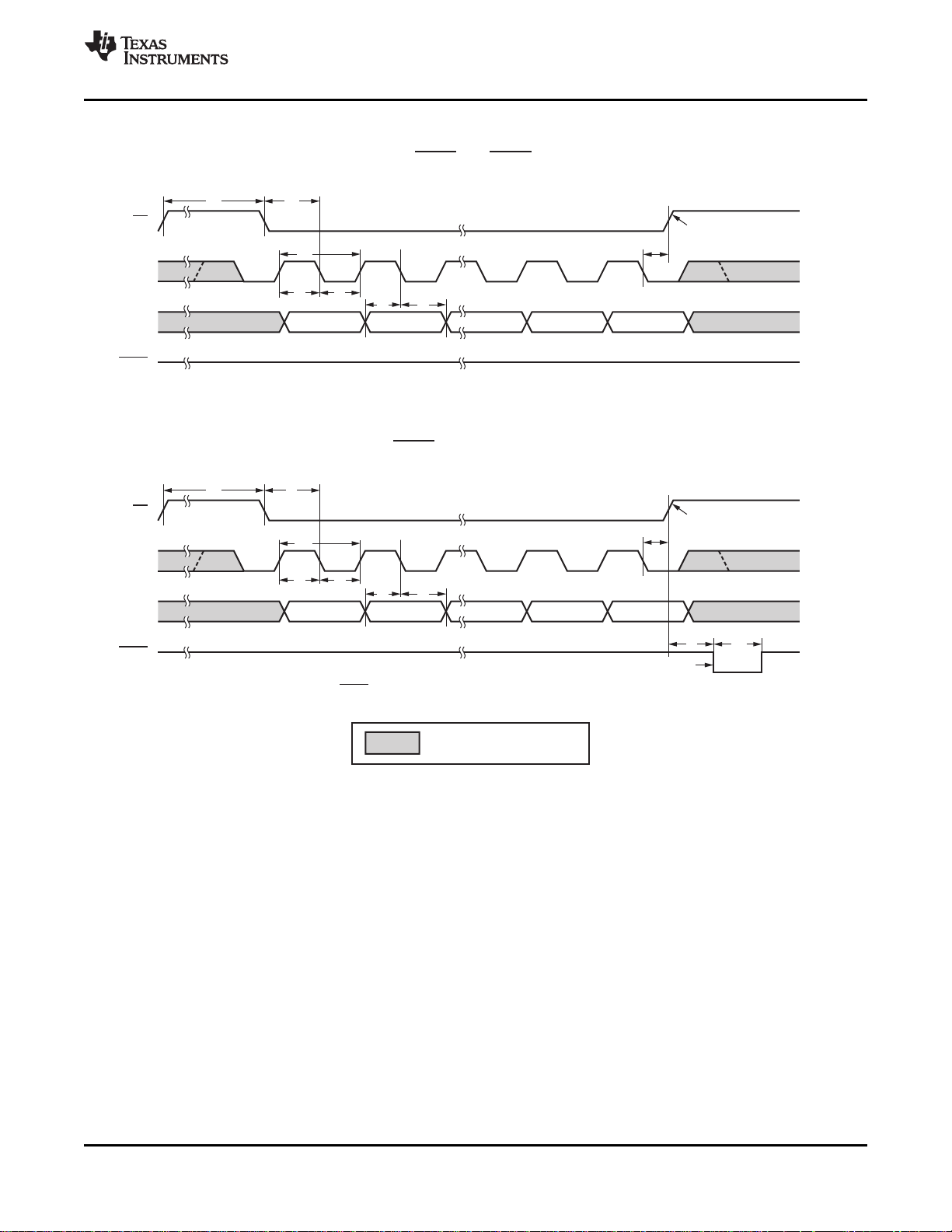
t
8
CS
SCLK
InputDataRegisterand
DACLatchUpdated
WhenCorrectionCompletes
(1)
DACLatchUpdated
(2)
SDI
BIT23(MSB)
BIT23(MSB)
BIT22 BIT1
Low
BIT0
LDAC
Ifthecorrectionengineisoff,theDAClatchisreloadedimmediatelyaftertheDACDataRegisterisupdated.NOTE:(1)
TheDAClatchisupdatedwhen goeslow,aslongasthetimingrequirementoft issatisfied.
9
LDAC
NOTE:(2)
t
4
t
1
t
2
t
5
t
6
t
7
Case1:Standalonemode:Updatewithout pin; tiedtologiclowLDAC LDAC pin .
t
8
CS
SCLK
InputDataRegisterUpdated,
butDACLatchisNot Updated
SDI
BIT22 BIT1
High
BIT0
LDAC
t
4
t
1
t
2
t
5
t
6
t
7
t
9
Case2:Standalonemode:Updatewith pin.LDAC
t
10
=Don’tCare
Bit23=MSB
Bit0=LSB
t
3
t
3
DAC7718
www.ti.com
TIMING DIAGRAMS
SBAS361A –MAY 2009–REVISED DECEMBER 2009
Figure 2. SPI Timing for Standalone Mode
Copyright © 2009, Texas Instruments Incorporated Submit Documentation Feedback 13
Product Folder Link(s): DAC7718
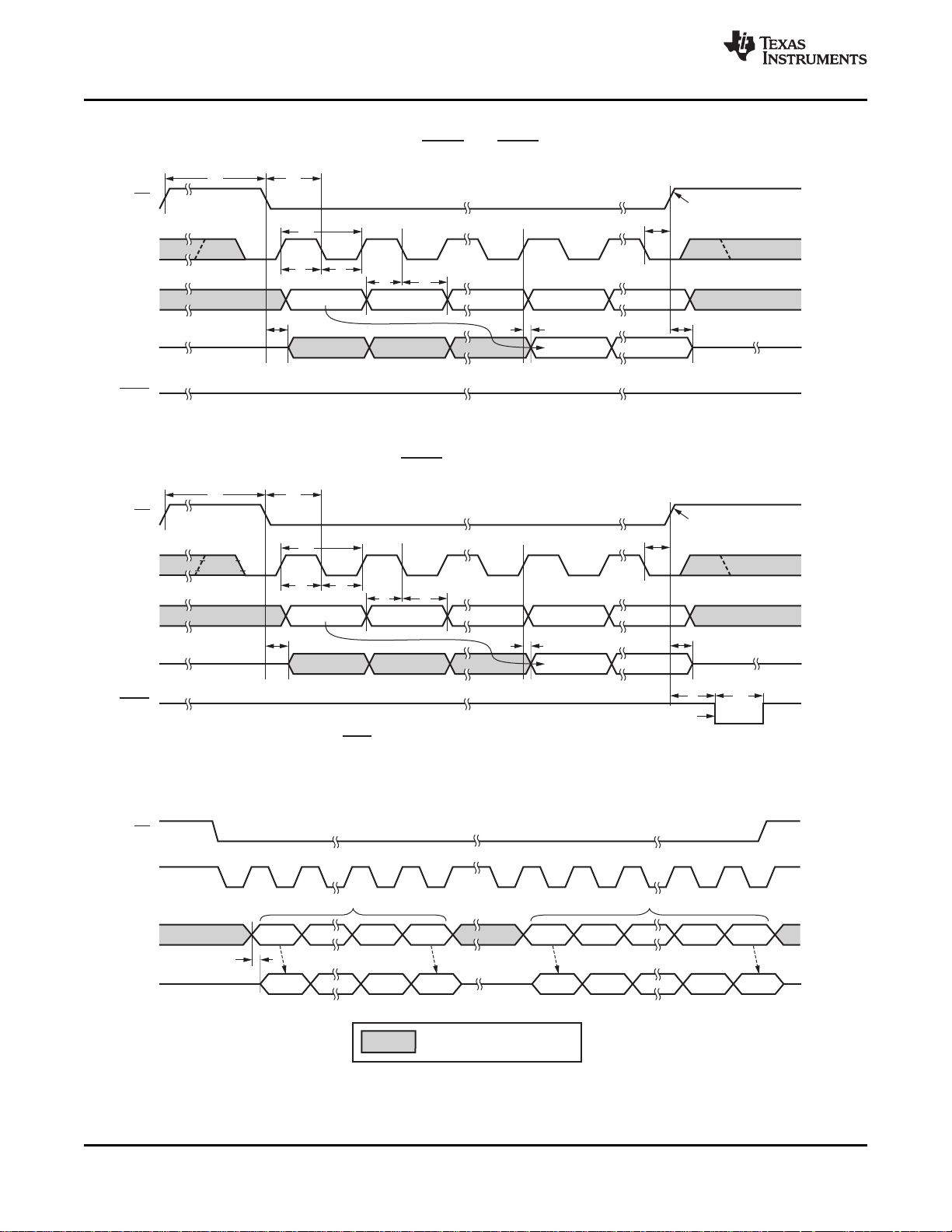
t
8
CS
SCLK
SDI
BIT23(N)
BIT22(N) BIT0(N) BIT23(N+1)
BIT23(N) BIT0(N)
Low
BIT0(N+1)
SDO
LDAC
Ifthecorrectionengineisoff,theDAClatchisreloadedimmediatelyaftertheDACDataRegisterisupdated.NOTE:(1)
TheDAClatchisupdatedwhen goeslow.Theproperdataareloadedifthet timingrequirementissatisfied.
Otherwise,invaliddataareloaded.
9
LDAC
NOTE:(2)
t
4
t
1
t
2
t
5
t
6
t
7
Case3:Daisy-ChainMode:Updatewithout pin; pintiedtologiclow.LDAC LDAC
High
LDAC
t
9
t
10
=Don’tCare
Bit23=MSB
Bit0=LSB
t
11
t
8
CS
SCLK
InputDataRegisterUpdated,
butDACLatchisNotUpdated
SDI
BIT23(N)
BIT22(N) BIT0(N) BIT23(N+1)
BIT23(N) BIT0(N)
BIT0(N+1)
SDO
t
4
t
1
t
2
t
5
t
6
t
7
Case4:Daisy-ChainMode:Updatewith pin.LDAC
t
11
t
14
DACLatchUpdated
(2)
InputDataRegisterand
DACLatchUpdated
WhenCorrectionCompletes
(1)
DB23 DB0
Case5:Daisy-ChainMode:Sleeping.
CS
SCLK
SDI
FirstWord LastWord
DB23 DB0
DB23 DB0
SDO
DB23 DB0
t
12
t
12
Hi-Z
Hi-Z Hi-Z Hi-Z
Hi-Z Hi-Z
t
13
t
13
t
3
t
3
Hi-Z
DAC7718
SBAS361A –MAY 2009–REVISED DECEMBER 2009
TIMING DIAGRAMS (continued)
www.ti.com
Figure 3. SPI Timing for Daisy-Chain Mode
14 Submit Documentation Feedback Copyright © 2009, Texas Instruments Incorporated
Product Folder Link(s): DAC7718
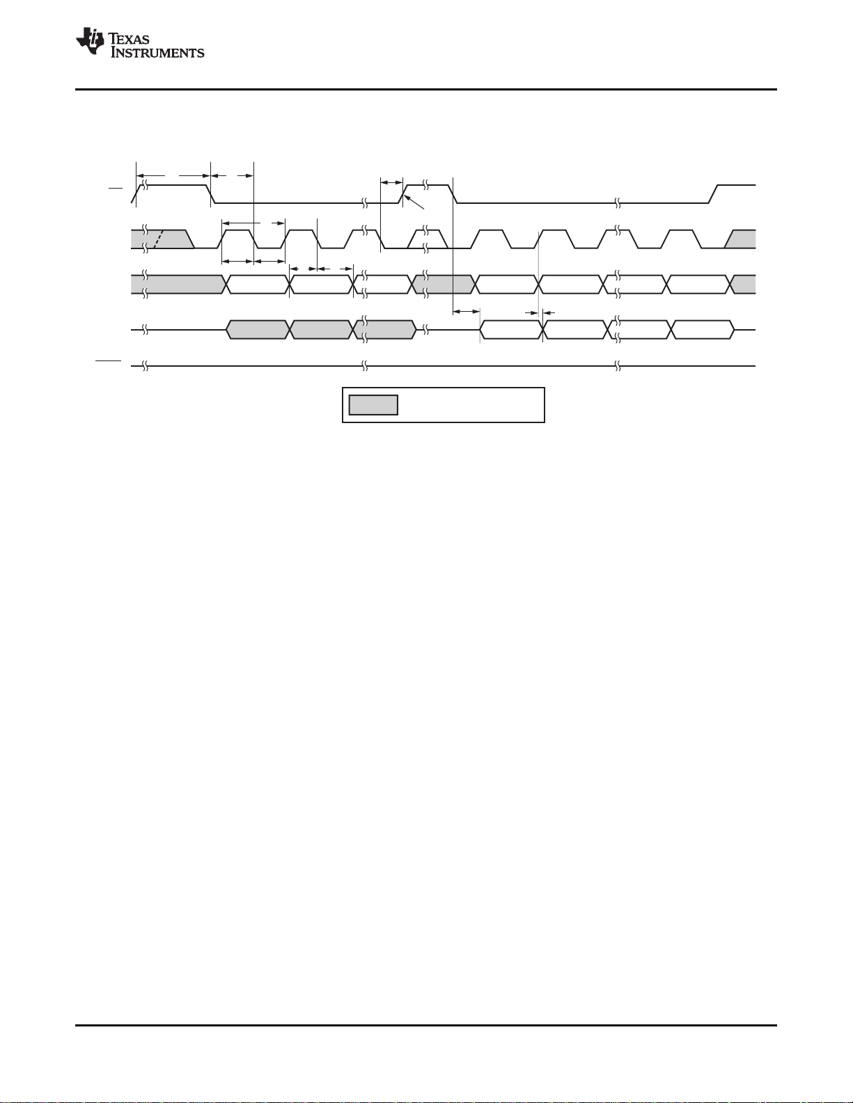
Case6:ReadbackforStandalonemode.
t
8
t
4
t
1
t
2
t
7
t
6
BIT23(=1) BIT22
InputWordSpecifiesRegistertobeRead
NOPCommand(write ‘1’ toNOPbit)
DatafromtheSelectedRegister
BIT0
BIT23
BIT23(=1)
BIT22
BIT22
BIT1
BIT1
BIT0
BIT0
InternalRegisterUpdated
CS
SCLK
SDI
SDO
LDAC
Low
t
13
t
11
=Don’tCare
Bit23=MSB
Bit0=LSB
Hi-Z Hi-Z Hi-Z
t
3
t
5
DAC7718
www.ti.com
TIMING DIAGRAMS (continued)
Figure 4. SPI Timing for Readback Operation in Standalone Mode
SBAS361A –MAY 2009–REVISED DECEMBER 2009
Copyright © 2009, Texas Instruments Incorporated Submit Documentation Feedback 15
Product Folder Link(s): DAC7718
DAC7718
SBAS361A –MAY 2009–REVISED DECEMBER 2009
TIMING CHARACTERISTICS: IOVDD= +5V
(1)(2)(3)(4)
At –40°C to +105°C, DVDD= +5V, and IOVDD= +5V, unless otherwise noted.
PARAMETER MIN MAX UNIT
f
SCLK
t
1
t
2
t
3
t
4
t
5
t
6
t
7
t
8
t
9
t
10
t
11
t
12
t
13
t
14
Clock frequency 50 MHz
SCLK cycle time 20 ns
SCLK high time 10 ns
SCLK low time 7 ns
CS falling edge to SCLK falling edge setup time 8 ns
SDI setup time before falling edge of SCLK 5 ns
SDI hold time after falling edge of SCLK 5 ns
SCLK falling edge to CS rising edge 5 ns
CS high time 10 ns
CS rising edge to LDAC falling edge 5 ns
LDAC pulse duration 10 ns
Delay from SCLK rising edge to SDO valid 3 8 ns
Delay from CS rising edge to SDO Hi-Z 5 ns
Delay from CS falling edge to SDO valid 6 ns
SDI to SDO delay during sleep mode 2 5 ns
(1) Specified by design. Not production tested.
(2) Sample tested during the initial release and after any redesign or process changes that may affect these parameters.
(3) All input signals are specified with tR= tF= 2ns (10% to 90% of IOVDD) and timed from a voltage level of IOVDD/2.
(4) SDO loaded with 10Ω series resistance and 10pF load capacitance for SDO timing specifications.
BLANKSPACE
www.ti.com
TIMING CHARACTERISTICS: IOVDD= +3V
(1)(2)(3)(4)
At –40°C to +105°C, DVDD= +3V/+5V, and IOVDD= +3V, unless otherwise noted.
PARAMETER MIN MAX UNIT
f
SCLK
t
1
t
2
t
3
t
4
t
5
t
6
t
7
t
8
t
9
t
10
t
11
t
12
t
13
t
14
(1) Specified by design. Not production tested.
(2) Sample tested during the initial release and after any redesign or process changes that may affect these parameters.
(3) All input signals are specified with tR= tF= 3ns (10% to 90% of IOVDD) and timed from a voltage level of IOVDD/2.
(4) SDO loaded with 10Ω series resistance and 10pF load capacitance for SDO timing specifications.
Clock frequency 25 MHz
SCLK cycle time 40 ns
SCLK high time 19 ns
SCLK low time 7 ns
CS falling edge to SCLK falling edge setup time 15 ns
SDI setup time before falling edge of SCLK 5 ns
SDI hold time after falling edge of SCLK 5 ns
SCLK falling edge to CS rising edge 10 ns
CS high time 19 ns
CS rising edge to LDAC falling edge 5 ns
LDAC pulse duration 10 ns
Delay from SCLK rising edge to SDO valid 3 15 ns
Delay from CS rising edge to SDO Hi-Z 7 ns
Delay from CS falling edge to SDO valid 10 ns
SDI to SDO delay during sleep mode 2 10 ns
16 Submit Documentation Feedback Copyright © 2009, Texas Instruments Incorporated
Product Folder Link(s): DAC7718
DAC7718
www.ti.com
TIMING CHARACTERISTICS: IOVDD= +1.8V
(1)(2)(3)(4)
SBAS361A –MAY 2009–REVISED DECEMBER 2009
At –40°C to +105°C, DVDD= +3V/+5V, and IOVDD= +1.8V, unless otherwise noted.
PARAMETER MIN MAX UNIT
f
SCLK
t
1
t
2
t
3
t
4
t
5
t
6
t
7
t
8
t
9
t
10
t
11
t
12
t
13
t
14
(1) Specified by design. Not production tested.
(2) Sample tested during the initial release and after any redesign or process changes that may affect these parameters.
(3) All input signals are specified with tR= tF= 6ns (10% to 90% of IOVDD) and timed from a voltage level of IOVDD/2.
(4) SDO loaded with 10Ω series resistance and 10pF load capacitance for SDO timing specifications.
Clock frequency 16.6 MHz
SCLK cycle time 60 ns
SCLK high time 28 ns
SCLK low time 7 ns
CS falling edge to SCLK falling edge setup time 28 ns
SDI setup time before falling edge of SCLK 10 ns
SDI hold time after falling edge of SCLK 5 ns
SCLK falling edge to CS rising edge 10 ns
CS high time 28 ns
CS rising edge to LDAC falling edge 5 ns
LDAC pulse duration 10 ns
Delay from SCLK rising edge to SDO valid 3 25 ns
Delay from CS rising edge to SDO Hi-Z 15 ns
Delay from CS falling edge to SDO valid 23 ns
SDI to SDO delay during sleep mode 2 25 ns
Copyright © 2009, Texas Instruments Incorporated Submit Documentation Feedback 17
Product Folder Link(s): DAC7718
1.0
0.8
0.6
0.4
0.2
0
-0.2
-0.4
-0.6
-0.8
-1.0
INLError(LSB)
AllEightChannelsShown
512
0
4096358430722560204815361024
DigitalInputCode
1.0
0.8
0.6
0.4
0.2
0
-0.2
-0.4
-0.6
-0.8
-1.0
DNLError(LSB)
AllEightChannelsShown
512
0
4096358430722560204815361024
DigitalInputCode
1.0
0.8
0.6
0.4
0.2
0
-0.2
-0.4
-0.6
-0.8
-1.0
INLError(LSB)
512
0
4096358430722560204815361024
DigitalInputCode
TypicalChannelShown
Gain=4
1.0
0.8
0.6
0.4
0.2
0
-0.2
-0.4
-0.6
-0.8
-1.0
DNLError(LSB)
512
0
4096358430722560204815361024
DigitalInputCode
TypicalChannelShown
Gain=4
DAC7718
SBAS361A –MAY 2009–REVISED DECEMBER 2009
TYPICAL CHARACTERISTICS: Bipolar
At TA= 25°C, AVDD= 16.5V, AVSS= –16.5V, V
LINEARITY ERROR DIFFERENTIAL LINEARITY ERROR
vs DIGITAL INPUT CODE (All 8 Channels) vs DIGITAL INPUT CODE (All 8 Channels)
Figure 5. Figure 6.
LINEARITY ERROR DIFFERENTIAL LINEARITY ERROR
vs DIGITAL INPUT CODE (+25°C) vs DIGITAL INPUT CODE (+25°C)
www.ti.com
= IOVDD= DVDD= 5V, gain = 6, data format=USB, unless otherwise noted.
REF
Figure 7. Figure 8.
18 Submit Documentation Feedback Copyright © 2009, Texas Instruments Incorporated
Product Folder Link(s): DAC7718
1.0
0.8
0.6
0.4
0.2
0
-0.2
-0.4
-0.6
-0.8
-1.0
INLError(LSB)
512
0
4096358430722560204815361024
DigitalInputCode
TypicalChannelShown
1.0
0.8
0.6
0.4
0.2
0
-0.2
-0.4
-0.6
-0.8
-1.0
DNLError(LSB)
512
0
4096358430722560204815361024
DigitalInputCode
TypicalChannelShown
1.0
0.8
0.6
0.4
0.2
0
-0.2
-0.4
-0.6
-0.8
-1.0
INLError(LSB)
512
0
4096358430722560204815361024
DigitalInputCode
TypicalChannelShown
1.0
0.8
0.6
0.4
0.2
0
-0.2
-0.4
-0.6
-0.8
-1.0
DNLError(LSB)
512
0
4096358430722560204815361024
DigitalInputCode
TypicalChannelShown
1.0
0.8
0.6
0.4
0.2
0
-0.2
-0.4
-0.6
-0.8
-1.0
INLError(LSB)
512
0
4096358430722560204815361024
DigitalInputCode
TypicalChannelShown
1.0
0.8
0.6
0.4
0.2
0
-0.2
-0.4
-0.6
-0.8
-1.0
DNLError(LSB)
512
0
4096358430722560204815361024
DigitalInputCode
TypicalChannelShown
DAC7718
www.ti.com
TYPICAL CHARACTERISTICS: Bipolar (continued)
At TA= 25°C, AVDD= 16.5V, AVSS= –16.5V, V
LINEARITY ERROR DIFFERENTIAL LINEARITY ERROR
vs DIGITAL INPUT CODE (–40°C) vs DIGITAL INPUT CODE (–40°C)
Figure 9. Figure 10.
LINEARITY ERROR DIFFERENTIAL LINEARITY ERROR
vs DIGITAL INPUT CODE (+25°C) vs DIGITAL INPUT CODE (+25°C)
SBAS361A –MAY 2009–REVISED DECEMBER 2009
= IOVDD= DVDD= 5V, gain = 6, data format=USB, unless otherwise noted.
REF
Figure 11. Figure 12.
LINEARITY ERROR DIFFERENTIAL LINEARITY ERROR
vs DIGITAL INPUT CODE (+105°C) vs DIGITAL INPUT CODE (+105°C)
Figure 13. Figure 14.
Copyright © 2009, Texas Instruments Incorporated Submit Documentation Feedback 19
Product Folder Link(s): DAC7718

INLError(LSB)
-55 -40 -25 -10 5 20 35 50 65 80 95 110 125
Temperature(°C)
1.0
0.8
0.6
0.4
0.2
0
0.2
0.4
0.6
0.8
1.0
-
-
-
-
-
INLMax
INLMin
DNLError(LSB)
-55 -40 -25 -10 5 20 35 50 65 80 95 110 125
Temperature(°C)
1.0
0.8
0.6
0.4
0.2
0
0.2
0.4
0.6
0.8
1.0
-
-
-
-
-
DNLMax
DNLMin
INLError(LSB)
-55 -40 -25 -10 5 20 35 50 65 80 95 110 125
Temperature(°C)
1.0
0.8
0.6
0.4
0.2
0
0.2
0.4
0.6
0.8
1.0
-
-
-
-
-
Gain=4
INLMax
INLMin
DNLError(LSB)
-55 -40 -25 -10 5 20 35 50 65 80 95 110 125
Temperature(°C)
1.0
0.8
0.6
0.4
0.2
0
0.2
0.4
0.6
0.8
1.0
-
-
-
-
-
Gain=4
DNLMax
DNLMin
1.0
0.8
0.6
0.4
0.2
0
0.2
0.4
0.6
0.8
1.0
-
-
-
-
-
INLError(LSB)
1.0 1.5 2.0 2.5 3.0 3.5 4.0 4.5 5.0 5.5
V (V)
REF
INLMin
AVDD=+18V
AVSS= 18V-
INLMax
1.0
0.8
0.6
0.4
0.2
0
0.2
0.4
0.6
0.8
1.0
-
-
-
-
-
DNLError(LSB)
1.0 1.5 2.0 2.5 3.0 3.5 4.0 4.5 5.0 5.5
V (V)
REF
DNLMax
DNLMin
AVDD=+18V
AVSS= 18V-
DAC7718
SBAS361A –MAY 2009–REVISED DECEMBER 2009
TYPICAL CHARACTERISTICS: Bipolar (continued)
At TA= 25°C, AVDD= 16.5V, AVSS= –16.5V, V
LINEARITY ERROR DIFFERENTIAL LINEARITY ERROR
vs TEMPERATURE vs TEMPERATURE
Figure 15. Figure 16.
LINEARITY ERROR DIFFERENTIAL LINEARITY ERROR
vs TEMPERATURE vs TEMPERATURE
www.ti.com
= IOVDD= DVDD= 5V, gain = 6, data format=USB, unless otherwise noted.
REF
Figure 17. Figure 18.
LINEARITY ERROR DIFFERENTIAL LINEARITY ERROR
vs REFERENCE VOLTAGE vs REFERENCE VOLTAGE
20 Submit Documentation Feedback Copyright © 2009, Texas Instruments Incorporated
Figure 19. Figure 20.
Product Folder Link(s): DAC7718

1.0
0.8
0.6
0.4
0.2
0
-0.2
-0.4
-0.6
-0.8
-1.0
INLError(LSB)
4.5 6.0 7.5 9.0 10.5 12.0 13.5 15.0 16.5 18.0
AV =
DD S S
-AV (V)
INLMax
DV
DD DD
=IOV =4.5V
V =2.048V
REF
Gain=4
INLMin
1.0
0.8
0.6
0.4
0.2
0
-0.2
-0.4
-0.6
-0.8
-1.0
DNLError(LSB)
4.5 6.0 7.5 9.0 10.5 12.0 13.5 15.0 16.5 18.0
AV =
DD S S
-AV (V)
DNLMax
DV
DD DD
=IOV =4.5V
V =2.048V
REF
Gain=4
DNLMin
5
4
3
2
1
0
-1
-2
-3
-4
-5
BipolarZeroError(mV)
4.5 6.0 7.5 9.0 10.5 12.0 13.5 15.0 16.5 18.0
AV = AV (V)
DD S S
-
DVDD=IOV
DD
REF
=4.5V
V =2.048V
Gain=4
Ch0
Ch1
Ch2
Ch3
Ch4
Ch5
Ch6
Ch7
5
4
3
2
1
0
-1
-2
-3
-4
-5
BipolarGainError(mV)
4.5 6.0 7.5 9.0 10.5 12.0 13.5 15.0 16.5 18.0
AV = AV (V)
DD S S
-
DVDD=IOV
DD
REF
=4.5V
V =2.048V
Gain=4
Ch0
Ch1
Ch2
Ch3
Ch4
Ch5
Ch6
Ch7
5
4
3
2
1
0
-1
-2
-3
-4
-5
BipolarZeroError(mV)
1.0
1.5 2.0 2.5 3.0 3.5 4.0 4.5 5.0 5.5
V (V)
REF
Ch0
Ch1
Ch2
Ch3
Ch4
Ch5
Ch6
Ch7
AV =+18V
AV = 18V
DD
SS
-
5
4
3
2
1
0
-1
-2
-3
-4
-5
BipolarZeroError(mV)
1.0
1.5 2.0 2.5 3.0 3.5 4.0 4.5 5.0 5.5
V (V)
REF
Ch0
Ch1
Ch2
Ch3
Ch4
Ch5
Ch6
Ch7
AV =+18V
AV = 18V
Gain=4
DD
SS
-
DAC7718
www.ti.com
TYPICAL CHARACTERISTICS: Bipolar (continued)
At TA= 25°C, AVDD= 16.5V, AVSS= –16.5V, V
LINEARITY ERROR DIFFERENTIAL LINEARITY ERROR
vs AVDDAND AV
Figure 21. Figure 22.
BIPOLAR ZERO ERROR BIPOLAR GAIN ERROR
vs AVDDAND AV
SS
SS
SBAS361A –MAY 2009–REVISED DECEMBER 2009
= IOVDD= DVDD= 5V, gain = 6, data format=USB, unless otherwise noted.
REF
vs AVDDAND AV
vs AVDDAND AV
SS
SS
Figure 23. Figure 24.
BIPOLAR ZERO ERROR BIPOLAR ZERO ERROR
vs REFERENCE VOLTAGE vs REFERENCE VOLTAGE
Copyright © 2009, Texas Instruments Incorporated Submit Documentation Feedback 21
Figure 25. Figure 26.
Product Folder Link(s): DAC7718

5
4
3
2
1
0
-1
-2
-3
-4
-5
BipolarGainError(mV)
1.0
1.5 2.0 2.5 3.0 3.5 4.0 4.5 5.0 5.5
V (V)
REF
AV =+18V
AV = 18V
DD
SS
-
Ch0
Ch1
Ch2
Ch3
Ch4
Ch5
Ch6
Ch7
5
4
3
2
1
0
-1
-2
-3
-4
-5
BipolarGainError(mV)
1.0
1.5 2.0 2.5 3.0 3.5 4.0 4.5 5.0 5.5
V (V)
REF
Ch0
Ch1
Ch2
Ch3
Ch4
Ch5
Ch6
Ch7
AV =+18V
AV = 18V
Gain=4
DD
SS
-
BipolarZeroError(mV)
-55 -40 -25 -10 5 20 35 50 65 80 95 110 125
Temperature(°C)
5
4
3
2
1
0
1
2
3
4
5
-
-
-
-
-
Ch0
Ch1
Ch2
Ch3
Ch4
Ch5
Ch6
Ch7
BipolarZeroError(mV)
-55 -40 -25 -10 5 20 35 50 65 80 95 110 125
Temperature(°C)
5
4
3
2
1
0
1
2
3
4
5
-
-
-
-
-
Gain=4
Ch0
Ch1
Ch2
Ch3
Ch4
Ch5
Ch6
Ch7
BipolarGainError(mV)
-55 -40 -25 -10 5 20 35 50 65 80 95 110 125
Temperature(°C)
5
4
3
2
1
0
1
2
3
4
5
-
-
-
-
-
Ch0
Ch1
Ch2
Ch3
Ch4
Ch5
Ch6
Ch7
BipolarGainError(mV)
-55 -40 -25 -10 5 20 35 50 65 80 95 110 125
Temperature(°C)
5
4
3
2
1
0
1
2
3
4
5
-
-
-
-
-
Gain=4
Ch0
Ch1
Ch2
Ch3
Ch4
Ch5
Ch6
Ch7
DAC7718
SBAS361A –MAY 2009–REVISED DECEMBER 2009
TYPICAL CHARACTERISTICS: Bipolar (continued)
At TA= 25°C, AVDD= 16.5V, AVSS= –16.5V, V
BIPOLAR GAIN ERROR BIPOLAR GAIN ERROR
vs REFERENCE VOLTAGE vs REFERENCE VOLTAGE
Figure 27. Figure 28.
BIPOLAR ZERO ERROR BIPOLAR ZERO ERROR
vs TEMPERATURE vs TEMPERATURE
www.ti.com
= IOVDD= DVDD= 5V, gain = 6, data format=USB, unless otherwise noted.
REF
Figure 29. Figure 30.
BIPOLAR GAIN ERROR BIPOLAR GAIN ERROR
vs TEMPERATURE vs TEMPERATURE
22 Submit Documentation Feedback Copyright © 2009, Texas Instruments Incorporated
Figure 31. Figure 32.
Product Folder Link(s): DAC7718

8
7
6
5
4
3
2
1
0
AnalogPower-SupplyCurrent(mA)
-55 -40 -25 -10 5 20 35 50 65 80 95 110 125
Temperature(°C)
I
AVDD
-I
AVSS
8
7
6
5
4
3
2
1
0
AnalogPower-SupplyCurrent(mA)
-I
AVSS
I
AVDD
1.0 5.55.04.54.03.53.01.5 2.0
V (V)
REF
2.5
AllDACsLoadedwithMidscaleCode
AVDD=+18V
A =VSS-18V
8
6
4
2
0
-2
-4
-6
-8
AnalogPower-SupplyCurrent(mA)
512
0
4096358430722560204815361024
DigitalInputCode
AllDACsLoadedwithSameCode
I
AVDD
I
AVSS
250
200
150
100
50
0
DigitalPower-SupplyCurrent( A)m
0 0.5 1.0 1.5 2.0 2.5 3.0 3.5 4.0 4.5 5.0 5.5
LogicInputVoltage(V)
SweepFrom
5.5Vto0V
SweepFrom
0Vto5.5V
OneDigitalInputSwept,AllOthersatGNDorIOV
DD
DV (mV)
OUT
-15 -9 -3 3 9-12 -6 0 6 12 15
CurrentOutputI (mA)
OUT
6
5
4
3
2
1
0
1
2
3
4
5
-
-
-
-
--6
FFFh
C00h
800h
400h
000h
2000
1800
1600
1400
1200
1000
800
600
400
200
0
Noise(nV/ )ÖHz
1 100k10k1k10010
Frequency(Hz)
DACLoadedwithMidscaleCode
Gain=6
Gain=4
DAC7718
www.ti.com
TYPICAL CHARACTERISTICS: Bipolar (continued)
At TA= 25°C, AVDD= 16.5V, AVSS= –16.5V, V
ANALOG POWER-SUPPLY CURRENT ANALOG POWER-SUPPLY CURRENT
vs TEMPERATURE vs REFERENCE VOLTAGE
Figure 33. Figure 34.
ANALOG POWER-SUPPLY CURRENT DIGITAL POWER-SUPPLY CURRENT
vs DIGITAL INPUT CODE vs LOGIC INPUT VOLTAGE
SBAS361A –MAY 2009–REVISED DECEMBER 2009
= IOVDD= DVDD= 5V, gain = 6, data format=USB, unless otherwise noted.
REF
Figure 35. Figure 36.
DELTA OUTPUT VOLTAGE DAC OUTPUT NOISE DENSITY
vs SOURCE AND SINK CURRENTS vs FREQUENCY
Copyright © 2009, Texas Instruments Incorporated Submit Documentation Feedback 23
Figure 37. Figure 38.
Product Folder Link(s): DAC7718

Time(10 s/div)m
1LSB/div
5V/div
FromCode:000h
ToCode:
Load:10k ||240pF
FFFh
W
Large-SignalV
OUT
Small-SignalError
TriggerPulse: LDAC
5V/div
Time(10 s/div)m
1LSB/div
5V/div
FromCode:FFFh
ToCode:
Load:10k ||240pF
000h
W
Large-SignalV
OUT
Small-SignalError
TriggerPulse: LDAC
5V/div
Time(10 s/div)m
1LSB/div
5V/div
FromCode:400h
ToCode:
Load:10k ||240pF
C00h
W
Large-SignalV
OUT
Small-SignalError
TriggerPulse: LDAC
5V/div
Time(10 s/div)m
1LSB/div
5V/div
FromCode:C00h
ToCode:
Load:10k ||240pF
400h
W
Large-SignalV
OUT
Small-SignalError
TriggerPulse: LDAC
5V/div
Time(2 s/div)m
V (3mV/div)
OUT
GlitchImpulse
TriggerPulse5V/div
FromCode:7FFh
ToCode: 800h
Channel0asExample
Load:10k ||200pFW
Time(2 s/div)m
V (3mV/div)
OUT
GlitchImpulse
TriggerPulse5V/div
FromCode:800h
ToCode: 7FFh
Channel0asExample
Load:10k ||200pFW
DAC7718
SBAS361A –MAY 2009–REVISED DECEMBER 2009
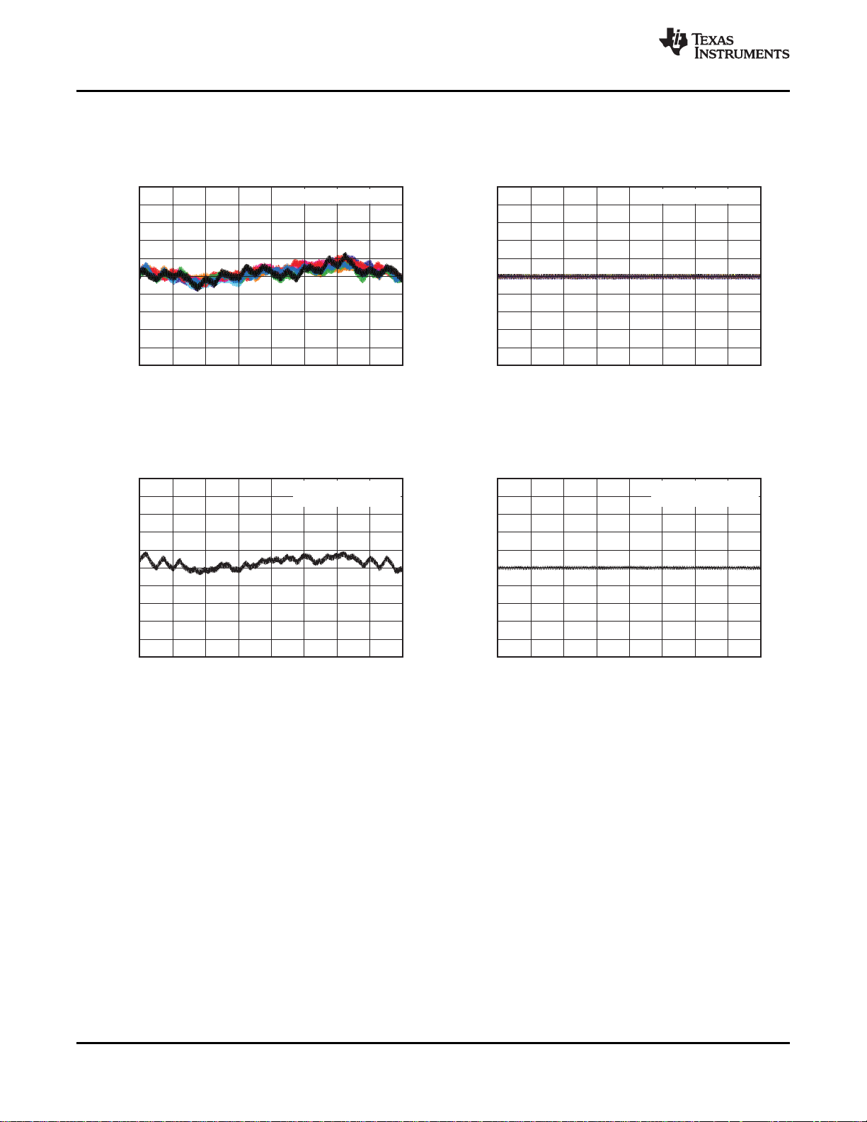
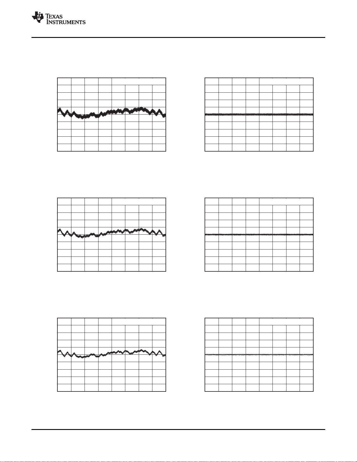
TYPICAL CHARACTERISTICS: Bipolar (continued)
At TA= 25°C, AVDD= 16.5V, AVSS= –16.5V, V
SETTLING TIME SETTLING TIME
–15V TO +15V TRANSITION +15V TO –15V TRANSITION
Figure 39. Figure 40.
SETTLING TIME SETTLING TIME
1/4 TO 3/4 FULL-SCALE TRANSITION 3/4 TO 1/4 FULL-SCALE TRANSITION
www.ti.com
= IOVDD= DVDD= 5V, gain = 6, data format=USB, unless otherwise noted.
REF
Figure 41. Figure 42.
GLITCH ENERGY GLITCH ENERGY
1 LSB STEP, RISING EDGE 1 LSB STEP, FALLING EDGE
24 Submit Documentation Feedback Copyright © 2009, Texas Instruments Incorporated
Figure 43. Figure 44.
Product Folder Link(s): DAC7718

60
55
50
45
40
35
30
25
20
15
10
5
0
Population(%)
1.0
0.8
0.6
0.4
0.2
0
0.2
0.4
0.6
0.8
1.0
-
-
-
-
-
BipolarZeroError(LSB)
60
55
50
45
40
35
30
25
20
15
10
5
0
Population(%)
Gain=4
1.0
0.8
0.6
0.4
0.2
0
0.2
0.4
0.6
0.8
1.0
-
-
-
-
-
BipolarZeroError(LSB)
40
35
30
25
20
15
10
5
0
Population(%)
-1.0
0.8
0.6
0.4
0.2
0
0.2
0.4
0.6
0.8
1.0
-
-
-
-
BipolarGainError(LSB)
Gain=4
40
35
30
25
20
15
10
5
0
Population(%)
-1.0
0.8
0.6
0.4
0.2
0
0.2
0.4
0.6
0.8
1.0
-
-
-
-
BipolarGainError(LSB)
45
40
35
30
25
20
15
10
5
0
Population(%)
2.8
3.0
3.2
3.4
3.6
3.8
4.0
4.2
4.4
4.6
4.8
5.0
5.2
5.4
5.6
5.8
6.0
AI (mA)
DD
55
50
45
40
35
30
25
20
15
10
5
0
Population(%)
-4.0
3.8
3.6
3.4
3.2
3.0
2.8
2.6
2.4
2.2
2.0
1.8
1.6
1.4
1.2
1.0
-
-
-
-
-
-
-
-
-
-
-
-
-
-
-
AI (mA)
SS
DAC7718
www.ti.com
TYPICAL CHARACTERISTICS: Bipolar (continued)
At TA= 25°C, AVDD= 16.5V, AVSS= –16.5V, V
BIPOLAR ZERO ERROR BIPOLAR ZERO ERROR
HISTOGRAM HISTOGRAM
Figure 45. Figure 46.
BIPOLAR GAIN ERROR BIPOLAR GAIN ERROR
HISTOGRAM HISTOGRAM
SBAS361A –MAY 2009–REVISED DECEMBER 2009
= IOVDD= DVDD= 5V, gain = 6, data format=USB, unless otherwise noted.
REF
Figure 47. Figure 48.
NEGATIVE ANALOG POWER SUPPLY POSITIVE ANALOG POWER SUPPLY
HISTOGRAM HISTOGRAM
Figure 49. Figure 50.
Copyright © 2009, Texas Instruments Incorporated Submit Documentation Feedback 25
Product Folder Link(s): DAC7718

Time(2 s/div)m
DACCode=800h
NoLoad
Gain=6
Channel0asExample
V (5 V/div)m
OUT
Time(2 s/div)m
DACCode=800h
NoLoad
Gain=4
Channel0asExample
V (5 V/div)m
OUT
DAC7718
SBAS361A –MAY 2009–REVISED DECEMBER 2009
TYPICAL CHARACTERISTICS: Bipolar (continued)
At TA= 25°C, AVDD= 16.5V, AVSS= –16.5V, V
DAC OUTPUT NOISE DAC OUTPUT NOISE
0.1Hz TO 10Hz 0.1Hz TO 10Hz
Figure 51. Figure 52.
www.ti.com
= IOVDD= DVDD= 5V, gain = 6, data format=USB, unless otherwise noted.
REF
26 Submit Documentation Feedback Copyright © 2009, Texas Instruments Incorporated
Product Folder Link(s): DAC7718

1.0
0.8
0.6
0.4
0.2
0
-0.2
-0.4
-0.6
-0.8
-1.0
INLError(LSB)
AllEightChannelsShown
512
0
4096358430722560204815361024
DigitalInputCode
1.0
0.8
0.6
0.4
0.2
0
-0.2
-0.4
-0.6
-0.8
-1.0
DNLError(LSB)
AllEightChannelsShown
512
0
4096358430722560204815361024
DigitalInputCode
1.0
0.8
0.6
0.4
0.2
0
-0.2
-0.4
-0.6
-0.8
-1.0
INLError(LSB)
512
0
4096358430722560204815361024
DigitalInputCode
TypicalChannelShown
Gain=4
1.0
0.8
0.6
0.4
0.2
0
-0.2
-0.4
-0.6
-0.8
-1.0
DNLError(LSB)
512
0
4096358430722560204815361024
DigitalInputCode
TypicalChannelShown
Gain=4
DAC7718
www.ti.com
At TA= 25°C, AVDD= 32V, AVSS= 0V, V
LINEARITY ERROR DIFFERENTIAL LINEARITY ERROR
vs DIGITAL INPUT CODE (All 8 Channels) vs DIGITAL INPUT CODE (All 8 Channels)
Figure 53. Figure 54.
LINEARITY ERROR DIFFERENTIAL LINEARITY ERROR
vs DIGITAL INPUT CODE (+25°C) vs DIGITAL INPUT CODE (+25°C)
SBAS361A –MAY 2009–REVISED DECEMBER 2009
TYPICAL CHARACTERISTICS: Unipolar
= 5V, IOVDD= DVDD= 5V, gain = 6, data format=USB, unless otherwise noted.
REF
Figure 55. Figure 56.
Copyright © 2009, Texas Instruments Incorporated Submit Documentation Feedback 27
Product Folder Link(s): DAC7718

1.0
0.8
0.6
0.4
0.2
0
-0.2
-0.4
-0.6
-0.8
-1.0
INLError(LSB)
512
0
4096358430722560204815361024
DigitalInputCode
TypicalChannelShown
1.0
0.8
0.6
0.4
0.2
0
-0.2
-0.4
-0.6
-0.8
-1.0
DNLError(LSB)
512
0
4096358430722560204815361024
DigitalInputCode
TypicalChannelShown
1.0
0.8
0.6
0.4
0.2
0
-0.2
-0.4
-0.6
-0.8
-1.0
INLError(LSB)
512
0
4096358430722560204815361024
DigitalInputCode
TypicalChannelShown
1.0
0.8
0.6
0.4
0.2
0
-0.2
-0.4
-0.6
-0.8
-1.0
DNLError(LSB)
512
0
4096358430722560204815361024
DigitalInputCode
TypicalChannelShown
1.0
0.8
0.6
0.4
0.2
0
-0.2
-0.4
-0.6
-0.8
-1.0
INLError(LSB)
512
0
4096358430722560204815361024
DigitalInputCode
TypicalChannelShown
1.0
0.8
0.6
0.4
0.2
0
-0.2
-0.4
-0.6
-0.8
-1.0
DNLError(LSB)
512
0
4096358430722560204815361024
DigitalInputCode
TypicalChannelShown
DAC7718
SBAS361A –MAY 2009–REVISED DECEMBER 2009
TYPICAL CHARACTERISTICS: Unipolar (continued)
At TA= 25°C, AVDD= 32V, AVSS= 0V, V
LINEARITY ERROR DIFFERENTIAL LINEARITY ERROR
vs DIGITAL INPUT CODE (–40°C) vs DIGITAL INPUT CODE (–40°C)
Figure 57. Figure 58.
LINEARITY ERROR DIFFERENTIAL LINEARITY ERROR
vs DIGITAL INPUT CODE (+25°C) vs DIGITAL INPUT CODE (+25°C)
= 5V, IOVDD= DVDD= 5V, gain = 6, data format=USB, unless otherwise noted.
REF
www.ti.com
Figure 59. Figure 60.
LINEARITY ERROR DIFFERENTIAL LINEARITY ERROR
vs DIGITAL INPUT CODE (+105°C) vs DIGITAL INPUT CODE (+105°C)
Figure 61. Figure 62.
28 Submit Documentation Feedback Copyright © 2009, Texas Instruments Incorporated
Product Folder Link(s): DAC7718

INLError(LSB)
-55 -40 -25 -10 5 20 35 50 65 80 95 110 125
Temperature(°C)
1.0
0.8
0.6
0.4
0.2
0
0.2
0.4
0.6
0.8
1.0
-
-
-
-
-
Gain=4
INLMax
INLMin
DNLError(LSB)
-55 -40 -25 -10 5 20 35 50 65 80 95 110 125
Temperature(°C)
1.0
0.8
0.6
0.4
0.2
0
0.2
0.4
0.6
0.8
1.0
-
-
-
-
-
DNLMax
DNLMin
INLError(LSB)
-55 -40 -25 -10 5 20 35 50 65 80 95 110 125
Temperature(°C)
1.0
0.8
0.6
0.4
0.2
0
0.2
0.4
0.6
0.8
1.0
-
-
-
-
-
Gain=4
INLMax
INLMin
DNLError(LSB)
-55 -40 -25 -10 5 20 35 50 65 80 95 110 125
Temperature(°C)
1.0
0.8
0.6
0.4
0.2
0
0.2
0.4
0.6
0.8
1.0
-
-
-
-
-
Gain=4
DNLMax
DNLMin
1.0
0.8
0.6
0.4
0.2
0
0.2
0.4
0.6
0.8
1.0
-
-
-
-
-
INLError(LSB)
1.0 1.5 2.0 2.5 3.0 3.5 4.0 4.5 5.0 5.5
V (V)
REF
INLMin
AVDD=+36V
INLMax
1.0
0.8
0.6
0.4
0.2
0
0.2
0.4
0.6
0.8
1.0
-
-
-
-
-
DNLError(LSB)
1.0 1.5 2.0 2.5 3.0 3.5 4.0 4.5 5.0 5.5
V (V)
REF
DNLMax
DNLMin
AVDD=+36V
DAC7718
www.ti.com
TYPICAL CHARACTERISTICS: Unipolar (continued)
At TA= 25°C, AVDD= 32V, AVSS= 0V, V
LINEARITY ERROR DIFFERENTIAL LINEARITY ERROR
vs TEMPERATURE vs TEMPERATURE
Figure 63. Figure 64.
LINEARITY ERROR DIFFERENTIAL LINEARITY ERROR
vs TEMPERATURE vs TEMPERATURE
SBAS361A –MAY 2009–REVISED DECEMBER 2009
= 5V, IOVDD= DVDD= 5V, gain = 6, data format=USB, unless otherwise noted.
REF
Figure 65. Figure 66.
LINEARITY ERROR DIFFERENTIAL LINEARITY ERROR
vs REFERENCE VOLTAGE vs REFERENCE VOLTAGE
Copyright © 2009, Texas Instruments Incorporated Submit Documentation Feedback 29
Figure 67. Figure 68.
Product Folder Link(s): DAC7718

1.0
0.8
0.6
0.4
0.2
0
-0.2
-0.4
-0.6
-0.8
-1.0
INLError(LSB)
9 12
15
18 21 24 27 30 33 36
AVDD(V)
INLMax
DV
DD DD
=IOV =4.5V
V =2.048V
REF
Gain=4
INLMin
1.0
0.8
0.6
0.4
0.2
0
-0.2
-0.4
-0.6
-0.8
-1.0
DNLError(LSB)
9 12
15
18 21 24 27 30 33 36
AVDD(V)
DNLMax
DV
DD DD
=IOV =4.5V
V =2.048V
REF
Gain=4
DNLMin
5
4
3
2
1
0
-1
-2
-3
-4
-5
Zero-ScaleError(mV)
9 12 15 18 21 24 27 30 33 36
AV (V)
DD
DVDD=IOVDD=4.5V
V =2.048V
Code=010h
Gain=4
REF
Ch0
Ch1
Ch2
Ch3
Ch4
Ch5
Ch6
Ch7
5
4
3
2
1
0
-1
-2
-3
-4
-5
UnipolarGainError(mV)
9 12 15 18 21 24 27 30 33 36
AV (V)
DD
DVDD=IOVDD=4.5V
V =2.048V
REF
Gain=4
Ch0
Ch1
Ch2
Ch3
Ch4
Ch5
Ch6
Ch7
5
4
3
2
1
0
-1
-2
-3
-4
-5
Zero-ScaleError(mV)
1.0
1.5 2.0 2.5 3.0 3.5 4.0 4.5 5.0 5.5
V (V)
REF
Ch0
Ch1
Ch2
Ch3
Ch4
Ch5
Ch6
Ch7
AV =+36V
Code=010h
DD
5
4
3
2
1
0
-1
-2
-3
-4
-5
Zero-ScaleError(mV)
1.0
1.5 2.0 2.5 3.0 3.5 4.0 4.5 5.0 5.5
V (V)
REF
Ch0
Ch1
Ch2
Ch3
Ch4
Ch5
Ch6
Ch7
AV =+36V
Code=010h
Gain=4
DD
DAC7718
SBAS361A –MAY 2009–REVISED DECEMBER 2009
TYPICAL CHARACTERISTICS: Unipolar (continued)
At TA= 25°C, AVDD= 32V, AVSS= 0V, V
LINEARITY ERROR DIFFERENTIAL LINEARITY ERROR
vs ANALOG SUPPLY VOLTAGE vs ANALOG SUPPLY VOLTAGE
Figure 69. Figure 70.
ZERO-SCALE ERROR UNIPOLAR GAIN ERROR
vs ANALOG SUPPLY VOLTAGE vs ANALOG SUPPLY VOLTAGE
= 5V, IOVDD= DVDD= 5V, gain = 6, data format=USB, unless otherwise noted.
REF
www.ti.com
Figure 71. Figure 72.
ZERO-SCALE ERROR ZERO-SCALE ERROR
vs REFERENCE VOLTAGE vs REFERENCE VOLTAGE
30 Submit Documentation Feedback Copyright © 2009, Texas Instruments Incorporated
Figure 73. Figure 74.
Product Folder Link(s): DAC7718

5
4
3
2
1
0
-1
-2
-3
-4
-5
UnipolarGainError(mV)
1.0
1.5 2.0 2.5 3.0 3.5 4.0 4.5 5.0 5.5
V (V)
REF
Ch0
Ch1
Ch2
Ch3
Ch4
Ch5
Ch6
Ch7
AV =+36V
DD
5
4
3
2
1
0
-1
-2
-3
-4
-5
UnipolarGainError(mV)
1.0
1.5 2.0 2.5 3.0 3.5 4.0 4.5 5.0 5.5
V (V)
REF
Ch0
Ch1
Ch2
Ch3
Ch4
Ch5
Ch6
Ch7
AV =+36V
Gain=4
DD
Zero-ScaleError(mV)
-55 -40 -25 -10 5 20 35 50 65 80 95 110 125
Temperature(°C)
5
4
3
2
1
0
1
2
3
4
5
-
-
-
-
-
Ch0
Ch1
Ch2
Ch3
Ch4
Ch5
Ch6
Ch7
Code=010h
Zero-ScaleError(mV)
-55 -40 -25 -10 5 20 35 50 65 80 95 110 125
Temperature(°C)
5
4
3
2
1
0
1
2
3
4
5
-
-
-
-
-
Ch0
Ch1
Ch2
Ch3
Ch4
Ch5
Ch6
Ch7
Code=010h
Gain=4
UnipolarGainError(mV)
-55 -40 -25 -10 5 20 35 50 65 80 95 110 125
Temperature(°C)
5
4
3
2
1
0
1
2
3
4
5
-
-
-
-
-
Ch0
Ch1
Ch2
Ch3
Ch4
Ch5
Ch6
Ch7
UnipolarGainError(mV)
-55 -40 -25 -10 5 20 35 50 65 80 95 110 125
Temperature(°C)
5
4
3
2
1
0
1
2
3
4
5
-
-
-
-
-
Gain=4
Ch0
Ch1
Ch2
Ch3
Ch4
Ch5
Ch6
Ch7
DAC7718
www.ti.com
TYPICAL CHARACTERISTICS: Unipolar (continued)
At TA= 25°C, AVDD= 32V, AVSS= 0V, V
UNIPOLAR GAIN ERROR UNIPOLAR GAIN ERROR
vs REFERENCE VOLTAGE vs REFERENCE VOLTAGE
Figure 75. Figure 76.
ZERO-SCALE ERROR ZERO-SCALE ERROR
vs TEMPERATURE vs TEMPERATURE
SBAS361A –MAY 2009–REVISED DECEMBER 2009
= 5V, IOVDD= DVDD= 5V, gain = 6, data format=USB, unless otherwise noted.
REF
Figure 77. Figure 78.
UNIPOLAR GAIN ERROR UNIPOLAR GAIN ERROR
vs TEMPERATURE vs TEMPERATURE
Copyright © 2009, Texas Instruments Incorporated Submit Documentation Feedback 31
Figure 79. Figure 80.
Product Folder Link(s): DAC7718

8
7
6
5
4
3
2
1
0
AnalogPower-SupplyCurrent(mA)
-55 -40 -25 -10 5 20 35 50 65 80 95 110 125
Temperature(°C)
8
7
6
5
4
3
2
1
0
AnalogPower-SupplyCurrent(mA)
1.51.0 5.55.04.54.03.53.02.52.0
V (V)
REF
I
AVDD
AllDACsLoadedwithMidscaleCode
AVDD=+36V
8
7
6
5
4
3
2
1
0
AnalogPower-SupplyCurrent(mA)
AllDACsLoadedwithSameCode
I
AVDD
512
0
4096358430722560204815361024
DigitalInputCode
30.5
30.0
29.5
29.0
28.5
28.0
27.5
OutputVoltageV (V)
OUT
0 3 6 9 12 15
I (mA)
SOURCE
FFFh
FF0h
FE0h
FC0h
F80h
2.5
2.0
1.5
1.0
0.5
0
OutputVoltageV (V)
OUT
-15 -12 -9 -6 -3 0
I (mA)
SINK
000h
010h
020h
040h
080h
DAC7718
SBAS361A –MAY 2009–REVISED DECEMBER 2009
TYPICAL CHARACTERISTICS: Unipolar (continued)
At TA= 25°C, AVDD= 32V, AVSS= 0V, V
ANALOG POWER-SUPPLY CURRENT ANALOG POWER-SUPPLY CURRENT
vs TEMPERATURE vs REFERENCE VOLTAGE
Figure 81. Figure 82.
= 5V, IOVDD= DVDD= 5V, gain = 6, data format=USB, unless otherwise noted.
REF
ANALOG POWER-SUPPLY CURRENT
vs DIGITAL INPUT CODE
www.ti.com
vs SOURCE CURRENT CAPABILITY vs SINK CURRENT CAPABILITY
OUTPUT VOLTAGE OUTPUT VOLTAGE
32 Submit Documentation Feedback Copyright © 2009, Texas Instruments Incorporated
Figure 84. Figure 85.
Figure 83.
Product Folder Link(s): DAC7718

Time(10 s/div)m
1LSB/div
5V/div
FromCode:010h
ToCode:
Load:10k ||240pF
FFFh
W
Large-SignalV
OUT
Small-SignalError
TriggerPulse: LDAC
5V/div
Time(10 s/div)m
1LSB/div
5V/div
FromCode:FFFh
ToCode:
Load:10k ||240pF
010h
W
Large-SignalV
OUT
Small-SignalError
TriggerPulse: LDAC
5V/div
Time(10 s/div)m
1LSB/div
5V/div
FromCode:400h
ToCode:
Load:10k ||240pF
C00h
W
Large-SignalV
OUT
Small-SignalError
TriggerPulse: LDAC
5V/div
Time(10 s/div)m
1LSB/div
5V/div
FromCode:C00h
ToCode:
Load:10k ||240pF
400h
W
Large-SignalV
OUT
Small-SignalError
TriggerPulse: LDAC
5V/div
Time(2 s/div)m
V (3mV/div)
OUT
GlitchImpulse
TriggerPulse5V/div
FromCode:7FFh
ToCode: 800h
Channel0asExample
Load:10k ||200pFW
Time(2 s/div)m
V (3mV/div)
OUT
GlitchImpulse
TriggerPulse5V/div
FromCode:800h
ToCode: 7FFh
Channel0asExample
Load:10k ||200pFW
DAC7718
www.ti.com
TYPICAL CHARACTERISTICS: Unipolar (continued)
At TA= 25°C, AVDD= 32V, AVSS= 0V, V
SETTLING TIME SETTLING TIME
0V TO 30V TRANSITION 30V TO 0V TRANSITION
Figure 86. Figure 87.
SETTLING TIME SETTLING TIME
1/4 TO 3/4 TRANSITION 3/4 TO 1/4 TRANSITION
SBAS361A –MAY 2009–REVISED DECEMBER 2009
= 5V, IOVDD= DVDD= 5V, gain = 6, data format=USB, unless otherwise noted.
REF
Figure 88. Figure 89.
GLITCH ENERGY GLITCH ENERGY
1 LSB STEP, RISING EDGE 1 LSB STEP, FALLING EDGE
Copyright © 2009, Texas Instruments Incorporated Submit Documentation Feedback 33
Figure 90. Figure 91.
Product Folder Link(s): DAC7718

50
45
40
35
30
25
20
15
10
5
0
Population(%)
Code=010h
1.0
0.8
0.6
0.4
0.2
0
0.2
0.4
0.6
0.8
1.0
-
-
-
-
-
Zero-ScaleError(LSB)
60
55
50
45
40
35
30
25
20
15
10
5
0
Population(%)
Code=010h
Gain=4
1.0
0.8
0.6
0.4
0.2
0
0.2
0.4
0.6
0.8
1.0
-
-
-
-
-
Zero-ScaleError(LSB)
35
30
25
20
15
10
5
0
Population(%)
-1.0
0.8
0.6
0.4
0.2
0
0.2
0.4
0.6
0.8
1.0
-
-
-
-
UnipolarGainError(LSB)
Gain=4
40
35
30
25
20
15
10
5
0
Population(%)
-1.0
0.8
0.6
0.4
0.2
0
0.2
0.4
0.6
0.8
1.0
-
-
-
-
UnipolarGainError(LSB)
45
40
35
30
25
20
15
10
5
0
Population(%)
2.6
3.0
3.4
3.8
4.2
4.6
5.0
5.4
5.8
6.2
6.6
7.0
AI (mA)
DD
DAC7718
SBAS361A –MAY 2009–REVISED DECEMBER 2009
TYPICAL CHARACTERISTICS: Unipolar (continued)
At TA= 25°C, AVDD= 32V, AVSS= 0V, V
ZERO-SCALE ERROR ZERO-SCALE ERROR
HISTOGRAM HISTOGRAM
Figure 92. Figure 93.
UNIPOLAR GAIN ERROR UNIPOLAR GAIN ERROR
HISTOGRAM HISTOGRAM
= 5V, IOVDD= DVDD= 5V, gain = 6, data format=USB, unless otherwise noted.
REF
www.ti.com
Figure 94. Figure 95.
ANALOG POWER-SUPPLY CURRENT
HISTOGRAM
Figure 96.
34 Submit Documentation Feedback Copyright © 2009, Texas Instruments Incorporated
Product Folder Link(s): DAC7718

REF-x
R
R
R
R
ToOutput
Amplifier
R
DAC7718
www.ti.com
SBAS361A –MAY 2009–REVISED DECEMBER 2009
THEORY OF OPERATION
GENERAL DESCRIPTION
The DAC7718 contains eight DAC channels and eight output amplifiers in a single package. Each channel
consists of a resistor-string DAC followed by an output buffer amplifier. The resistor-string section is simply a
string of resistors, each with a value of R, from REF-x to AGND, as shown in Figure 97. This type of architecture
provides DAC monotonicity. The 12-bit binary digital code loaded to the DAC latch determines at which node on
the string the voltage is tapped off before being fed into the output amplifier. The output amplifier multiplies the
DAC output voltage by a gain of six or four. Using a gain of 6 and power supplies allowing for at least 0.5V
headroom, the output span is 9V with a 1.5V reference, 18V with a 3V reference, and 30V with a 5V reference.
Figure 97. Resistor String
CHANNEL GROUPS
The eight DAC channels and two Offset DACs are arranged into two groups (A and B) with four channels and
one Offset DAC per group. Group A consists of DAC-0, DAC-1, DAC-2, DAC-3, and Offset DAC-A. Group B
consists of DAC-4, DAC-5, DAC-6, DAC-7, and Offset DAC-B. Group A derives its reference voltage from
REF-A, and Group B derives its reference voltage from REF-B.
Copyright © 2009, Texas Instruments Incorporated Submit Documentation Feedback 35
Product Folder Link(s): DAC7718

DAC7718
SBAS361A –MAY 2009–REVISED DECEMBER 2009
www.ti.com
USER-CALIBRATION FOR ZERO-CODE ERROR AND GAIN ERROR
The DAC7718 implements a digital user-calibration function that allows for trimming gain and zero errors on the
entire signal chain. This function can eliminate the need for external adjustment circuits. Each DAC channel has
a Zero Register and Gain Register. Using the correction engine, the data from the Input Data Register are
operated on by a digital adder and multiplier controlled by the contents of the Zero and Gain registers,
respectively. The calibrated DAC data are then stored in the DAC Data Register where they are finally
transferred into the DAC latch and set the DAC output. Each time the data are written to the Input Data Register
(or to the Gain or Zero registers), the data in the Input Data Register are corrected, and the results automatically
transferred to the DAC Data Register.
The range of the gain adjustment coefficient is 0.5 to 1.5. The range of the zero adjustment is –2048 LSB to
+2047 LSB, or ±50% of full scale.
There is only one correction engine in the DAC7718, which is shared among all channels.
If the user-calibration function is not needed, the correction engine can be turned off. Setting the SCE bit in the
Configuration Register to '0' turns off the correction engine. Setting SCE to '1' enables the correction engine.
When SCE = '0', the data are directly transferred to the DAC Data Register. In this case, writing to the Gain
Register or Zero Register updates the Gain and Zero registers but does not start a math engine calculation.
Reading these registers returns the written values.
36 Submit Documentation Feedback Copyright © 2009, Texas Instruments Incorporated
Product Folder Link(s): DAC7718

V =
OUT
V Gain
REF
´ ´
INPUT_CODE
4096
´
OFFSETDAC_CODE
4096
V (Gain 1)- ´ -
REF
V =
OUT
V Gain
REF
´ ´
DAC_DATA_CODE
4096
´
OFFSETDAC_CODE
4096
V (Gain 1)- ´ -
REF
DAC_DATA_CODE =
INPUT_CODE (USER_GAIN+2
11
´ )
2
12
+USER_ZERO
DAC7718
www.ti.com
ANALOG OUTPUTS (V
OUT
-0 to V
-7, with reference to the ground of REF-x)
OUT
SBAS361A –MAY 2009–REVISED DECEMBER 2009
When the correction engine is off (SCE = '0'):
(1)
SPACE
When the correction engine is on (SCE = '1'):
(2)
SPACE
Where:
Gain = the DAC gain defined by the GAIN bit in the Configuration Register.
INPUT_CODE = data written into the Input Data Register (SCE = '1') or DAC Data Register (SCE = '0').
OFFSETDAC_CODE = the data written into the Offset DAC Register.
USER_GAIN = the code of the Gain Register.
USER_ZERO = the code of the Zero Register.
For single-supply operation, the OFFSET-A pin must be connected to the AGND-A pin and the OFFSET-B pin
must be connected to the AGND-B pin through low-impedance connections (see the Layout section for details).
Offset DAC-A and Offset DAC-B are in a power-down state.
For dual-supply operation, the OFFSET-A and OFFSET-B default codes for a gain of 6 are 2458 with a ±1 LSB
variation, depending on the linearity of the Offset DACs. The default code for a gain of 4 is 2731 with a ±1 LSB
variation. The default codes of OFFSET-A and OFFSET-B are independently factory trimmed for both gains of 6
and 4.
The power-on default value of the Gain Register is 2048, and the default value of the Zero Register is '0'. The
DAC input registers are set to a default value of 000h.
Note that the maximum output voltage must not be greater than (AVDD– 0.5V) and the minimum output voltage
must not be less than (AVSS+ 0.5V); otherwise, the output may be saturated.
Copyright © 2009, Texas Instruments Incorporated Submit Documentation Feedback 37
Product Folder Link(s): DAC7718

DAC7718
SBAS361A –MAY 2009–REVISED DECEMBER 2009
www.ti.com
INPUT DATA FORMAT
The USB/BTC pin defines the input data format and the Offset DAC format. When this pin is connected to
DGND, the Input DAC data and Offset DAC data are straight binary, as shown in Table 1 and Table 3. When this
pin is connected to IOVDD, the Input DAC data and Offset DAC data are in twos complement format, as shown in
Table 2 and Table 4.
Table 1. Bipolar Output vs Straight Binary Code Using Dual Power Supplies with Gain = 6
USB CODE NOMINAL OUTPUT DESCRIPTION
FFFh +3 × V
••• ••• ••• ••• ••• •••
801h +3 × V
800h 0 Zero
7FFh –3 × V
••• ••• ••• ••• ••• •••
000h –3 × V
Table 2. Bipolar Output vs Twos Complement Code Using Dual Power Supplies with Gain = 6
BTC CODE NOMINAL OUTPUT DESCRIPTION
7FFh +3 × V
••• ••• ••• ••• ••• •••
001h +3 × V
000h 0 Zero
FFFh –3 × V
••• ••• ••• ••• ••• •••
800h –3 × V
× (2047/2048) +Full-Scale – 1 LSB
REF
× (1/2048) +1 LSB
REF
× (1/2048) –1 LSB
REF
× (2048/2048) –Full-Scale
REF
× (2047/2048) +Full-Scale – 1 LSB
REF
× (1/2048) +1 LSB
REF
× (1/2048) –1 LSB
REF
× (2048/2048) –Full-Scale
REF
Table 3. Unipolar Output vs Straight Binary Code Using Single Power Supply with Gain = 6
USB CODE NOMINAL OUTPUT DESCRIPTION
FFFh +6 × V
× (4095/4096) +Full-Scale – 1 LSB
REF
••• ••• ••• ••• ••• •••
801h +6 × V
800h +6 × V
7FFh +6 × V
× (2049/4096) Midscale + 1 LSB
REF
× (2048/4096) Midscale
REF
× (2047/4096) Midscale – 1 LSB
REF
••• ••• ••• ••• ••• •••
000h 0 0
Table 4. Unipolar Output vs Twos Complement Code Using Single Power Supply with Gain = 6
BTC CODE NOMINAL OUTPUT DESCRIPTION
7FFh +6 × V
× (4095/4096) +Full-Scale – 1 LSB
REF
••• ••• ••• ••• ••• •••
001h +6 × V
000h +6 × V
FFFh +6 × V
× (2049/4096) Midscale + 1 LSB
REF
× (2048/4096) Midscale
REF
× (2047/4096) Midscale – 1 LSB
REF
••• ••• ••• ••• ••• •••
800h 0 0
The data written to the Gain Register are always in straight binary, data to the Zero Register are in twos
complement, and data to all other control registers are as specified in the definitions, regardless of the USB/BTC
pin status.
In reading operation, the read-back data are in the same format as written.
38 Submit Documentation Feedback Copyright © 2009, Texas Instruments Incorporated
Product Folder Link(s): DAC7718

V = V (Gain 1)
OUT REF
- ´ - ´
OFFSETDAC_CODE
4096
DAC7718
www.ti.com
SBAS361A –MAY 2009–REVISED DECEMBER 2009
OFFSET DACS
There are two 12-bit Offset DACs: one for Group A, and one for Group B. The Offset DACs allow the entire
output curve of the associated DAC groups to be shifted by introducing a programmable offset. This offset allows
for asymmetric bipolar operation of the DACs or unipolar operation with bipolar supplies. Thus, subject to the
limitations of headroom, it is possible to set the output range of Group A and/or Group B to be unipolar positive,
unipolar negative, symmetrical bipolar, or asymmetrical bipolar, as shown in Table 5 and Table 6. Increasing the
digital input codes for the offset DAC shifts the outputs of the associated channels in the negative direction. The
default codes for the Offset DACs in the DAC7718 are factory trimmed to provide optimal offset and gain
performance for the default output range and span of symmetric bipolar operation. When the output range is
adjusted by changing the value of the Offset DAC, an extra offset is introduced as a result of the linearity and
offset errors of the Offset DAC. Therefore, the actual shift in the output span may vary slightly from the ideal
calculations. For optimal offset and gain performance in the default symmetric bipolar operation, the Offset DAC
input codes should not be changed from the default power-on values. The maximum allowable offset depends on
the reference and the power supply. If INPUT_CODE from Equation 1 or DAC_DATA_CODE from Equation 2 is
set to 0, then these equations simplify to Equation 3:
(3)
This equation shows the transfer function of the Offset DAC to the output of the DAC channels. In any case, the
analog output must not go beyond the specified range shown in the Analog Outputs section. After power-on or
reset, the Offset DAC is set to the value defined by the selected data format and the selected analog output
voltage. If the DAC gain setting is changed, the offset DAC code is reset to the default value corresponding to
the new DAC gain setting. Refer to the Power-On Reset and Hardware Reset sections for details.
For single-supply operation (AVSS= 0V), the Offset DAC is turned off, and the output amplifier is in a Hi-Z state.
The OFFSET-x pin must be connected to the AGND-x pin through a low-impedance connection (see the Layout
section for details). For dual-supply operation, this pin provides the output of the Offset DAC. The OFFSET-x pin
is not intended to drive an external load. See Figure 98 for the internal Offset DAC and output amplifier
configuration.
Table 5. Example of Offset DAC Codes and Output Ranges with Gain = 6 and V
OFFSET DAC OFFSET DAC DAC CHANNELS MFS
CODE VOLTAGE VOLTAGE VOLTAGE
(2)
99Ah
000h 0V 0V +30V – 1 LSB
FFFh ~5.0V –25V +5V – 1 LSB
666h ~2.0V –10V +20V – 1 LSB
CCDh ~4.0V –20V +10V – 1 LSB
(1) MFS = minus full-scale; PFS = plus full-scale.
(2) This is the default code for symmetric bipolar operation; actual codes may vary ±1 LSB. Codes are in straight binary format.
3.0V –15V +15V – 1 LSB
(1)
DAC CHANNELS PFS
Table 6. Example of Offset DAC Codes and Output Ranges with Gain = 4 and V
OFFSET DAC OFFSET DAC DAC CHANNELS MFS
CODE VOLTAGE VOLTAGE VOLTAGE
(2)
AABh
000h 0V 0V +20V – 1 LSB
FFFh ~5.0V –15V +5V – 1 LSB
555h ~1.666V –5V +15V – 1 LSB
800h 2.5V –7.5V +12.5V – 1 LSB
D55h ~4.1666V –12.5V +7.5V – 1 LSB
(1) MFS = minus full-scale; PFS = plus full-scale.
(2) This is the default code for symmetric bipolar operation; actual codes may vary ±1 LSB. Codes are in straight binary format.
~3.33333V –10V +10V – 1 LSB
(1)
DAC CHANNELS PFS
REF
REF
= 5V
= 5V
(1)
(1)
Copyright © 2009, Texas Instruments Incorporated Submit Documentation Feedback 39
Product Folder Link(s): DAC7718

DAC
Channel
Offset
DAC
V
1
V
OFF
AGND-x
V
OUT
OFFSET
V =GAINxV (GAIN 1)xV- -
OUT 1 OFF
DAC7718
SBAS361A –MAY 2009–REVISED DECEMBER 2009
www.ti.com
Figure 98. Output Amplifier and Offset DAC
OUTPUT AMPLIFIERS
The output amplifiers can swing to 0.5V below the positive supply and 0.5V above the negative supply. This
condition limits how much the output can be offset for a given reference voltage. The maximum range of the
output for ±17V power and a +5.5V reference is –16.5V to +16.5V for gain = 6.
Each output amplifier is implemented with individual over-current protection. The amplifier is clamped at 8mA,
even if the output current goes over 8mA.
40 Submit Documentation Feedback Copyright © 2009, Texas Instruments Incorporated
Product Folder Link(s): DAC7718

BitGPIO-n(whenwriting)
BitGPIO-n(whenreading)
Enable
GPIO-n
+V
DAC7718
www.ti.com
SBAS361A –MAY 2009–REVISED DECEMBER 2009
GENERAL-PURPOSE INPUT/OUTPUT PINS (GPIO-0 to GPIO-2)
The GPIO pins are general-purpose, bidirectional, digital input/outputs, as shown in Figure 99. When a GPIO pin
acts as an output, the pin status is determined by the corresponding GPIO bit in the GPIO Register. The pin
output is high-impedance when the GPIO bit is set to '1', and is logic low when the GPIO bit is cleared to '0'.
Note that a pull-up resistor to IOVDDis required when using a GPIO pin as an output. When a GPIO pin acts as
an input, the digital value on the pin is acquired by reading the corresponding GPIO bit. After power-on reset, or
any forced hardware or software reset, the GPIO bits are set to '1', and the GPIO pins are in a high-impedance
state. If not used, the GPIO pins must be tied to either DGND or to IOVDDthrough a pull-up resistor. Leaving the
GPIO pins floating can cause high IOVDDsupply currents.
Figure 99. GPIO-n Pin
ANALOG OUTPUT PIN (CLR)
The CLR pin is an active low input that should be high for normal operation. When this pin is in logic '0', all V
outputs connect to AGND-x through internal 15kΩ resistors and are cleared to 0V, and the output buffer is in a
Hi-Z state. While CLR is low, all LDAC pulses are ignored. When CLR is taken high again while the LDAC is
high, the DAC outputs remain cleared until LDAC is taken low. However, if LDAC is tied low, taking CLR back to
high sets the DAC output to the level defined by the value of the DAC latch. The contents of the Zero Registers,
Gain Registers, Input Data Registers, DAC Data Registers, and DAC latches are not affected by taking CLR low.
OUT
Copyright © 2009, Texas Instruments Incorporated Submit Documentation Feedback 41
Product Folder Link(s): DAC7718

DAC7718
SBAS361A –MAY 2009–REVISED DECEMBER 2009
www.ti.com
POWER-ON RESET
The DAC7718 contains a power-on reset circuit that controls the output during power-on and power down. This
feature is useful in applications where the known state of the DAC output during power-on is important. The
Offset DAC Registers, DAC Data Registers, and DAC latches are loaded with the value defined by the RSTSEL
pin, as shown in Table 7. The Gain Registers and Zero Registers are loaded with default values. The Input Data
Register is reset to 000h, independent of the RSTSEL state.
Table 7. Bipolar Output Reset Values for Dual Power-Supply Operation
VALUE OF DAC VALUE OF OFFSET
RSTSEL PIN USB/BTC PIN INPUT FORMAT AND DAC LATCH FOR GAIN = 6
DGND DGND Straight Binary 000h 99Ah –Full-Scale
IOV
DD
DGND IOV
IOV
DD
(1) Offset DAC A and Offset DAC B are trimmed in manufacturing to minimize the error for symmetrical output. The default value may vary
no more than ±1 LSB from the nominal number listed in this table.
DGND Straight Binary 800h 99Ah 0 V
Twos Complement 800h 19Ah –Full-Scale
Twos Complement 000h 19Ah 0 V
IOV
DD
DD
DATA REGISTER DAC REGISTER
In single-supply operation, the Offset DAC is turned off and the output is unipolar. The power-on reset is defined
as shown in Table 8.
Table 8. Unipolar Output Reset Values for Single Power-Supply Operation
VALUE OF DAC DATA
RSTSEL PIN USB/BTC PIN INPUT FORMAT LATCH V
DGND DGND Straight Binary 000h 0 V
IOV
DD
DGND IOV
IOV
DD
DGND Straight Binary 800h Midscale
Twos Complement 800h 0 V
Twos Complement 000h Midscale
IOV
DD
DD
REGISTER AND DAC
(1)
V
OUT
OUT
HARDWARE RESET
When the RST pin is low, the device is in hardware reset. All the analog outputs (V
registers, and the DAC latches are set to the reset values defined by the RSTSEL pin as shown in Table 7 and
Table 8. In addition, the Gain and Zero Registers are loaded with default values, communication is disabled, and
the signals on CS and SDI are ignored (note that SDO is in a high-impedance state). The Input Data Register is
reset to 000h, independent of the RSTSEL state. On the rising edge of RST, the analog outputs (V
V
-7) maintain the reset value as defined by the RSTSEL pin until a new value is programmed. After RST
OUT
goes high, the serial interface returns to normal operation. CS must be set to a logic high whenever RST is used.
OUT
-0 to V
-7), the DAC
OUT
OUT
-0 to
42 Submit Documentation Feedback Copyright © 2009, Texas Instruments Incorporated
Product Folder Link(s): DAC7718

DAC7718
www.ti.com
SBAS361A –MAY 2009–REVISED DECEMBER 2009
UPDATING THE DAC OUTPUTS
Depending on the status of both CS and LDAC, and after data have been transferred into the DAC Data
registers, the DAC outputs can be updated either in asynchronous mode or synchronous mode. This update
mode is established at power-on. If asynchronous mode is desired, the LDAC pin must be permanently tied low
before power is applied to the device. If synchronous mode is desired, LDAC must be logic high before and
during power-on.
The DAC7718 updates a DAC latch only if it has been accessed since the last time LDAC was brought low or if
the LD bit is set to '1', thereby eliminating any unnecessary glitch. Any DAC channels that were not accessed are
not loaded again. When the DAC latch is updated, the corresponding output changes to the new level
immediately.
Asynchronous Mode
In this mode, the LDAC pin is set low at power-up. This action places the DAC7718 into Asynchronous mode,
and the LD bit and LDAC signal are ignored. When the correction engine is off (SCE bit = '0'), the DAC Data
Registers and DAC latches are updated immediately when CS goes high. When the correction engine is on (SCE
bit = '1'), each DAC latch is updated individually when the correction engine updates the corresponding DAC
Data Register.
Synchronous Mode
To use this mode, set LDAC high before CS goes low, and then take LDAC low or set the LD bit to '1' after CS
goes high. If LDAC goes low or if the LD bit is set to '1' when SCE = '0', all DAC latches are updated
simultaneously. If LDAC goes low or if the LD bit is set to '1' when SCE = '1', all DAC latches are updated
simultaneously after the correction engine has updated the corresponding DAC register.
In this mode, when LDAC stays high, the DAC latch is not updated; therefore, the DAC output does not change.
The DAC latch is updated by taking LDAC low (or by setting the LD bit in the Configuration Register to '1') any
time after the delay of t9from the rising edge of CS. If the timing requirement of t9is not satisfied, invalid data are
loaded. Refer to the Timing Diagrams and the Configuration Register (Table 11) for details.
Copyright © 2009, Texas Instruments Incorporated Submit Documentation Feedback 43
Product Folder Link(s): DAC7718

DAC7718
SBAS361A –MAY 2009–REVISED DECEMBER 2009
MONITOR OUTPUT PIN (V
The V
pin is the channel monitor output. It can be either high-impedance or monitor any one of the DAC
MON
MON
)
www.ti.com
outputs, auxiliary analog inputs, offset DAC outputs, or reference buffer outputs. The channel monitor function
consists of an analog multiplexer addressed via the serial interface, allowing any channel output, reference buffer
output, auxiliary analog inputs, or offset DAC output to be routed to the V
pin for monitoring using an external
MON
ADC. The monitor function is controlled by the Monitor Register, which allows the monitor output to be enabled
or disabled. When disabled, the monitor output is high-impedance; therefore, several monitor outputs may be
connected in parallel with only one enabled at a time.
Note that the multiplexer is implemented as a series of analog switches. Care should be taken to ensure the
maximum current from the V
conceivably cause a large amount of current to flow from the input of the multiplexer (that is, from V
output of the multiplexer (V
MON
pin must not be greater than the given specification because this could
MON
OUT
). Refer to the Monitor Register section and Table 12 for more details.
-X) to the
ANALOG INPUT PINS (AIN-0 and AIN-1)
Pins AIN-0 and AIN-1 are two analog inputs that directly connect to the analog mux of the analog monitor output.
When AIN-0 or AIN-1 is accessed, it is routed via the mux to the V
pin. Thus, one external ADC channel can
MON
monitor eight DACs plus two extra external analog signals, AIN-0 and AIN-1.
POWER-DOWN MODE
The DAC7718 is implemented with a power-down function to reduce power consumption. Either the entire device
or each individual group can be put into power-down mode. If the proper power-down bit (PD-x) in the
Configuration Register is set to '1', the individual group is put into power down mode. During power-down mode,
the analog outputs (V
buffer is in Hi-Z status. When the entire device is in power-down, the bus interface remains active in order to
continue communication and receive commands from the host controller, but all other circuits are powered down.
The host controller can wake the device from power-down mode and return to normal operation by clearing the
PD-x bit; it takes 200ms or less for recovery to complete.
OUT
-0 to V
-7) connect to AGND-X through an internal 15kΩ resistor, and the output
OUT
POWER-ON RESET SEQUENCING
The DAC7718 permanently latches the status of some of the digital pins at power-on. These digital levels should
be well-defined before or while the digital supply voltages are applied. Therefore, it is advised to have a pull up
resistor to IOVDDfor the digital initialization pins (LDAC, CLR, RST, CS, and RSTSEL) to ensure that these levels
are set correctly while the digital supplies are raised.
For proper power-on initialization of the device, IOVDDand the digital pins must be applied before or at the same
time as DVDD. If possible, it is preferred that IOVDDand DVDDcan be connected together in order to simplify the
supply sequencing requirements. Pull-up resistors should go to either supply. AVDDshould be applied after the
digital supplies (IOVDDand DVDD) and digital initialization pins (LDAC, CLR, RST, CS, and RSTSEL). AVSScan
be applied at the same time as or after AVDD. The REF-x pins must be applied last.
44 Submit Documentation Feedback Copyright © 2009, Texas Instruments Incorporated
Product Folder Link(s): DAC7718

DAC7718
www.ti.com
SBAS361A –MAY 2009–REVISED DECEMBER 2009
SERIAL INTERFACE
The DAC7718 is controlled over a versatile, three-wire serial interface that operates at clock rates of up to
50MHz and is compatible with SPI, QSPI™, Microwire™, and DSP™ standards.
SPI Shift Register
The SPI Shift Register is 24 bits wide. Data are loaded into the device MSB first as a 24-bit word under the
control of the serial clock input, SCLK. The SPI Shift Register consists of a read/write bit, five register address
bits, 12 data bits, and six reserve bits for future devices, as shown in Table 9. The falling edge of CS starts the
communication cycle. The data are latched into the SPI Shift Register on the falling edge of SCLK while CS is
low. When CS is high, the SCLK and SDI signals are blocked and the SDO pin is in a high-impedance state. The
contents of the SPI shifter register are decoded and transferred to the proper internal registers on the rising edge
of CS. The timing for this operation is shown in the Timing Diagrams section.
The serial interface works with both a continuous and non-continuous serial clock. A continuous SCLK source
can only be used if CS is held low for the correct number of clock cycles. In gated clock mode, a burst clock
containing the exact number of clock cycles must be used and CS must be taken high after the final clock in
order to latch the data.
The serial interface requires CS to be logic high during the power-on sequencing; therefore, it is advised to have
a pullup resistor to IOVDDon the CS pin. Refer to the Power-On Reset Sequencing section for further details.
Stand-Alone Operation
The serial clock can be a continuous or a gated clock. The first falling edge of CS starts the operation cycle.
Exactly 24 falling clock edges must be applied before CS is brought back high again. If CS is brought high before
the 24th falling SCLK edge, then the data written are not transferred into the internal registers. If more than 24
falling SCLK edges are applied before CS is brought high, then the last 24 bits are used. The device internal
registers are updated from the Shift Register on the rising edge of CS. In order for another serial transfer to take
place, CS must be brought low again.
When the data have been transferred into the chosen register of the addressed DAC, all DAC latches and analog
outputs can be updated by taking LDAC low.
Daisy-Chain Operation
For systems that contain more than one device, the SDO pin can be used to daisy-chain multiple devices
together. Daisy-chain operation can be useful in system diagnostics and in reducing the number of serial
interface lines. Note that before daisy-chain operation can begin, the SDO pin must be enabled by setting the
SDO disable bit (DSDO) in the Configuration Register to '0'; this bit is cleared by default.
The DAC7718 provides two modes for daisy-chain operation: normal and sleep. The SLEEP bit in the SPI Mode
register determines which mode is used.
In Normal mode (SLEEP bit = '0'), the data clocked into the SDI pin are transferred into the Shift Register. The
first falling edge of CS starts the operating cycle. SCLK is continuously applied to the SPI Shift Register when CS
is low. If more than 24 clock pulses are applied, the data ripple out of the Shift Register and appear on the SDO
line. These data are clocked out on the rising edge of SCLK and are valid on the falling edge. By connecting the
SDO pin of the first device to the SDI input of the next device in the chain, a multiple-device interface is
constructed. Each device in the system requires 24 clock pulses. Therefore, the total number of clock cycles
must equal 24 × N, where N is the total number of DAC7718s in the chain. When the serial transfer to all devices
is complete, CS is taken high. This action latches the data from the SPI Shift Registers to the device internal
registers for each device in the daisy-chain, and prevents any further data from being clocked in. The serial clock
can be a continuous or a gated clock. Note that a continuous SCLK source can only be used if CS is held low for
the correct number of clock cycles. For gated clock mode, a burst clock containing the exact number of clock
cycles must be used and CS must be taken high after the final clock in order to latch the data.
In Sleep mode (SLEEP bit = '1'), the data clocked into SDI are routed to the SDO pin directly; the Shift Register
is bypassed. The first falling edge of CS starts the operating cycle. When SCLK is continuously applied with CS
low, the data clocked into the SDI pin appear on the SDO pin almost immediately (with approximately a 5 ns
delay; see the Timing Diagrams section); there is no 24 clock delay, as there is in normal operting mode. While
in Sleep mode, no data bits are clocked into the Shift Register, and the device does not receive any new data or
commands. Putting the device into Sleep mode eliminates the 24 clock delay from SDI to SDO caused by the
Copyright © 2009, Texas Instruments Incorporated Submit Documentation Feedback 45
Product Folder Link(s): DAC7718

DB23 DB0
=Don’tCare
Bit23=MSB
Bit0=LSB
MultipleReadings
CS
SCLK
SDI
CommandtoRead
RegisterA
CommandtoRead
RegisterB
DB23 DB0 DB23 DB0 DB23 DB0
CommandtoRead
RegisterC
NOPCommand
(write ‘1’ toNOPbit)
DB23 DB0
SDO
Undefined Datafrom
RegisterA
DB23 DB0 DB23 DB0 DB23 DB0
Datafrom
RegisterB
Datafrom
RegisterC
DB23DB0
SingleReading
CS
SCLK
SDI
READCommandSpecifies
RegistertobeRead
NOPCommand
(write ‘1’ toNOPbit)
DB23
DB23DB0
SDO
Undefined Datafrom
SelectedRegister
DB23
R/W= ‘1’ R/W= ‘0’
R/W= ‘1’ R/W= ‘1’ R/W= ‘1’ R/W= ‘0’
DB23
Command
DB23
Undefined
DB0
DB0
DB0
DB0
DAC7718
SBAS361A –MAY 2009–REVISED DECEMBER 2009
www.ti.com
Shift Register, thus greatly speeding up the data transfer. For example, consider three DAC7718s (A, B, and C)
in a daisy-chain configuration. The data from the SPI controller are transferred first to A, then to B, and finally to
C. In normal daisy-chain operation, a total of 72 clocks are needed to transfer one word to C. However, if A and
B are placed into Sleep mode, the first 24 data bits are directly transferred to C (through A and B); therefore, only
24 clocks are needed.
To wake the device up from sleep mode and return to normal operation, either one of following methods can be
used:
1. Pull the WAKEUP pin low, which forces the SLEEP bit to '0' and returns the device to normal operating
mode.
2. Use the W2 bit and the CS pin.
When the W2 bit = '1', if CS is applied with no more than one falling edge of SCLK, then the rising edge of CS
wakes the device from sleep mode back to normal operation. However, the device will not wake-up if more than
one falling edge of SCLK exists while CS is low.
Read-Back Operation
The READ command is used to start read-back operation. However, before read-back operation can be initiated,
the SDO pin must be enabled by setting the DSDO bit in the Configuration Register to '0'; this bit is cleared by
default. Read-back operation is then started by executing a READ command (R/W bit = '1', see Table 9). Bits A4
to A0 in the READ command select the register to be read. The remaining data in the command are don’t care
bits. During the next SPI operation, the data appearing on the SDO output are from the previously addressed
register. For a read of a single register, a NOP command can be used to clock out the data from the selected
register on SDO. Multiple registers can be read if multiple READ commands are issued. The readback diagram
in Figure 100 shows the read-back sequence.
46 Submit Documentation Feedback Copyright © 2009, Texas Instruments Incorporated
Figure 100. Read-Back Operation
Product Folder Link(s): DAC7718

DAC7718
www.ti.com
SBAS361A –MAY 2009–REVISED DECEMBER 2009
SPI SHIFT REGISTER
The SPI Shift Register is 24 bits wide, as shown in Table 9. The register mapping is shown in Table 10; X = don't
care—writing to it has no effect, reading it returns '0'.
Table 9. Shift Register Format
MSB
DB23 DB22 DB21 DB20 DB19 DB18 DB17 DB16 DB15:DB4 DB3:DB0
R/W X X A4 A3 A2 A1 A0 DATA X
R/W Indicates a read from or a write to the addressed register.
R/W = '0' sets a write operation and the data are written to the specified register.
R/W = '1' sets a read-back operation. Bits A4 to A0 select the register to be read. The remaining bits
are don’t care bits. During the next SPI operation, the data appearing on SDO pin are from the
previously addressed register.
A4:A0 Address bits that specify which register is accessed.
DATA 12 data bits
Copyright © 2009, Texas Instruments Incorporated Submit Documentation Feedback 47
Product Folder Link(s): DAC7718

DAC7718
SBAS361A –MAY 2009–REVISED DECEMBER 2009
www.ti.com
Table 10. Register Map
ADDRESS BITS DATA BITS
A4 A3 A2 A1 A0 D15 D14 D13 D12 D11 D10 D9 D8 D7 D6 D5 D4 D3:D0 REGISTER
Configuration
0 0 0 0 0 A/B LD RST PD-A PD-B SCE X GAIN-A GAIN-B DSDO NOP W2 X
0 0 0 0 1 Analog Monitor Select X
0 0 0 1 0 GPIO-2 GPIO-1 GPIO-0 X
0 0 0 1 1 OS11:OS0, X, X, X, X
0 0 1 0 0 OS11:OS0, X, X, X, X
0 0 1 0 1 Reserved
0 0 1 1 0 SLEEP Reserved
0 0 1 1 1 DB11:DB0, X, X, X, X Broadcast
0 1 0 0 0 DB11:DB0, X, X, X, X DAC-0
0 1 0 0 1 DB11:DB0, X, X, X, X DAC-1
0 1 0 1 0 DB11:DB0, X, X, X, X DAC-2
0 1 0 1 1 DB11:DB0, X, X, X, X DAC-3
0 1 1 0 0 DB11:DB0, X, X, X, X DAC-4
0 1 1 0 1 DB11:DB0, X, X, X, X DAC-5
0 1 1 1 0 DB11:DB0, X, X, X, X DAC-6
0 1 1 1 1 DB11:DB0, X, X, X, X DAC-7
1 0 0 0 0 Z11:Z0, X, X, X, X, default = 0 (000h), twos complement Zero Register-0
1 1 0 0 0 G11:G0, X, X, X, X, default = 2048 (800h), straight binary Gain Register-0
1 0 0 0 1 Z11:Z0, X, X, X, X, default = 0 (000h), twos complement Zero Register-1
1 1 0 0 1 G11:G0, X, X, X, X, default = 2048 (800h), straight binary Gain Register-1
1 0 0 1 0 Z11:Z0, X, X, X, X, default = 0 (000h), twos complement Zero Register-2
1 1 0 1 0 G11:G0, X, X, X, X, default = 2048 (800h), straight binary Gain Register-2
1 0 0 1 1 Z11:Z0, X, X, X, X, default = 0 (000h), twos complement Zero Register-3
1 1 0 1 1 G11:G0, X, X, X, X, default = 2048 (800h), straight binary Gain Register-3
1 0 1 0 0 Z11:Z0, X, X, X, X, default = 0 (000h), twos complement Zero Register-4
1 1 1 0 0 G11:G0, X, X, X, X, default = 2048 (800h), straight binary Gain Register-4
1 0 1 0 1 Z1:Z0, X, X, X, X, default = 0 (000h), twos complement Zero Register-5
1 1 1 0 1 G11:G0, X, X, X, X, default = 2048 (800h), straight binary Gain Register-5
1 0 1 1 0 Z11:Z0, X, X, X, X, default = 0 (000h), twos complement Zero Register-6
1 1 1 1 0 G11:G0, X, X, X, X, default = 2048 (800h), straight binary Gain Register-6
1 0 1 1 1 Z11:Z0, X, X, X, X, default = 0 (000h), twos complement Zero Register-7
1 1 1 1 1 G11:G0, X, X, X, X, default = 2048 (800h), straight binary Gain Register-7
(3)
(1)
(2)
(2)
(3)
(1) X = don't care—writing to this bit has no effect; reading the bit returns '0'.
(2) Table 7 lists the default values for a dual power supply. Offset DAC A and Offset DAC B are trimmed in manufacturing to minimize the
error for symmetrical output. The default value may vary no more than ±1 LSB from the nominal number listed in Table 7. For a single
power supply, the Offset DACs are turned off.
(3) Writing to a reserved bit has no effect; reading the bit returns '0'.
(1)
(1)
Monitor Register
Register
GPIO Register
Offset DAC-A
Data
Offset DAC-B
Data
Reserved
SPI MODE
48 Submit Documentation Feedback Copyright © 2009, Texas Instruments Incorporated
Product Folder Link(s): DAC7718

DAC7718
www.ti.com
SBAS361A –MAY 2009–REVISED DECEMBER 2009
INTERNAL REGISTERS
The DAC7718 internal registers consist of the Configuration Register, the Monitor Register, the DAC Input Data
Registers, the Zero Registers, the DAC Data Registers, and the Gain Registers, and are described in the
following section.
The Configuration Register specifies which actions are performed by the device. Table 11 shows the details.
Table 11. Configuration Register (Default = 800h)
BIT NAME VALUE DESCRIPTION
D15 A/B 1 When A/B = '1', reading DAC-x returns the value in the DAC Data Register.
D14 LD 0
D13 RST 0 Set the RST bit to '1' to reset the device; functions the same as a hardware reset. After reset completes, the RST bit
D12 PD-A 0 buffers are in Hi-Z and all analog outputs (V
D11 PD-B 0 buffers are in Hi-Z and all analog outputs (V
D10 SCE 0
D9 — 0 Reserved. Writing to this bit has no effect; reading this bit returns '0'.
D8 GAIN-A 0
D7 GAIN-B 0
D6 DSDO 0
D5 NOP 0
D4 W2 0
D3:D0 — 0 Reserved. Writing to these bits has no effect; reading these bits returns '0'.
DEFAULT
A/B bit.
When A/B = '0', reading DAC-x returns the value in the Input Data Register.
When the correction engine is enabled, the data returned from the Input Data Register is the original data written to the
bus, and the value in the DAC Data Register is the corrected data.
Synchronously update DACs bit.
When LDAC is tied high, setting LD = '1' at any time after the write operation and the correction process complete
synchronously updates all DAC latches with the content of the corresponding DAC Data Register, and sets V
level. The DAC7718 updates the DAC latch only if it has been accessed since the last time LDAC was brought low or the
LD bit was set to '1', thereby eliminating unnecessary glitch. Any DACs that were not accessed are not reloaded. After
updating, the bit returns to '0'. When the correction engine is turned off, bit LD can be set to '1' any time after the writing
operation is complete; the DAC latch is immediately updated when bit LD is set. When the LDAC pin is tied low, this bit is
ignored.
Software reset bit.
returns to '0'.
Power-down bit for Group A (DAC-0, DAC-1, DAC-2, and DAC-3).
Setting the PD-A bit to '1' places Group A (DAC-0, DAC-1, DAC-2, and DAC-3) into power-down operation. All output
still active.
Setting the PD-A bit to '0' returns group A to normal operation.
Power-down bit for Group B (DAC-4, DAC-5, DAC-6, and DAC-7).
Setting the PD-B bit to '1' places Group B (DAC-4, DAC-5, DAC-6, and DAC-7) into power-down operation. All output
still active.
Setting the PD-B bit to '0' returns group B to normal operation.
System-calibration enable bit.
Set the SCE bit to '1' to enable the correction engine. When the engine is enabled, the input data are adjusted by the
correction engine according to the contents of the corresponding Gain Register and Zero Register. The results are
transferred to the corresponding DAC Data Register, and finally loaded into the DAC latch, which sets the V
output level.
Set the SCE bit to '0' to turn off the correction engine. When the engine is turned off, the input data are transferred to the
corresponding DAC Data Register immediately, and then loaded into the DAC latch, which sets the output voltage. Refer
to the User Calibration for Zero-Code Error and Gain Error section for details.
Gain bit for Group A (DAC-0, DAC-1, DAC-2, and DAC-3). Updating this bit to a new value automatically resets the Offset
DAC-A Register to the factory-trimmed value for the new gain setting.
Set the GAIN-A bit to '0' for an output span = 6 × REF-A.
Set the GAIN-A bit to '1' for an output span = 4 × REF-A.
Gain bit for Group B (DAC-4, DAC-5, DAC-6, and DAC-7). Updating this bit to a new value automatically resets the Offset
DAC-B Register to the factory-trimmed value for the new gain setting.
Set the GAIN-B bit to '0' for an output span = 6 × REF-B.
Set the GAIN-B bit to '1' for an output span = 4 × REF-B.
Disable SDO bit.
Set the DSDO bit to '0' to enable the SDO pin (default). The SDO pin works as a normal SPI output.
Set the DSDO bit to '1' to disable the SDO pin. The SDO pin is always in a Hi-Z state no matter what the status of the CS
pin is.
No operation bit.
During a write operation, setting the NOP bit to '1' has no effect (the bit returns to '0' when the write operation completes).
Setting the NOP bit to '0', returns the device to normal operation.
During a read operation, the bit always returns “0”
Second wake-up operation bit.
If the WAKEUP pin is high, an alternative method to wake-up the device from sleep in SPI is by using the CS pin. When
W2 = '1', the rising edge of CS restores the device from sleep mode to normal operation, if no more than one falling edge
of SCLK exists while CS is low. However, the device will not wake up if more than one falling edge of SCLK exists. Setting
the W2 bit to '0' disables this function, and the rising edge of CS does not wake up the device.
If the WAKEUP is low, this bit is ignored and the device is always in normal mode.
-X) connect to AGND-A through an internal 15-kΩ resistor. The interface is
OUT
-X) connect to AGND-B through an internal 15-kΩ resistor. The interface is
OUT
OUT
OUT
to a new
-x pin
Copyright © 2009, Texas Instruments Incorporated Submit Documentation Feedback 49
Product Folder Link(s): DAC7718

DAC7718
SBAS361A –MAY 2009–REVISED DECEMBER 2009
www.ti.com
Monitor Register (default = 000h).
The Monitor Register selects one of the DAC outputs, auxiliary analog inputs, reference buffer outputs, or offset
DAC outputs to be monitored through the V
pin. When bits [D15:D4] = '0', the monitor is disabled and V
MON
MON
is
in a Hi-Z state.
Note that if any value is written other than those specified in Table 12, the Monitor Register stores the invalid
value; however, the V
pin is forced into a Hi-Z state.
MON
Table 12. Monitor Register (Default = 000h)
D15 D14 D13 D12 D11 D10 D9 D8 D7 D6 D5 D4 D3:D0 V
0 0 0 0 0 0 0 0 0 0 0 1 X
0 0 0 0 0 0 0 0 0 0 1 0 X Reference buffer A output
0 0 0 0 0 0 0 0 0 1 0 1 X Offset DAC B output
0 0 0 0 0 0 0 0 0 1 1 0 X Offset DAC A output
0 0 0 0 0 0 0 0 0 1 0 0 X AIN-0
0 0 0 0 0 0 0 0 1 0 0 0 X AIN-1
0 0 0 0 0 0 0 1 0 0 0 0 X DAC-0
0 0 0 0 0 0 1 0 0 0 0 0 X DAC-1
0 0 0 0 0 1 0 0 0 0 0 0 X DAC-2
0 0 0 0 1 0 0 0 0 0 0 0 X DAC-4
0 0 0 1 0 0 0 0 0 0 0 0 X DAC-4
0 0 1 0 0 0 0 0 0 0 0 0 X DAC-5
0 1 0 0 0 0 0 0 0 0 0 0 X DAC-6
1 0 0 0 0 0 0 0 0 0 0 0 X DAC-7
0 0 0 0 0 0 0 0 0 0 0 0 X Monitor function disabled, Hi-Z (default)
(1) X = don't care.
(1)
CONNECTS TO
MON
Reference buffer B output
BLANKSPACE
GPIO Register (default = E00h).
The GPIO Register determines the status of each GPIO pin.
D15 D14 D13 D12 D11 D10 D9 D8 D7 D6 D5 D4 D3 D2 D1 D0
GPIO-2 GPIO-1 GPIO-0 X X X X X X X X X X X X X
GPIO-2:0 For write operations, the GPIO-n pin operates as an output. Writing a '1' to the GPIO-n bit sets the
GPIO-n pin to high impedance, and writing a '0' sets the GPIO-n pin to logic low. An external
pull-up resistor is required when using the GPIO-n pin as an output.
For read operations, the GPIO-n pin operates as an input. Read the GPIO-n bit to receive the
status of the corresponding GPIO-n pin. Reading a '0' indicates that the GPIO-n pin is low, and
reading a '1' indicates that the GPIO-n pin is high.
After power-on reset, or any forced hardware or software reset, all GPIO-n bits are set to '1', and
the GPIO pins are in a high impedance state.
50 Submit Documentation Feedback Copyright © 2009, Texas Instruments Incorporated
Product Folder Link(s): DAC7718

DAC7718
www.ti.com
SBAS361A –MAY 2009–REVISED DECEMBER 2009
Offset DAC-A/B Registers (default = 99Ah for dual supplies or 000h for single supplies).
The Offset DAC-A and Offset DAC-B registers contain, by default, the factory-trimmed Offset DAC code
providing optimal offset and span for symmetric bipolar operation when dual supplies are detected, and contain
code 000h when a single supply is detected.
D15 D14 D13 D12 D11 D10 D9 D8 D7 D6 D5 D4 D3 D2 D1 D0
OS11 OS10 OS9 OS8 OS7 OS6 OS5 OS4 OS3 OS2 OS1 OS0 X X X X
OS11:0 For dual-supply operation, the default code for a gain of 6 is 99Ah with a ±1 LSB variation,
depending on the linearity of each Offset DAC. The default code for a gain of 4 is AABh with a ±1
LSB variation. The default codes of Offset DAC-A and Offset DAC-B registers are independently
factory trimmed for both gains of 6 and 4.
When single-supply operation is present, writing to these registers is ignored and reading returns
000h. When dual-supply operation is present, updating the GAIN-A (GAIN-B) bit on the
configuration register automatically reloads the factory-trimmed code into the Offset DAC-A (Offset
DAC-B) register for the new GAIN-A (GAIN-B) setting. See the Offset DACs for further details.
BLANKSPACE
SPI MODE Register (default = 000h).
The SPI Mode Register is used to put the device into SPI sleep mode.
D15 D14 D13 D12 D11 D10 D9 D8 D7 D6 D5 D4 D3 D2 D1 D0
SLEEP X X X X X X X X X X X X X X X
SLEEP Set the SLEEP bit to '1' to put the device into SPI sleep mode.
When the SLEEP bit = '0', the SPI is in normal mode. The bit is cleared ('0') after a hardware reset
(through the RST pin) or if the WAKEUP pin is low.
For normal SPI operation, the data entering the SDI pin is transferred into the Shift Register.
However, for SPI sleep mode, the Shift Register is bypassed. The data entering into the SDI pin
are directly transferred to the SDO pin instead of the Shift Register.
BLANKSPACE
Broadcast Register.
The DAC7718 broadcast register can be used to update all eight DAC register channels simultaneously using
data bits D15:D4. This write-only register uses address A4:A0 = 07h, and is only available when the SCE bit = '0'
(default). If the SCE bit = '1', this register is ignored. Reading this register always returns 000h.
BLANKSPACE
Input Data Register for DAC-n, where n = 0 to 7 (default = 000h).
This register stores the DAC data written to the device when the SCE bit = '1' and is controlled by the correction
engine. When the SCE bit = '0' (default), the DAC Data Register stores the DAC data written to the device. When
the data are loaded into the corresponding DAC latch, the DAC output changes to the new level defined by the
DAC latch. The default value after power-on or reset is 000h.
Table 13. DAC-n
MSB LSB
D15 D14 D13 D12 D11 D10 D9 D8 D7 D6 D5 D4 D3 D2 D1 D0
(2)
DB11
(1) n = 0, 1, 2, 3, 4, 5, 6, or 7.
(2) DB11:DB0 are the DAC data bits.
DB10 DB9 DB8 DB7 DB6 DB5 DB4 DB3 DB2 DB1 DB0 X X X X
(1)
Input Data Register
Copyright © 2009, Texas Instruments Incorporated Submit Documentation Feedback 51
Product Folder Link(s): DAC7718

DAC7718
SBAS361A –MAY 2009–REVISED DECEMBER 2009
www.ti.com
Zero Register n, where n = 0 to 7 (default = 000h).
The Zero Register stores the user-calibration data that are used to eliminate the offset error. The data are 12 bits
wide, 1 LSB/step, and the total adjustment is –2048 LSB to +2047 LSB, or ±50% of full-scale range. The Zero
Register uses a twos complement data format.
Table 14. Zero Register
D15 D14 D13 D12 D11 D10 D9 D8 D7 D6 D5 D4 D3 D2 D1 D0
Z11 Z10 Z9 Z8 Z7 Z6 Z5 Z4 Z3 Z2 Z1 Z0 X X X X
Z11:Z0—OFFSET BITS ZERO ADJUSTMENT
7FFh +2047 LSB
7FEh +2046 LSB
••• ••• ••• ••• ••• •••
001h +1 LSB
000h 0 LSB (default)
FFFh –1 LSB
••• ••• ••• ••• ••• •••
801h –2047 LSB
800h –2048 LSB
BLANKSPACE
Gain Register n, where n = 0 to 7 (default = 800h).
The Gain Register stores the user-calibration data that are used to eliminate the gain error. The data are 12 bits
wide, 0.0015% FSR/step, and the total adjustment range 0.5 to 1.5. The Gain Register uses a straight binary
data format.
Table 15. Gain Register
D15 D14 D13 D12 D11 D10 D9 D8 D7 D6 D5 D4 D3 D2 D1 D0
G11 G10 G9 G8 G7 G6 G5 G4 G3 G2 G1 G0 X X X X
G11:G0—GAIN-CODE BITS GAIN ADJUSTMENT COEFFICIENT
FFFh 1.499985
FFEh 1.499969
••• ••• ••• ••• ••• •••
801h 1.000015
800h 1 (default)
7FFh 0.999985
••• ••• ••• ••• ••• •••
001h 0.500015
000h 0.5
52 Submit Documentation Feedback Copyright © 2009, Texas Instruments Incorporated
Product Folder Link(s): DAC7718

48
47
46
45
44
43
42
41
40
39
38
37
36
35
34
33
AV
DD
NC
AIN-1
V -4
OUT
REF-B
V -5
OUT
V -6
OUT
AGND-B
AGND-B
OFFSET-B
V -7
OUT
AV
SS
NC
NC
NC
NC
1
2
3
4
5
6
7
8
9
10
11
12
13
14
15
16
AV
DD
NC
AIN-0
V -3
OUT
REF-A
V -2
OUT
V -1
OUT
AGND-A
AGND-A
OFFSET-A
V -0
OUT
AV
SS
NC
V
MON
NC
NC
NC
WAKEUP
LDAC
SDO
NC
SDI
CS
SCLK
DV
DD
IOV
DD
DGND
NC
NC
RSTSEL
USB/BTC
NC
64 63 62 61 60 59 58 57 56 55 54
17
18 19 20
21 22
23
24
25 26
27
53 52 51 50 49
28 29 30 31 32
DAC7718
NC
NC
GPIO-2
CLR
RST
NC
NC
DV
DD
DGNDNCNC
DGND
GPIO-1
GPIO-0
NC
NC
10 Fm
AV
DD
V -3
OUT
AIN-0
REF-A
V -2
OUT
V -1
OUT
OFFSET-A
V -0
OUT
AV
SS
10 Fm
V
MON
RST
CLR
10kW 10kW 10kW
1 Fm
DV
DD
AV
SS
V -7
OUT
OFFSET-B
10 Fm
V -4
OUT
AIN-1
REF-B
V -5
OUT
V -6
OUT
10 Fm
AV
DD
WAKEUP
LDAC
SDO
SDICSSCLK
DV
DD
1 Fm
1 Fm
IOV
DD
RSTSEL
10kW
DAC7718
www.ti.com
SBAS361A –MAY 2009–REVISED DECEMBER 2009
APPLICATION INFORMATION
BASIC OPERATION
The DAC7718 is a highly-integrated device with high-performance reference buffers and output buffers, greatly
reducing the printed circuit board (PCB) area and production cost. On-chip reference buffers eliminate the need
for a negative external reference. Figure 101 shows a basic application for the DAC7718.
NOTES: AVDD = +15V, AVSS = -15V, DVDD = +5V, IOVDD = +1.8V to +5V, REF-A = +5V, and REF-B = +2.5V.
NOTES: The OFFSET-A and OFFSET-B pins must be connected to the AGND pin when used in unipolar operation.
Figure 101. Basic Application Example
Copyright © 2009, Texas Instruments Incorporated Submit Documentation Feedback 53
Product Folder Link(s): DAC7718

DAC7718
SBAS361A –MAY 2009–REVISED DECEMBER 2009
www.ti.com
PRECISION VOLTAGE REFERENCE SELECTION
To achieve the optimum performance from the DAC7718 over the full operating temperature range, a precision
voltage reference must be used. Careful consideration should be given to the selection of a precision voltage
reference. The DAC7718 has two reference inputs, REF-A and REF-B. The voltages applied to the reference
inputs are used to provide a buffered positive reference for the DAC cores. Therefore, any error in the voltage
reference is reflected in the outputs of the device. There are four possible sources of error to consider when
choosing a voltage reference for high-accuracy applications: initial accuracy, temperature coefficient of the output
voltage, long-term drift, and output voltage noise. Initial accuracy error on the output voltage of an external
reference can lead to a full-scale error in the DAC. Therefore, to minimize these errors, a reference with low
initial accuracy error specification is preferred. Long-term drift is a measure of how much the reference output
voltage drifts over time. A reference with a tight, long-term drift specification ensures that the overall solution
remains relatively stable over its entire lifetime. The temperature coefficient of a reference output voltage affects
the output drift when the temperature changes. Choose a reference with a tight temperature coefficient
specification to reduce the dependence of the DAC output voltage on ambient conditions. In high-accuracy
applications, which have a relatively low noise budget, the reference output voltage noise also must be
considered. Choosing a reference with as low an output noise voltage as practical for the required system
resolution is important. Precision voltage references such as TI's REF50xx (2V to 5V) and REF32xx (1.25V to
4V) provide a low-drift, high-accuracy reference voltage.
POWER-SUPPLY NOISE
The DAC7718 must have ample supply bypassing of 1mF to 10mF in parallel with 0.1mF on each supply, located
as close to the package as possible; ideally, immediately next to the device. The 1mF to 10mF capacitors must be
the tantalum-bead type. The 0.1mF capacitor must have low effective series resistance (ESR) and low effective
series inductance (ESI), such as common ceramic types, which provide a low-impedance path to ground at high
frequencies to handle transient currents because of internal logic switching. The power-supply lines must be as
large a trace as possible to provide low-impedance paths and reduce the effects of glitches on the power-supply
line. Apart from these considerations, the wideband noise on the AVDD, AVSS, DVDDand IOVDDsupplies should
be filtered before feeding to the DAC to obtain the best possible noise performance.
LAYOUT
Precision analog circuits require careful layout, adequate bypassing, and a clean, well-regulated power supply to
obtain the best possible dc and ac performance. Careful consideration of the power-supply and ground-return
layout helps to meet the rated performance. DGND is the return path for digital currents and AGND is the power
ground for the DAC. For the best ac performance, care should be taken to connect DGND and AGND with very
low resistance back to the supply ground. The PCB must be designed so that the analog and digital sections are
separated and confined to certain areas of the board. If multiple devices require an AGND-to-DGND connection,
the connection is to be made at one point only. The star ground point is established as close as possible to the
device.
The power-supply traces must be as large as possible to provide low impedance paths and reduce the effects of
glitches on the power-supply line. Fast switching signals must never be run near the reference inputs. It is
essential to minimize noise on the reference inputs because it couples through to the DAC output. Avoid
crossover of digital and analog signals. Traces on opposite sides of the board must run at right angles to each
other. This configuration reduces the effects of feedthrough on the board. A microstrip technique may be
considered, but is not always possible with a double-sided board. In this technique, the component side of the
board is dedicated to the ground plane, and signal traces are placed on the solder-side.
Each DAC group has a ground pin, AGND-x, which is the ground of the output from the DACs in the group. It
must be connected directly to the corresponding reference ground in low-impedance paths to get the best
performance. AGND-A must be connected with REFGND-A and AGND-B must be connected with REFGND-B.
AGND-A and AGND-B must be tied together and connected to the analog power ground and DGND.
During single-supply operation, the OFFSET-x pins must be connected to AGND-x with a low-impedance path
because these pins carry DAC-code-dependent current. Any resistance from OFFSET-x to AGND-x causes a
voltage drop by this code-dependent current. Therefore, it is very important to minimize routing resistance to
AGND-x or to any ground plane that AGND-x is connected to.
54 Submit Documentation Feedback Copyright © 2009, Texas Instruments Incorporated
Product Folder Link(s): DAC7718
PACKAGE OPTION ADDENDUM
www.ti.com
21-May-2010
PACKAGING INFORMATION
Orderable Device
DAC7718SPAG ACTIVE TQFP PAG 64 160 Green (RoHS
DAC7718SPAGR ACTIVE TQFP PAG 64 1500 Green (RoHS
DAC7718SRGZR ACTIVE VQFN RGZ 48 2500 Green (RoHS
DAC7718SRGZT ACTIVE VQFN RGZ 48 250 Green (RoHS
(1)
The marketing status values are defined as follows:
ACTIVE: Product device recommended for new designs.
LIFEBUY: TI has announced that the device will be discontinued, and a lifetime-buy period is in effect.
NRND: Not recommended for new designs. Device is in production to support existing customers, but TI does not recommend using this part in a new design.
PREVIEW: Device has been announced but is not in production. Samples may or may not be available.
OBSOLETE: TI has discontinued the production of the device.
Status
(1)
Package Type Package
Drawing
Pins Package Qty
Eco Plan
& no Sb/Br)
& no Sb/Br)
& no Sb/Br)
& no Sb/Br)
(2)
Lead/
Ball Finish
CU NIPDAU Level-4-260C-72 HR
CU NIPDAU Level-4-260C-72 HR
CU NIPDAU Level-3-260C-168 HR
CU NIPDAU Level-3-260C-168 HR
MSL Peak Temp
(3)
Samples
(Requires Login)
(2)
Eco Plan - The planned eco-friendly classification: Pb-Free (RoHS), Pb-Free (RoHS Exempt), or Green (RoHS & no Sb/Br) - please check http://www.ti.com/productcontent for the latest availability
information and additional product content details.
TBD: The Pb-Free/Green conversion plan has not been defined.
Pb-Free (RoHS): TI's terms "Lead-Free" or "Pb-Free" mean semiconductor products that are compatible with the current RoHS requirements for all 6 substances, including the requirement that
lead not exceed 0.1% by weight in homogeneous materials. Where designed to be soldered at high temperatures, TI Pb-Free products are suitable for use in specified lead-free processes.
Pb-Free (RoHS Exempt): This component has a RoHS exemption for either 1) lead-based flip-chip solder bumps used between the die and package, or 2) lead-based die adhesive used between
the die and leadframe. The component is otherwise considered Pb-Free (RoHS compatible) as defined above.
Green (RoHS & no Sb/Br): TI defines "Green" to mean Pb-Free (RoHS compatible), and free of Bromine (Br) and Antimony (Sb) based flame retardants (Br or Sb do not exceed 0.1% by weight
in homogeneous material)
(3)
MSL, Peak Temp. -- The Moisture Sensitivity Level rating according to the JEDEC industry standard classifications, and peak solder temperature.
Important Information and Disclaimer:The information provided on this page represents TI's knowledge and belief as of the date that it is provided. TI bases its knowledge and belief on information
provided by third parties, and makes no representation or warranty as to the accuracy of such information. Efforts are underway to better integrate information from third parties. TI has taken and
continues to take reasonable steps to provide representative and accurate information but may not have conducted destructive testing or chemical analysis on incoming materials and chemicals.
TI and TI suppliers consider certain information to be proprietary, and thus CAS numbers and other limited information may not be available for release.
In no event shall TI's liability arising out of such information exceed the total purchase price of the TI part(s) at issue in this document sold by TI to Customer on an annual basis.
Addendum-Page 1

PACKAGE MATERIALS INFORMATION
www.ti.com 20-Jul-2010
TAPE AND REEL INFORMATION
*All dimensions are nominal
Device Package
Type
DAC7718SPAGR TQFP PAG 64 1500 330.0 24.4 13.0 13.0 1.5 16.0 24.0 Q2
DAC7718SRGZR VQFN RGZ 48 2500 330.0 16.4 7.3 7.3 1.5 12.0 16.0 Q2
DAC7718SRGZT VQFN RGZ 48 250 330.0 16.4 7.3 7.3 1.5 12.0 16.0 Q2
Package
Drawing
Pins SPQ Reel
Diameter
(mm)
Reel
Width
W1 (mm)
A0
(mm)B0(mm)K0(mm)P1(mm)W(mm)
Pin1
Quadrant
Pack Materials-Page 1

PACKAGE MATERIALS INFORMATION
www.ti.com 20-Jul-2010
*All dimensions are nominal
Device Package Type Package Drawing Pins SPQ Length (mm) Width (mm) Height (mm)
DAC7718SPAGR TQFP PAG 64 1500 346.0 346.0 41.0
DAC7718SRGZR VQFN RGZ 48 2500 333.2 345.9 28.6
DAC7718SRGZT VQFN RGZ 48 250 333.2 345.9 28.6
Pack Materials-Page 2

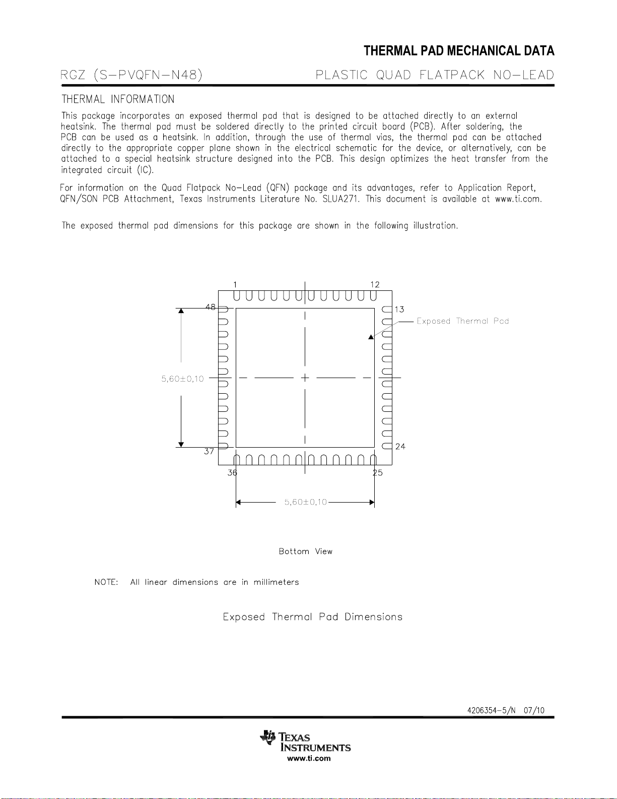

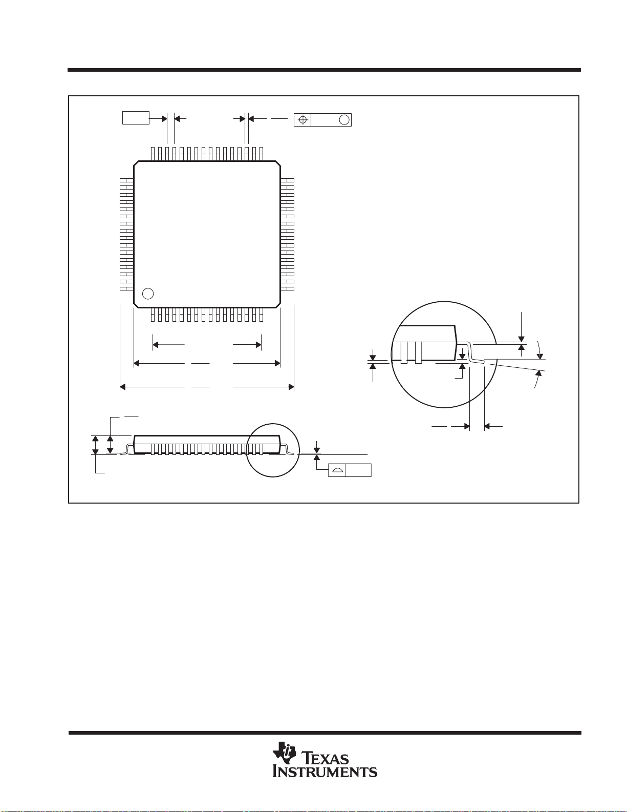
MECHANICAL DATA
MTQF006A – JANUARY 1995 – REVISED DECEMBER 1996
PAG (S-PQFP-G64) PLASTIC QUAD FLATPACK
49
64
0,50
1,05
0,95
48
0,27
0,17
33
32
17
1
7,50 TYP
10,20
SQ
9,80
12,20
SQ
11,80
16
M
0,08
0,05 MIN
Seating Plane
0,13 NOM
Gage Plane
0,25
0°–7°
0,75
0,45
1,20 MAX
NOTES: A. All linear dimensions are in millimeters.
B. This drawing is subject to change without notice.
C. Falls within JEDEC MS-026
0,08
4040282/C 11/96
POST OFFICE BOX 655303 • DALLAS, TEXAS 75265

IMPORTANT NOTICE
Texas Instruments Incorporated and its subsidiaries (TI) reserve the right to make corrections, modifications, enhancements, improvements,
and other changes to its products and services at any time and to discontinue any product or service without notice. Customers should
obtain the latest relevant information before placing orders and should verify that such information is current and complete. All products are
sold subject to TI’s terms and conditions of sale supplied at the time of order acknowledgment.
TI warrants performance of its hardware products to the specifications applicable at the time of sale in accordance with TI’s standard
warranty. Testing and other quality control techniques are used to the extent TI deems necessary to support this warranty. Except where
mandated by government requirements, testing of all parameters of each product is not necessarily performed.
TI assumes no liability for applications assistance or customer product design. Customers are responsible for their products and
applications using TI components. To minimize the risks associated with customer products and applications, customers should provide
adequate design and operating safeguards.
TI does not warrant or represent that any license, either express or implied, is granted under any TI patent right, copyright, mask work right,
or other TI intellectual property right relating to any combination, machine, or process in which TI products or services are used. Information
published by TI regarding third-party products or services does not constitute a license from TI to use such products or services or a
warranty or endorsement thereof. Use of such information may require a license from a third party under the patents or other intellectual
property of the third party, or a license from TI under the patents or other intellectual property of TI.
Reproduction of TI information in TI data books or data sheets is permissible only if reproduction is without alteration and is accompanied
by all associated warranties, conditions, limitations, and notices. Reproduction of this information with alteration is an unfair and deceptive
business practice. TI is not responsible or liable for such altered documentation. Information of third parties may be subject to additional
restrictions.
Resale of TI products or services with statements different from or beyond the parameters stated by TI for that product or service voids all
express and any implied warranties for the associated TI product or service and is an unfair and deceptive business practice. TI is not
responsible or liable for any such statements.
TI products are not authorized for use in safety-critical applications (such as life support) where a failure of the TI product would reasonably
be expected to cause severe personal injury or death, unless officers of the parties have executed an agreement specifically governing
such use. Buyers represent that they have all necessary expertise in the safety and regulatory ramifications of their applications, and
acknowledge and agree that they are solely responsible for all legal, regulatory and safety-related requirements concerning their products
and any use of TI products in such safety-critical applications, notwithstanding any applications-related information or support that may be
provided by TI. Further, Buyers must fully indemnify TI and its representatives against any damages arising out of the use of TI products in
such safety-critical applications.
TI products are neither designed nor intended for use in military/aerospace applications or environments unless the TI products are
specifically designated by TI as military-grade or "enhanced plastic." Only products designated by TI as military-grade meet military
specifications. Buyers acknowledge and agree that any such use of TI products which TI has not designated as military-grade is solely at
the Buyer's risk, and that they are solely responsible for compliance with all legal and regulatory requirements in connection with such use.
TI products are neither designed nor intended for use in automotive applications or environments unless the specific TI products are
designated by TI as compliant with ISO/TS 16949 requirements. Buyers acknowledge and agree that, if they use any non-designated
products in automotive applications, TI will not be responsible for any failure to meet such requirements.
Following are URLs where you can obtain information on other Texas Instruments products and application solutions:
Products Applications
Amplifiers amplifier.ti.com Audio www.ti.com/audio
Data Converters dataconverter.ti.com Automotive www.ti.com/automotive
DLP® Products www.dlp.com Communications and www.ti.com/communications
DSP dsp.ti.com Computers and www.ti.com/computers
Clocks and Timers www.ti.com/clocks Consumer Electronics www.ti.com/consumer-apps
Interface interface.ti.com Energy www.ti.com/energy
Logic logic.ti.com Industrial www.ti.com/industrial
Power Mgmt power.ti.com Medical www.ti.com/medical
Microcontrollers microcontroller.ti.com Security www.ti.com/security
RFID www.ti-rfid.com Space, Avionics & www.ti.com/space-avionics-defense
RF/IF and ZigBee® Solutions www.ti.com/lprf Video and Imaging www.ti.com/video
Mailing Address: Texas Instruments, Post Office Box 655303, Dallas, Texas 75265
Copyright © 2010, Texas Instruments Incorporated
Telecom
Peripherals
Defense
Wireless www.ti.com/wireless-apps
 Loading...