

Texas Instruments CD4049UBPWR, CD4049UBPW, CD4049UBNSR, CD4049UBNS, CD4050BPWR Datasheet
...
1
CAUTION: These devices are sensitive to electrostatic discharge; follow proper IC Handling Procedures.
Copyright
© 1999, Texas Instruments Incorporated
Data sheet acquired from Harris Semiconductor
SCHS046A
CD4049UB, CD4050B
CMOS Hex Buffer/Converters
The CD4049UB and CD4050B devices are inverting and
non-inverting hex buffers, respectively, and feature logiclevel conversion using only one supply voltage (V
CC
). The
input-signal high level (V
IH
) can exceed the VCC supply
voltage when these devices are used for logic-level
conversions.These devices are intended for use as CMOS
to DTL/TTL converters and can drive directly two DTL/TTL
loads. (V
CC
= 5V, VOL≤ 0.4V, and IOL≥ 3.3mA.)
The CD4049UB and CD4050B are designated as
replacements for CD4009UB and CD4010B, respectively.
Because the CD4049UB and CD4050B require only one
power supply, they are preferred over the CD4009UB and
CD4010B and should be used in place of the CD4009UB
and CD4010B in all inverter, current driver, or logic-level
conversion applications. In these applications the
CD4049UB and CD4050B are pin compatible with the
CD4009UB and CD4010B respectively, and can be
substituted for these devices in existing as well as in new
designs. Terminal No. 16 is not connected internally on the
CD4049UB or CD4050B, therefore, connection to this
terminal is of no consequence to circuit operation. For
applications not requiring high sink-current or voltage
conversion, the CD4069UB Hex Inverter is recommended.
Features
• CD4049UB Inverting
• CD4050B Non-Inverting
• High Sink Current for Driving 2 TTL Loads
• High-To-Low Level Logic Conversion
• 100% Tested for Quiescent Current at 20V
• Maximum Input Current of 1µA at 18V Over Full Package
Temperature Range; 100nA at 18V and 25
o
C
• 5V, 10V and 15V Parametric Ratings
Applications
• CMOS to DTL/TTL Hex Converter
• CMOS Current “Sink” or “Source” Driver
• CMOS High-To-Low Logic Level Converter
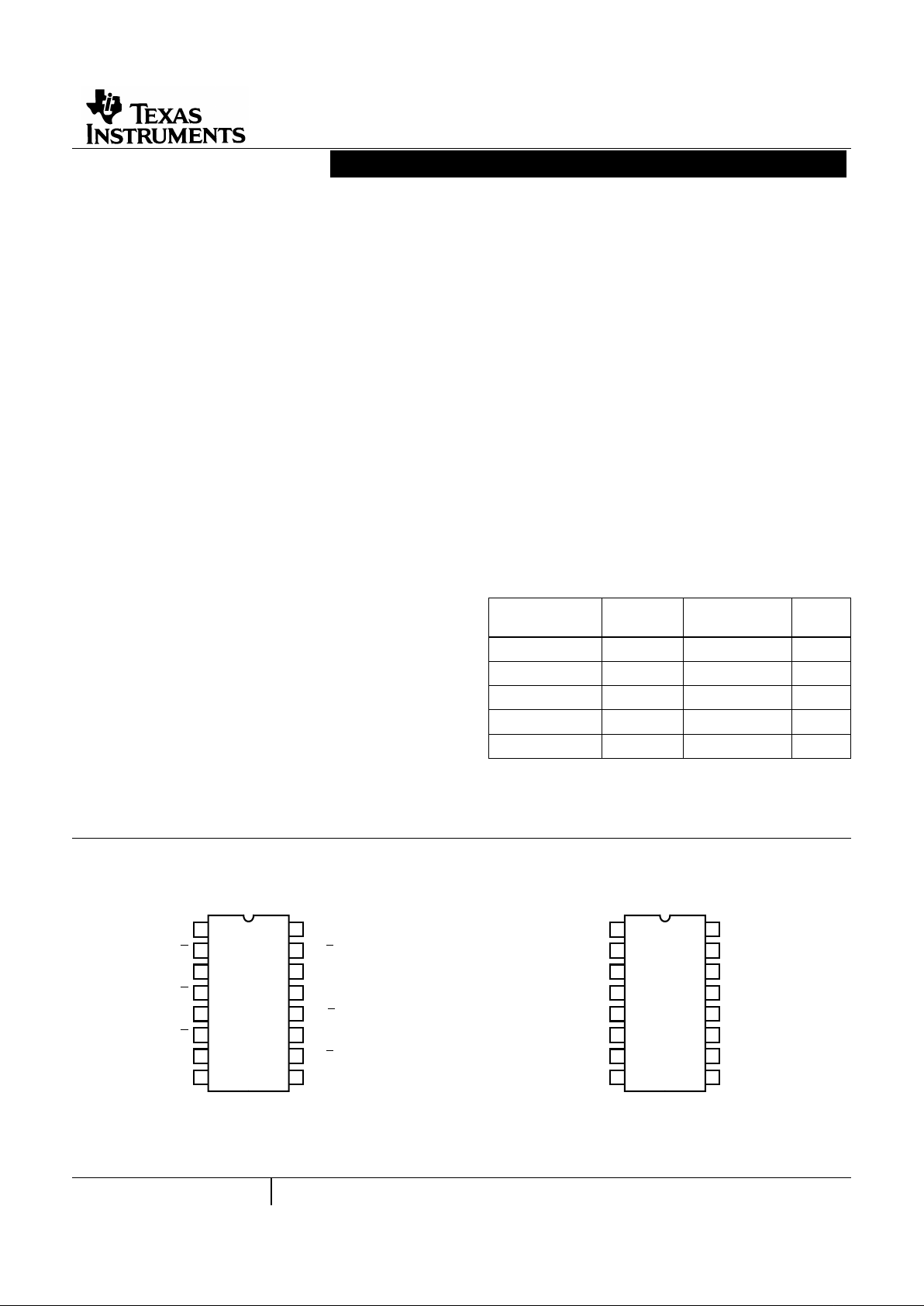
Pinouts
Ordering Information
PART NUMBER
TEMP.
RANGE (oC) PACKAGE
PKG.
NO.
CD4049UBE -55 to 125 16 Ld PDIP E16.3
CD4050BE -55 to 125 16 Ld PDIP E16.3
CD4049UBF -55 to 125 16 Ld CERDIP F16.3
CD4050BF -55 to 125 16 Ld CERDIP F16.3
CD4050BM -55 to 125 16 Ld SOIC M16.3
NOTE: Wafer and die for this part number is available which meets
all electrical specifications. Please contact your local sales office or
customer service for ordering information.
CD4049UB (PDIP, CERDIP)
TOP VIEW
CD4050B (PDIP, CERDIP, SOIC)
TOP VIEW
14
15
16
9
13
12
11
10
1
2
3
4
5
7
6
8
V
CC
G = A
A
H =
B
B
I =
C
V
SS
C
NC
F
NC
K =
E
E
J = D
D
L =
F
14
15
16
9
13
12
11
10
1
2
3
4
5
7
6
8
V
CC
G = A
A
H = B
B
I = C
V
SS
C
NC
F
NC
K = E
E
J = D
D
L = F
August 1998 - Revised May 1999
[ /Title
(CD40
49UB,
CD405
0B)
/Subject
(CMO
S Hex
Buffer/
Converters)
/Autho
r ()
/Keywords
(Harris
Semiconductor,
CD400
0,
metal
gate,
CMOS
2
Functional Block Diagrams
CD4049UB CD4050B
32
AG =
A
54
BH =
B
76
CI =
C
910
DJ =
D
11 12
EK =
E
14 15
FL =
F
1
8
V
CC
V
SS
NC = 13
NC = 16
32
A G = A
54
B H = B
76
C I = C
910
D J = D
11 12
E K = E
14 15
F L = F
1
8
V
CC
V
SS
NC = 13
NC = 16
Schematic Diagrams
FIGURE 1A. SCHEMATIC DIAGRAM OF CD4049UB, 1 OF 6
IDENTICAL UNITS
FIGURE 1B. SCHEMATIC DIAGRAM OF CD4050B, 1 OF 6
IDENTICAL UNITS
V
CC
OUT
V
SS
P
N
R
IN
P
N
R
IN
V
CC
OUT
V
SS
P
N
CD4049UB, CD4050B
3
Absolute Maximum Ratings Thermal Information
Supply Voltage (V+ to V-). . . . . . . . . . . . . . . . . . . . . . . -0.5V to 20V
DC Input Current, Any One Input. . . . . . . . . . . . . . . . . . . . . . ±10mA
Operating Conditions
Temperature Range . . . . . . . . . . . . . . . . . . . . . . . . . -55oC to 125oC
Thermal Resistance (Typical, Note 1) θJA (oC/W) θJC (oC/W)
PDIP Package . . . . . . . . . . . . . . . . . . . 90 N/A
CERDIP Package. . . . . . . . . . . . . . . . . 130 55
SOIC Package . . . . . . . . . . . . . . . . . . . 100 N/A
Maximum Junction Temperature (Plastic Package) . . . . . . . .150oC
Maximum Storage Temperature Range. . . . . . . . . . -65oC to 150oC
Maximum Lead Temperature (Soldering 10s) . . . . . . . . . . . . .265oC
(SOIC - Lead Tips Only)
CAUTION: Stresses above those listed in “Absolute Maximum Ratings” may cause permanent damage to the device. This is a stress only rating and operationofthe
device at these or any other conditions above those indicated in the operational sections of this specification is not implied.
NOTE:
1. θJA is measured with the component mounted on an evaluation PC board in free air.
DC Electrical Specifications
PARAMETER
TEST CONDITIONS
LIMITS AT INDICATED TEMPERATURE (oC)
UNITS-55 -40 85 125
25
V
O
(V)
V
IN
(V) VCC (V) MIN TYP MAX
Quiescent Device Current
IDD (Max)
- 0,5 5 1 1 30 30 - 0.02 1 µA
- 0,10 10 2 2 60 60 - 0.02 2 µA
- 0,15 15 4 4 120 120 - 0.02 4 µA
- 0,20 20 20 20 600 600 - 0.04 20 µA
Output Low (Sink) Current
IOL (Min)
0.4 0,5 4.5 3.3 3.1 2.1 1.8 2.6 5.2 - mA
0.4 0,5 5 4 3.8 2.9 2.4 3.2 6.4 - mA
0.5 0,10 10 10 9.6 6.6 5.6 8 16 - mA
1.5 0,15 15 26 25 20 18 24 48 - mA
Output High (Source) Current
IOH (Min)
4.6 0,5 5 -0.81 -0.73 -0.58 -0.48 -0.65 -1.2 - mA
2.5 0,5 5 -2.6 -2.4 -1.9 -1.55 -2.1 -3.9 - mA
9.5 0,10 10 -2.0 -1.8 -1.35 -1.18 -1.65 -3.0 - mA
13.5 0,15 15 -5.2 -4.8 -3.5 -3.1 -4.3 -8.0 - mA
Out Voltage Low Level
VOL (Max)
- 0,5 5 0.05 0.05 0.05 0.05 - 0 0.05 V
- 0,10 10 0.05 0.05 0.05 0.05 - 0 0.05 V
- 0,15 5 0.05 0.05 0.05 0.05 - 0 0.05 V
Output Voltage High Level
VOH (Min)
- 0,5 5 4.95 4.95 4.95 4.95 4.95 5 - V
- 0,10 10 9.95 9.95 9.95 9.95 9.95 10 - V
- 0,15 15 14.95 14.95 14.95 14.95 14.95 15 - V
Input Low Voltage, VIL (Max)
CD4049UB
4.5 - 5 1 1 1 1 - - 1 V
9-102222--2V
13.5 - 15 2.5 2.5 2.5 2.5 - - 2.5 V
Input Low Voltage, VIL (Max)
CD4050B
0.5 - 5 1.5 1.5 1.5 1.5 - - 1.5 V
1-103333--3V
1.5 - 154444--4 V
Input High Voltage, VIH Min
CD4049UB
0.5 - 5 4 4 4 4 4 - - V
1-1088888--V
1.5 - 15 12.5 12.5 12.5 12.5 12.5 - - V
CD4049UB, CD4050B
4
Input High Voltage, VIH Min
CD4050B
4.5 - 5 3.5 3.5 3.5 3.5 3.5 - - V
9-1077777--V
13.5 - 15 11 11 11 11 11 - - V
Input Current, IIN Max - 0,18 18 ±0.1 ±0.1 ±1 ±1-±10-5±0.1 µA
DC Electrical Specifications (Continued)
PARAMETER
TEST CONDITIONS
LIMITS AT INDICATED TEMPERATURE (
o
C)
UNITS-55 -40 85 125
25
V
O
(V)
V
IN
(V) VCC (V) MIN TYP MAX
AC Electrical Specifications T
A
= 25oC, Input tr, tf = 20ns, CL = 50pF, RL = 200kΩ
PARAMETER
TEST CONDITIONS LIMITS (ALL PACKAGES)
UNITSV
IN
V
CC
TYP MAX
Propagation Delay Time
Low to High, t
PLH
CD4049UB
5 5 60 120 ns
10 10 32 65 ns
1054590ns
15 15 25 50 ns
1554590ns
Propagation Delay Time
Low to High, t
PLH
CD4050B
5 5 70 140 ns
10 10 40 80 ns
1054590ns
15 15 30 60 ns
1554080ns
Propagation Delay Time
High to Low, t
PHL
CD4049UB
5 5 32 65 ns
10 10 20 40 ns
1051530ns
15 15 15 30 ns
1551020ns
Propagation Delay Time
High to Low, t
PHL
CD4050B
5 5 55 110 ns
10 10 22 55 ns
10 5 50 100 ns
15 15 15 30 ns
15 5 50 100 ns
Transition Time, Low to High, t
TLH
5 5 80 160 ns
10 10 40 80 ns
15 15 30 60 ns
Transition Time, High to Low, t
THL
5 5 30 60 ns
10 10 20 40 ns
15 15 15 30 ns
Input Capacitance, C
IN
CD4049UB
- - 15 22.5 pF
Input Capacitance, C
IN
CD4050B
- - 5 7.5 pF
CD4049UB, CD4050B

5
Typical Performance Curves
FIGURE 2. MINIMUM AND MAXIMUM VOLTAGE TRANSFER
CHARACTERISTICS FOR CD4049UB
FIGURE 3. MINIMUM AND MAXIMUM VOLTAGE TRANSFER
CHARACTERISTICS FOR CD4050B
FIGURE 4. TYPICAL OUTPUT LOW (SINK) CURRENT
CHARACTERISTICS
FIGURE 5. MINIMUM OUTPUT LOW (SINK) CURRENT DRAIN
CHARACTERISTICS
FIGURE 6. TYPICAL OUTPUT HIGH (SOURCE) CURRENT
CHARACTERISTICS
FIGURE 7. MINIMUM OUTPUT HIGH (SOURCE) CURRENT
CHARACTERISTICS
5
4
3
2
1
01234
V
I
, INPUT VOLTAGE (V)
V
O
, OUTPUT VOLTAGE (V)
TA = 25oC
SUPPLY VOLTAGE (VCC) = 5V
MAXIMUMMINIMUM
5
4
3
2
1
01234
V
I
, INPUT VOLTAGE (V)
V
O
, OUTPUT VOLTAGE (V)
TA = 25oC
SUPPLY VOLTAGE (VCC) = 5V
MAXIMUMMINIMUM
50
40
30
20
10
01234
V
DS
, DRAIN TO SOURCE VOLTAGE (V)
I
OL
, OUTPUT LOW (SINK) CURRENT (mA)
TA = 25oC
GATE TO SOURCE VOLTAGE (VGS) = 5V
10V
15V
60
70
5678
50
40
30
20
10
01234
VDS, DRAIN TO SOURCE VOLTAGE (V)
I
OL
, OUTPUT LOW (SINK) CURRENT (mA)
TA = 25oC
GATE TO SOURCE VOLTAGE (VGS) = 5V
10V15V
60
70
5678
-5
-10
-15
-20
-25
-30
-35
OUTPUT HIGH (SOURCE)
CURRENT CHARACTERISTICS
-15V
-10V
GATE TO SOURCE VOLTAGE
V
GS
= -5V
TA = 25oC
-8 -7 -6 -5 -4 -3 -2 -1 0
V
DS
, DRAIN TO SOURCE VOLTAGE (V)
-5
-10
-15
-20
-25
-30
-35
OUTPUT HIGH (SOURCE)
CURRENT CHARACTERISTICS
-15V
-10V
GATE TO SOURCE VOLTAGE
VGS = -5V
TA = 25oC
-8 -7 -6 -5 -4 -3 -2 -1 0
V
DS
, DRAIN TO SOURCE VOLTAGE (V)
CD4049UB, CD4050B

6
FIGURE 8. TYPICALV OLTA GETRANSFER CHARACTERISTICS
AS A FUNCTION OF TEMPERA TURE FOR CD4049UB
FIGURE 9. TYPICAL VOLTAGE TRANSFER CHARACTERISTICS
AS A FUNCTION OF TEMPERA TURE FOR CD4050B
FIGURE 10. TYPICAL POWER DISSIPATION vs FREQUENCY
CHARACTERISTICS
FIGURE 11. TYPICAL POWER DISSIPATION vs INPUT RISE
AND FALL TIMES PER INVERTER FOR CD4049UB
FIGURE 12. TYPICAL POWER DISSIPATION vs INPUT RISE
AND FALL TIMES PER INVERTER FOR CD4050B
Typical Performance Curves
(Continued)
10
6
5
4
3
2
1
V
O
, OUTPUT VOLTAGE (V)
-55oC
125oC
SUPPLY VOLTAGE
V
CC
= 10V
TA = -55oC
876543210
V
I
, INPUT VOLTAGE (V)
910
9
8
7
0
125oC
VCC = 5V
10
6
5
4
3
2
1
V
O
, OUTPUT VOLTAGE (V)
-55oC
125oC
SUPPLY VOLTAGE
V
CC
= 10V
TA = -55oC
876543210
V
I
, INPUT VOLTAGE (V)
910
9
8
7
0
125oC
VCC = 5V
10
5
10
4
10
3
10
2
10
10
10
2
10
3
10
4
10
5
TA = 25oC
SUPPLY VOLTAGE V
CC
= 15V
10V
10V
5V
LOAD CAPACITANCE
C
L
= 50pF
(11pF FIXTURE + 39pF EXT)
(11pF FIXTURE + 4pF EXT)
C
L
= 15pF
POWER DISSIPATION PER INVERTER (µW)
f, INPUT FREQUENCY (kHz)
10
5
10
4
10
3
10
2
10
10
10
2
10
3
10
4
10
5
TA = 25oC
POWER DISSIPATION PER INVERTER (µW)
tr, tf, INPUT RISE AND FALL TIME (ns)
SUPPLY VOLTAGE VCC = 5V FREQUENCY (f) = 10kHz
15V; 1MHz
15V; 100kHz
10V; 100kHz
15V; 10kHz
10V; 10kHz
15V; 1kHz
10
6
10
7
10
8
10
6
10
4
10
3
10
2
1
10 10
2
10310410
5
TA = 25oC
POWER DISSIPATION PER INVERTER (µW)
tr, tf, INPUT RISE AND FALL TIME (ns)
SUPPLY VOLTAGE VCC = 5V FREQUENCY (f) = 10kHz
10610
7
10
8
10
10
5
15V; 1MHz
15V; 100kHz
10V; 100kHz
15V; 10kHz
10V; 10kHz
15V; 1kHz
CD4049UB, CD4050B
7
Test Circuits
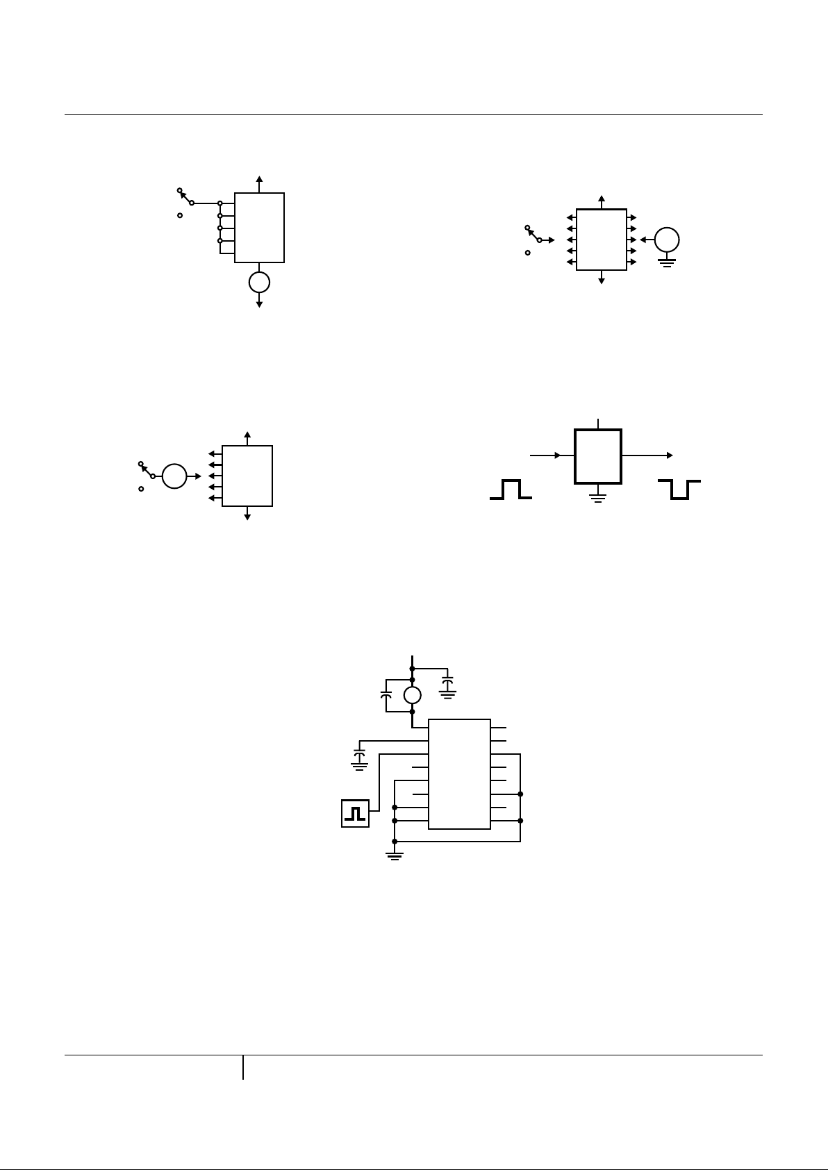
FIGURE 13. QUIESCENT DEVICE CURRENT TEST CIRCUIT
NOTE: Test any one input with other inputs at V
CC
or VSS.
FIGURE 14. INPUT VOLTAGE TEST CIRCUIT
NOTE: Measure inputs sequentially, to both V
CC
and VSS connect
all unused inputs to either VCC or VSS.
FIGURE 15. INPUT CURRENT TEST CIRCUIT
In Terminal - 3, 5, 7, 9, 11, or 14
Out Terminal - 2, 4, 6, 10, 12 or 15
VCC Terminal - 1
VSS Terminal - 8
FIGURE 16. LOGIC LEVEL CONVERSION APPLICATION
FIGURE 17. DYNAMIC POWER DISSIPATION TEST CIRCUITS
I
DD
V
CC
INPUTS
V
SS
V
CC
V
SS
V
CC
OUTPUTSINPUTS
V
IH
V
IL
V
SS
DVM
+
-
V
CC
OUTPUTSINPUTS
V
CC
V
SS
V
SS
I
VCC = 5V
OUTPUT
INPUTS
10V = V
IH
0 = V
IL
V
SS
TO DTL/TTL
CMOS 10V LEVEL TO DTL/TTL 5V LEVEL
COS/MOS
IN
0 = V
OL
5V = V
OH
CD4049
I
V
DD
500µF
0.1µF
C
L
10kHz,
100kHz, 1MHz
1
2
3
4
5
6
7
8
CD4049UB
16
15
14
13
12
11
10
9
C
L
INCLUDES FIXTURE CAPACITANCE
CD4049UB, CD4050B

8
CD4049UB, CD4050B
Dual-In-Line Plastic Packages (PDIP)
NOTES:
1. Controlling Dimensions:INCH.In caseofconflict betweenEnglishand
Metric dimensions, the inch dimensions control.
2. Dimensioning and tolerancing per ANSI Y14.5M-1982.
3. Symbols are defined in the “MO Series Symbol List” in Section 2.2 of
Publication No. 95.
4. Dimensions A, A1 and L are measured with the package seatedinJEDEC seating plane gauge GS-3.
5. D, D1, and E1 dimensions do not include mold flash or protrusions.
Mold flash or protrusions shall not exceed 0.010 inch (0.25mm).
6. E and are measured with the leads constrained to beperpendicular to datum .
7. eBand eCare measuredatthe lead tips with theleadsunconstrained.
eC must be zero or greater.
8. B1 maximum dimensions do not include dambarprotrusions.Dambar
protrusions shall not exceed 0.010 inch (0.25mm).
9. N is the maximum number of terminal positions.
10. Corner leads (1, N, N/2 and N/2 + 1) for E8.3, E16.3, E18.3, E28.3,
E42.6 will have a B1 dimension of 0.030 - 0.045 inch (0.76 - 1.14mm).
e
A
-C-
C
L
E
e
A
C
e
B
e
C
-B-
E1
INDEX
1 2 3 N/2
N
AREA
SEATING
BASE
PLANE
PLANE
-C-
D1
B1
B
e
D
D1
A
A2
L
A1
-A-
0.010 (0.25) C AM BS
E16.3 (JEDEC MS-001-BB ISSUE D)
16 LEAD DUAL-IN-LINE PLASTIC PACKAGE
SYMBOL
INCHES MILLIMETERS
NOTESMIN MAX MIN MAX
A - 0.210 - 5.33 4
A1 0.015 - 0.39 - 4
A2 0.115 0.195 2.93 4.95 -
B 0.014 0.022 0.356 0.558 B1 0.045 0.070 1.15 1.77 8, 10
C 0.008 0.014 0.204 0.355 -
D 0.735 0.775 18.66 19.68 5
D1 0.005 - 0.13 - 5
E 0.300 0.325 7.62 8.25 6
E1 0.240 0.280 6.10 7.11 5
e 0.100 BSC 2.54 BSC -
e
A
0.300 BSC 7.62 BSC 6
e
B
- 0.430 - 10.92 7
L 0.115 0.150 2.93 3.81 4
N16 169
Rev. 0 12/93

9
CD4049UB, CD4050B
Ceramic Dual-In-Line Frit Seal Packages (CERDIP)
NOTES:
1. Index area:Anotchor a pinoneidentification mark shall belocated adjacent to pin one and shall be located within the shaded
area shown. The manufacturer’s identification shall not be used
as a pin one identification mark.
2. The maximum limits of lead dimensions b and c or M shall be
measured at the centroid of the finished lead surfaces, when
solder dip or tin plate lead finish is applied.
3. Dimensions b1 and c1 apply to lead basemetalonly.Dimension
M applies to lead plating and finish thickness.
4. Corner leads (1, N, N/2, andN/2+1)may beconfiguredwith a
partial lead paddle. For this configuration dimension b3 replaces
dimension b2.
5. This dimension allows for off-center lid, meniscus, and glass
overrun.
6. Dimension Q shall be measured from the seating plane to the
base plane.
7. Measure dimension S1 at all four corners.
8. N is the maximum number of terminal positions.
9. Dimensioning and tolerancing per ANSI Y14.5M - 1982.
10. Controlling dimension: INCH.
bbb C A - B
S
c
Q
L
A
SEATING
BASE
D
PLANE
PLANE
-D-
-A-
-C-
-B-
α
D
E
S1
b2
b
A
e
M
c1
b1
(c)
(b)
SECTION A-A
BASE
LEAD FINISH
METAL
eA/2
A
M
S
S
ccc C A - BMD
S
S
aaa C A - B
M
D
S S
eA
F16.3 MIL-STD-1835 GDIP1-T16 (D-2, CONFIGURATION A)
16 LEAD CERAMIC DUAL-IN-LINE FRIT SEAL PACKAGE
SYMBOL
INCHES MILLIMETERS
NOTESMIN MAX MIN MAX
A - 0.200 - 5.08 -
b 0.014 0.026 0.36 0.66 2
b1 0.014 0.023 0.36 0.58 3
b2 0.045 0.065 1.14 1.65 b3 0.023 0.045 0.58 1.14 4
c 0.008 0.018 0.20 0.46 2
c1 0.008 0.015 0.20 0.38 3
D - 0.840 - 21.34 5
E 0.220 0.310 5.59 7.87 5
e 0.100 BSC 2.54 BSC eA 0.300 BSC 7.62 BSC -
eA/2 0.150 BSC 3.81 BSC -
L 0.125 0.200 3.18 5.08 -
Q 0.015 0.060 0.38 1.52 6
S1 0.005 - 0.13 - 7
α
90
o
105
o
90
o
105
o
aaa - 0.015 - 0.38 bbb - 0.030 - 0.76 -
ccc - 0.010 - 0.25 -
M - 0.0015 - 0.038 2 , 3
N16 168
Rev. 0 4/94

10
CD4049UB, CD4050B
Small Outline Plastic Packages (SOIC)
NOTES:
1. Symbols are defined in the “MO Series Symbol List” in Section 2.2 of
Publication Number 95.
2. Dimensioning and tolerancing per ANSI Y14.5M-1982.
3. Dimension “D” does not include mold flash, protrusions or gate burrs.
Mold flash, protrusion and gate burrs shall not exceed 0.15mm (0.006
inch) per side.
4. Dimension “E” does not include interlead flash or protrusions. Interlead
flash and protrusions shall not exceed 0.25mm (0.010 inch) per side.
5. The chamfer on the body is optional. If it is not present, a visual index
feature must be located within the crosshatched area.
6. “L” is the length of terminal for soldering to a substrate.
7. “N” is the number of terminal positions.
8. Terminal numbers are shown for reference only.
9. The lead width “B”, as measured 0.36mm (0.014 inch) or greater above
the seating plane, shall not exceed a maximum value of 0.61mm (0.024
inch)
10. Controlling dimension: MILLIMETER. Converted inch dimensions are
not necessarily exact.
INDEX
AREA
E
D
N
123
-B-
0.25(0.010) C AM BS
e
-A-
L
B
M
-C-
A1
A
SEATING PLANE
0.10(0.004)
h x 45
o
C
H
0.25(0.010) BM M
α
M16.3 (JEDEC MS-013-AA ISSUE C)
16 LEAD WIDE BODY SMALL OUTLINE PLASTIC PACKAGE
SYMBOL
INCHES MILLIMETERS
NOTESMIN MAX MIN MAX
A 0.0926 0.1043 2.35 2.65 -
A1 0.0040 0.0118 0.10 0.30 -
B 0.013 0.0200 0.33 0.51 9
C 0.0091 0.0125 0.23 0.32 D 0.3977 0.4133 10.10 10.50 3
E 0.2914 0.2992 7.40 7.60 4
e 0.050 BSC 1.27 BSC H 0.394 0.419 10.00 10.65 h 0.010 0.029 0.25 0.75 5
L 0.016 0.050 0.40 1.27 6
N16 167
α
0
o
8
o
0
o
8
o
-
Rev. 0 12/93

IMPORTANT NOTICE
T exas Instruments and its subsidiaries (TI) reserve the right to make changes to their products or to discontinue
any product or service without notice, and advise customers to obtain the latest version of relevant information
to verify, before placing orders, that information being relied on is current and complete. All products are sold
subject to the terms and conditions of sale supplied at the time of order acknowledgement, including those
pertaining to warranty, patent infringement, and limitation of liability.
TI warrants performance of its semiconductor products to the specifications applicable at the time of sale in
accordance with TI’s standard warranty. Testing and other quality control techniques are utilized to the extent
TI deems necessary to support this warranty. Specific testing of all parameters of each device is not necessarily
performed, except those mandated by government requirements.
CERT AIN APPLICATIONS USING SEMICONDUCTOR PRODUCTS MAY INVOLVE POTENTIAL RISKS OF
DEATH, PERSONAL INJURY, OR SEVERE PROPERTY OR ENVIRONMENTAL DAMAGE (“CRITICAL
APPLICATIONS”). TI SEMICONDUCTOR PRODUCTS ARE NOT DESIGNED, AUTHORIZED, OR
WARRANTED TO BE SUITABLE FOR USE IN LIFE-SUPPORT DEVICES OR SYSTEMS OR OTHER
CRITICAL APPLICATIONS. INCLUSION OF TI PRODUCTS IN SUCH APPLICA TIONS IS UNDERST OOD TO
BE FULLY AT THE CUSTOMER’S RISK.
In order to minimize risks associated with the customer’s applications, adequate design and operating
safeguards must be provided by the customer to minimize inherent or procedural hazards.
TI assumes no liability for applications assistance or customer product design. TI does not warrant or represent
that any license, either express or implied, is granted under any patent right, copyright, mask work right, or other
intellectual property right of TI covering or relating to any combination, machine, or process in which such
semiconductor products or services might be or are used. TI’s publication of information regarding any third
party’s products or services does not constitute TI’s approval, warranty or endorsement thereof.
Copyright 1999, Texas Instruments Incorporated
 Loading...