Features
➤ Direct clock/calendar replace-
ment for IBM®
AT-compatible computers and
other applications
➤ Functionally compatible with the
DS1287/DS1287A and
MC146818A
➤ 114 bytes of general nonvolatile
storage
➤ Automatic backup supply and
write-protection to make external
SRAM nonvolatile
➤ Integral lithium cell and crystal
➤ 160 ns cycle time allows fast bus
operation
➤ Intel bus timing
➤ 14 bytes for clock/calendar and
control
➤ BCD or binary format for clock
and calendar data
➤ Calendar in dayofthe week, day of
the month, months,and years with
automatic leap-year adjustment
➤ Time of day in seconds, minutes,
and hours
-
12- or 24-hour format
-
Optional daylight saving
adjustment
➤ Programmable square wave out-
put
➤ Three individually maskable in-
terrupt event flags:
-
Periodic rates from 122µsto
500 ms
-
Time-of-day alarm once per
second to once per day
-
End-of-clock update cycle
➤ Better than one minute per
month clock accuracy
General Description
The CMOS bq4287 is a low-power
microprocessor peripheral providing
a time-of-day clock and 100-year calendar with alarm features and battery operation. Other features include three maskable interrupt
sources, square wave output, and
114 bytes of general nonvolatile
storage.
The bq4287 write-protects the clock,
calendar, and storage registers during power failure. The integral
backup energy source then maintains data and operates the clock
and calendar.
The bq4287 uses its integral batterybackup controller and battery to make
a standard CMOS SRAM nonvolatile
during power-fail conditions. During
power-fail, the bq4287 automatically
write-protects the external SRAM and
provides a V
CC
output sourced from its
internal battery .
The bq4287 is a fully compatible
real-time clock for IBM AT-compatible
computers and other applications.
As shipped from Benchmarq, the
backup cell is electrically isolated
from the memory. Following the first
application of V
CC
, this isolation is
broken, and the backup cell provides
data retention to the clock, internal
RAM, V
OUT
, and CE
OUT
on subse-
quent power-downs.
The bq4287 is functionally equiva-
lent to the bq4285, except that the
battery (16, 20) and crystal pins (2,
3) are not accessible. These pins are
connected internally to a coin cell
and quartz crystal. The coin cell provides 130mAh of capacity. For a
complete description of features, operating conditions, electrical characteristics, bus timing, and pin descriptions, see the bq4285 data
sheet.
1
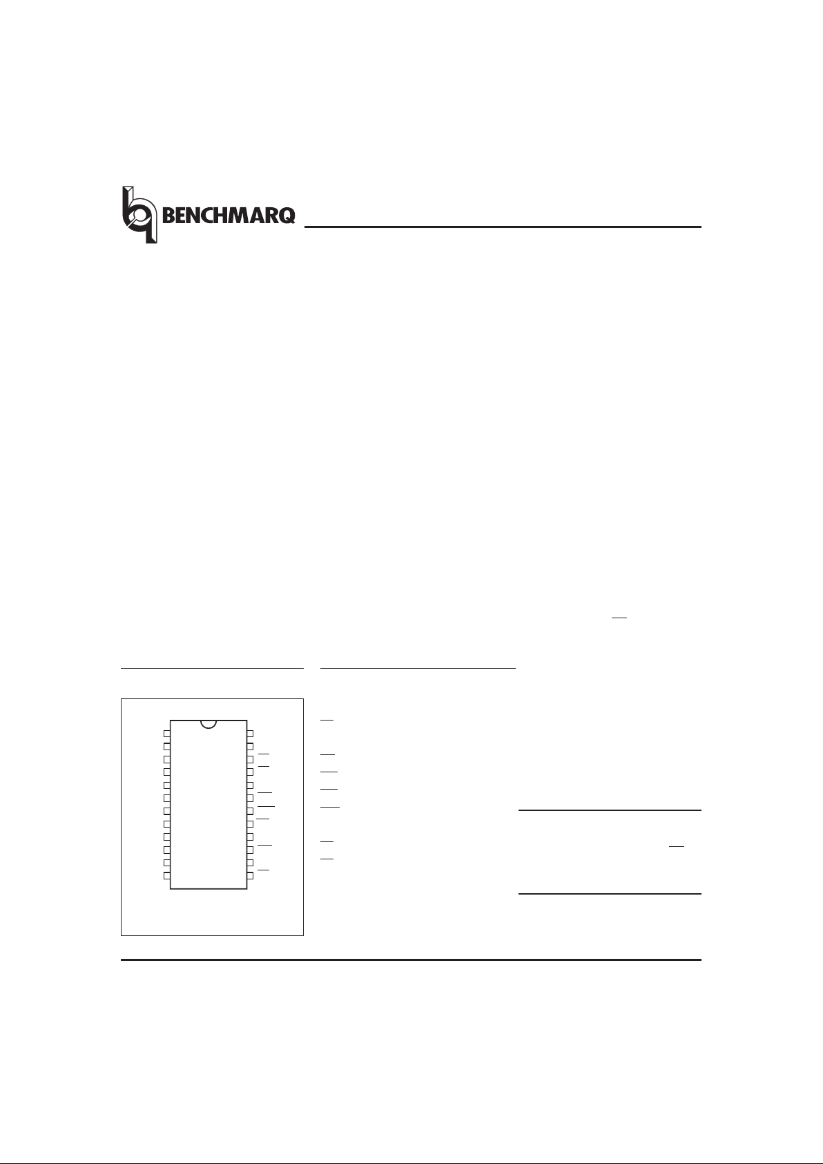
Pin Names
AD0–AD7Multiplexed address/data
input/output
CS
Chip select input
ALE Address strobe input
RD
Data strobe input
WR
Read/write input
INT
Interrupt request output
RST
Reset input
SQW Square wave output
CE
IN
RAM chip enable input
CE
OUT
RAM chip enable output
NC No connect
V
OUT
Supply output
V
CC
+5V supply
V
SS
Ground
1
PN428701.eps
24-Pin DIP Module
2
3
4
5
6
7
8
24
23
22
21
20
19
18
17
9
10
16
15
11
12
14
13
V
CC
SQW
CE
OUT
NC
INT
RST
RD
NC
WR
ALE
CS
V
OUT
NC
NC
AD
0
AD
1
AD
2
AD
3
AD
4
AD
5
AD
6
AD
7
V
SS
CE
IN
bq4287
Pin Connections
Real-Time Clock Module With NVRAM Control
Caution:
Take care to avoid inadvertent dis-
charge through V
OUT
and CE
OUT
after battery isolation has been
broken.
Nov.1993 C

2
Nov.1993 C
Recommended DC Operating Conditions (T
A=TOPR
)
Symbol Parameter Minimum Typical Maximum Unit
V
CC
Supply voltage 4.5 5.0 5.5 V
V
SS
Supply voltage 0 0 0 V
V
IL
Input low voltage -0.3 - 0.8 V
V
IH
Input high voltage 2.2 - VCC+ 0.3 V
Note: Typical values indicate operation at TA= 25°C.
DC Electrical Characteristics (T
A=TOPR,VCC
=5V±10%)
Symbol Parameter Minimum Typical Maximum Unit Conditions/Notes
C Battery capacity - 130 - mAh
Refer to graphs in Typical Battery Characteristics section
I
LI
Input leakage current - -
±
1
µ
AVIN=VSSto V
CC
I
LO
Output leakage current - -
±
1
µ
A
AD0–AD7, INT and SQW in
high impedance
V
OH
Output high voltage 2.4 - - V IOH= -1.0 mA
V
OL
Output low voltage - - 0.4 V IOL= 4.0 mA
I
CC
Operating supply current - 7 15 mA
Min. cycle, duty = 100%, I
OH
= 0mA, IOL= 0mA
I
CCB
Battery operation current - 0.3 0.5
µ
A
VBC=3V,TA= 25°C,no load
on V
OUT
or CE
OUT
V
SO
Supply switch-over voltage - 3.0 - V
V
PFD
Power-fail-detectvoltage 4.0 4.17 4.35 V
V
BC
Backup cell voltage - 3.0 - V
Internal backup cell voltage;
refer to graphs in Typical Battery Characteristics section
V
OUT1VOUT
voltage VCC- 0.3V - - V I
OUT
= 100mA, VCC>V
BC
V
OUT2VOUT
voltage VBC- 0.3V - - V I
OUT
= 100µA, VCC<V
BC
I
CE
Chip enable input current - - 100
µ
A Internal 50K pull-up
Note: Typical values indicate operation at TA= 25°C,VCC=5V.
Absolute Maximum Ratings
Symbol Parameter Value Unit Conditions
V
CC
DC voltage applied on VCCrelative to V
SS
-0.3 to 7.0 V
V
T
DC voltage applied on any pin excluding V
CC
relative to V
SS
-0.3 to 7.0 V V
T
≤
V
CC
+ 0.3
T
OPR
Operating temperature 0 to +70 °C Commercial
T
STG
Storage temperature -40 to +70 °C Commercial
T
BIAS
Temperature under bias -10 to +70 °C Commercial
T
SOLDER
Soldering temperature 260 °C For 10 seconds
Note: Permanent device damage may occur if Absolute Maximum Ratings are exceeded. Functional operation
should be limited to the Recommended DC Operating Conditions detailed in this data sheet. Exposure to conditions beyond the operational limits for extended periods of time may affect device reliability.
bq4287

3
Nov.1993 C
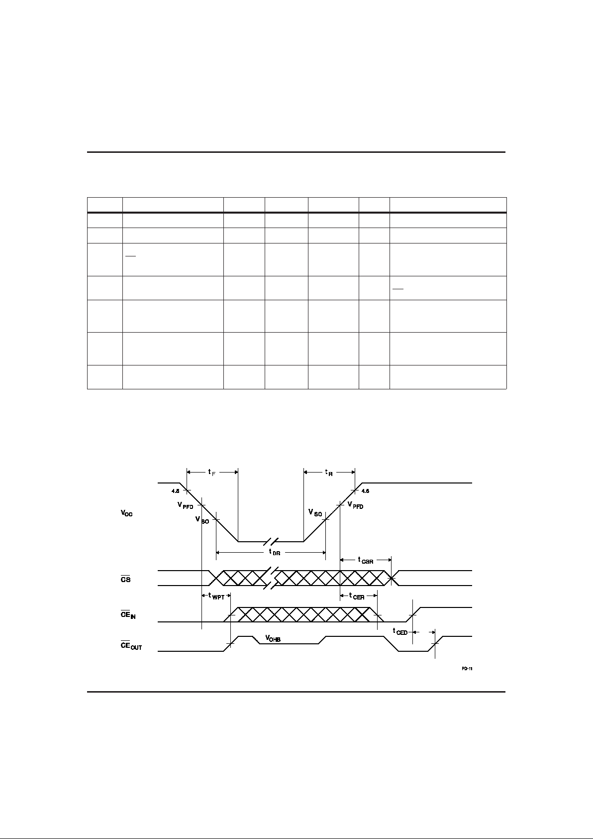
Power-Down/Power-Up Timing (T
A=TOPR)
Symbol Parameter Minimum Typical Maximum Unit Conditions
t
F
VCCslew from 4.5V to 0V 300 - -
µ
s
t
R
VCCslew from 0V to 4.5V 100 - -
µ
s
t
CSR
CS at VIHafter power-up 20 - 200 ms
Internal write-protection
period after VCCpasses V
PFD
on power-up.
t
DR
Data-retention and timekeeping time
10 - - years
TA= 25°C,no load on V
OUT
or
CE
OUT
.
t
WPT
Write-protect time for
external RAM
10 16 30
µ
s
Delay after VCCslows down
past V
PFD
before SRAM is
write-protected.
t
CER
Chip enable recovery time t
CSR
-t
CSR
ms
Time during which external
SRAM is write-protected after
VCCpasses V
PFD
on power-up.
t
CED
Chip enable propagation
delay to external SRAM
- 7 10 ns
Note: Clock accuracy is better than±1 minute per month at 25°C for the period of tDR.
Caution: Negative undershoots below the absolute maximum rating of -0.3V in battery-backup mode
may affect data integrity.
Power-Down/Power-Up Timing
bq4287
 Loading...