

Page 1
User's Guide
SLUUBL3A–June 2017–Revised October 2017
bq25606 PWR772 Evaluation Module
This user's guide provides detailed testing instructions for the bq25606 evaluation module (EVM). Also
included are descriptions of the necessary equipment, equipment setup, test procedures, the printedcircuit board layouts, schematics, and the bill of materials (BOM).
Throughout this user's guide, the abbreviations EVM, bq25606EVM, PWR772, and the term evaluation
module are synonymous with the bq25606 evaluation module, unless otherwise noted.
Contents
1 Introduction ................................................................................................................... 2
1.1 EVM Features....................................................................................................... 2
1.2 I/O Descriptions ..................................................................................................... 2
2 Test Summary................................................................................................................ 3
2.1 Equipment ........................................................................................................... 3
2.2 Equipment Setup.................................................................................................... 3
2.3 Test Procedure...................................................................................................... 5
3 PCB Layout Guideline....................................................................................................... 6
4 Board Layout ................................................................................................................. 7
5 Schematic..................................................................................................................... 9
6 Bill of Materials ............................................................................................................. 10
1 Original Test Setup for bq25606 EVM.................................................................................... 4
2 bq25606EVM Top Overlay ................................................................................................. 7
3 bq25606EVM Top Solder Mask............................................................................................ 7
4 bq25606EVM Top Layer ................................................................................................... 7
5 bq25606EVM Signal Layer 1 .............................................................................................. 7
6 bq25606EVM Signal Layer 2 .............................................................................................. 7
7 bq25606EVM Bottom Layer ............................................................................................... 7
8 bq25606EVM Bottom Solder Mask........................................................................................ 8
9 bq25606EVM Bottom Overlay ............................................................................................. 8
10 Schematic for bq25606EVM-772.......................................................................................... 9
1 Device Data Sheets ......................................................................................................... 2
2 EVM Connections............................................................................................................ 2
3 EVM Jumper Connections and Shunt Installation....................................................................... 2
4 Recommended Operating Conditions..................................................................................... 3
5 bq25606EVM-772 BOM ................................................................................................... 10
Trademarks
All trademarks are the property of their respective owners.
List of Figures
List of Tables
SLUUBL3A–June 2017–Revised October 2017
Submit Documentation Feedback
Copyright © 2017, Texas Instruments Incorporated
bq25606 PWR772 Evaluation Module
1
Page 2
Introduction
1 Introduction
1.1 EVM Features
For detailed features and operation, refer to Table 1 for a list of devices and their data sheets.
Device Data Sheet EVM Label Variant
bq25606 SLUSCK6 BQ25606EVM-772 004
The bq25606 evaluation module (EVM) is a standalone charger module without I2C control.
1.2 I/O Descriptions
Table 2 lists the jumper connections available on this EVM.
Jack Description
J1-VAC Input positive terminal
J1-GND Ground Input: negative terminal (ground terminal)
J2-PMID PMID pin connection
J2-GND Ground
J4-SYS Connected to system
J4-GND Ground
J5-BATSNS_ICHG BATSNS or ICHG pin connection
J5-BAT Connected to battery pack positive node
J5-GND Ground
www.ti.com
Table 1. Device Data Sheets
Table 2. EVM Connections
J3 Output mini-USB port
J6 I2C 4-pin connector
J7 USB-TO-GPIO connector (Not populated)
Table 3 lists the EVM jumper connections.
Table 3. EVM Jumper Connections and Shunt Installation
Jack Description bq25606 Setting
JP1 PSEL pin selection Not installed
JP2 CE pin setting: pull low to enable the charge Installed
JP3 OTG pin setting: pull high to enable OTG mode Short OTG to GND
JP4 STAT, PG, CE, INT, and OTG pins pullup source (SYS or
JP5 TS pin to GND Not installed
JP6 TS resistor divider pullup source (REGN) connection Installed
JP7 Internal 10 kΩ to GND to TS pin Installed
JP8 BATSNS selection Not installed
JP9 QON and VSET pin setting Not installed
JP10 STAT pin setting Installed
JP11 Add SYS cap Not installed
JP12 SDA and PG pin setting Installed
JP13 D+ and PSEL to J3 Not Installed
JP14 D– and PG to J3 Not Installed
JP15 D– and PG pin setting Not installed
JP16 Add VBUS cap Not installed
2
bq25606 PWR772 Evaluation Module
BAT)
Copyright © 2017, Texas Instruments Incorporated
Short to SYS
SLUUBL3A–June 2017–Revised October 2017
Submit Documentation Feedback
Page 3
www.ti.com
Table 3. EVM Jumper Connections and Shunt Installation (continued)
Jack Description bq25606 Setting
JP17 Add PMID cap Not installed
JP18 Add AT cap Not installed
S1 QON control Default open
S2 Switch to short indicator LEDs Default open
Table 4 lists the recommended operating conditions for this EVM.
Symbol Description MIN TYP MAX Unit
Supply voltage, V
Battery voltage, V
I
BAT
Supply current, I
VBUS
BAT
IN
2 Test Summary
2.1 Equipment
This section includes a list of supplies required for testing this EVM.
1. Power supply: Power supply #1 (PS#1): a power supply capable of supplying 5 V at 3 A is required.
While this part can handle larger voltage and current, it is not necessary for this procedure.
2. Load #1:
• (4-quadrant supply, constant voltage < 4.5 V) A 0–20 V, 0–5 A, > 30-W system, DC electronic load
and setting as constant voltage load mode
or
• Kepco load: BOP 20–5M, DC 0 to ±20 V, 0 to ±5 A (or higher)
3. Load #2: Use with Boost Mode, VAC to GND load, 10 Ω, 5 W or greater.
4. Meters:
• Six Fluke 75 multimeters, (equivalent or better)
or
• Four equivalent voltage meters and two equivalent current meters. The current meters must be
capable of measuring 5-A+ current
Test Summary
Table 4. Recommended Operating Conditions
Input voltage from AC adapter 3.9 5.0 13.5 V
Voltage applied at V
Fast charging current 0 3.0 A
Discharging current through internal MOSFET 6.0 A
Maximum input current from AC adapter input 0 3.0 A
terminal 0 4.208 4.4 V
BAT
2.2 Equipment Setup
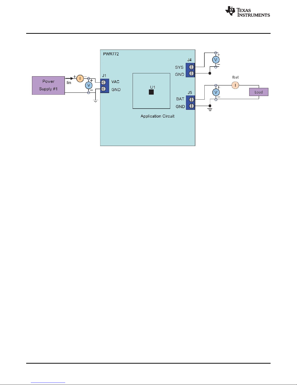
Use the following list to set up the equipment:
1. Set PS#1 for 5-V DC, 3-A current limit and then turn off the supply.
2. Connect the output of PS#1 in series with a current meter (multimeter) to J1 (VAC and GND). It is
recommended to connect one voltage meter across TP24 and TP27 to measure the input current
sensing resistor voltage. The sensing resistor is 10 mΩ.
3. Connect one voltage meter across TP21 (VAC) and TP18 (GND), connect another voltage meter
across TP1 (VBUS) and TP18 (GND).
4. Turn on Load #1, set to constant voltage mode and output to 2.5 V. Turn off (disable) load. Connect
load to J5 (BAT and GND).
5. Connect one voltage meter across TP9 (BAT) and TP17 (GND) to measure the battery voltage and
another voltage meter across TP28 and TP29 to measure the battery current sensing resistor voltage.
The sensing resistor is 10 mΩ. An alternate method is to use the optional current meter in series to
measure the battery current.
SLUUBL3A–June 2017–Revised October 2017
Submit Documentation Feedback
Copyright © 2017, Texas Instruments Incorporated
bq25606 PWR772 Evaluation Module
3
Page 4
Test Summary
6. Install shunts as shown in Table 3.
www.ti.com
Figure 1. Original Test Setup for bq25606 EVM
4
bq25606 PWR772 Evaluation Module
Copyright © 2017, Texas Instruments Incorporated
SLUUBL3A–June 2017–Revised October 2017
Submit Documentation Feedback
Page 5

www.ti.com
2.3 Test Procedure
2.3.1 Charger Mode Verification
1. Enable Load #1 from Section 2.2, Step 4.
2. Measure the voltage across J4 and J5 as follows:
• Measure → V(TP8(SYS), TP17(GND)) = 3.65 V (typical)
• Measure → V(TP9(BAT), TP17(GND)) = 2.5 V (typical)
• Measure → IBAT ( = pre-charge current)
3. Change Load #1 to 3.7 V
• Measure → V(TP8(SYS), TP17(GND)) = 3.8 V (typical)
• Measure → V(TP9(BAT), TP17(GND)) = 3.7 V (typical)
• Measure → IBAT ( = fast charge current)
4. Adjust R10 to change charging current.
5. Adjust R11 to change input current limit.
6. Turn off and disconnect Load #1.
7. Turn off and disconnect PS#1.
2.3.2 Boost Mode Verification
1. Do not install JP3.
2. If the constant voltage load connected from BAT to GND is not a four-quadrant supply (sources
current), remove the load and use the power source disconnected in step 1, set to 3.7 V and 2-A
current limit and connect between BAT and GND.
3. Apply 10 Ω (5 W or greater) across J1 VAC(+) to GND(–).
4. Verify V
Measure → V
5. Turn off and disconnect power supply.
6. Remove 10-Ω resistor at VAC.
to GND since VBUS is the actual boost mode output voltage.
VBUS
= 5.15 V (Typical)
VBUS
Test Summary
2.3.3 Helpful Tips
• The leads and cables to the various power supplies, batteries, and loads have resistance. The current
meters also have series resistance. The charger dynamically reduces charge current depending on the
voltage sensed at its VBUS pin (using the VINDPM feature), BAT pin (as part of normal termination),
and TS pin (through its battery temperature monitoring feature via battery thermistor). Therefore,
voltmeters must be used to measure the voltage as close to the IC pins as possible instead of relying
on the digital readouts of the power supply. If a battery thermistor is not available, make sure shunts
JP6 and JP7 are in place.
• When using a source meter that can source and sink current as your battery simulator, TI highly
recommends adding a large (1000+ μF) capacitor at the EVM BAT and GND connectors in order to
prevent oscillations at the BAT pin due to mismatched impedances of the charger output and source
meter input within their respective regulation loop bandwidths. Configuring the source meter for 4-wire
sensing eliminates the need for a separate voltmeter to measure the voltage at the BAT pin.
When using 4-wire sensing, always ensure that the sensing leads are connected in order to prevent
accidental overvoltage by the power leads.
• For precise measurements of charge current and battery regulation near termination, the current meter
in series with the battery or battery simulator should not be set to auto-range and may need be
removed entirely. An alternate method for measuring charge current is to either use an oscilloscope
with Hall effect current probe or place a 1% or better, thermally capable (for example, 0.010 Ω in 1210
or larger footprint) resistor in series between the BAT pin and battery and measure the voltage across
that resistor. The bq25606EVM has the sensing resistors onboard.
SLUUBL3A–June 2017–Revised October 2017
Submit Documentation Feedback
Copyright © 2017, Texas Instruments Incorporated
bq25606 PWR772 Evaluation Module
5
Page 6

PCB Layout Guideline
3 PCB Layout Guideline
Minimize the switching node rise and fall times for minimum switching loss. Proper layout of the
components minimizing high-frequency current path loop is important to prevent electrical and magnetic
field radiation and high-frequency resonant problems. This PCB layout priority list must be followed in the
order presented for proper layout:
1. Place the input capacitor as close as possible to the PMID pin and GND pin connections and use the
shortest copper trace connection or GND plane.
2. Place the inductor input terminal as close to the SW pin as possible. Minimize the copper area of this
trace to lower electrical and magnetic field radiation but make the trace wide enough to carry the
charging current. Do not use multiple layers in parallel for this connection. Minimize parasitic
capacitance from this area to any other trace or plane.
3. Put an output capacitor near to the inductor and the IC. Tie ground connections to the IC ground with a
short copper trace connection or GND plane.
4. Route analog ground separately from the power ground. Connect analog ground and connect power
ground separately. Connect analog ground and power ground together using a power pad as the
single ground connection point or use a 0-Ω resistor to tie analog ground to power ground.
5. Use a single ground connection to tie the charger power ground to the charger analog ground just
beneath the IC. Use ground copper pour but avoid power pins to reduce inductive and capacitive noise
coupling.
6. Place decoupling capacitors next to the IC pins and make the trace connection as short as possible.
7. It is critical that the exposed power pad on the backside of the IC package be soldered to the PCB
ground. Ensure that there are sufficient thermal vias directly under the IC connecting to the ground
plane on the other layers.
8. The via size and number should be enough for a given current path.
See the EVM design for the recommended component placement with trace and via locations. For the
QFN information, see Quad Flatpack No-Lead Logic Packages and QFN/SON PCB Attachment.
www.ti.com
6
bq25606 PWR772 Evaluation Module
Copyright © 2017, Texas Instruments Incorporated
SLUUBL3A–June 2017–Revised October 2017
Submit Documentation Feedback
Page 7
www.ti.com
4 Board Layout
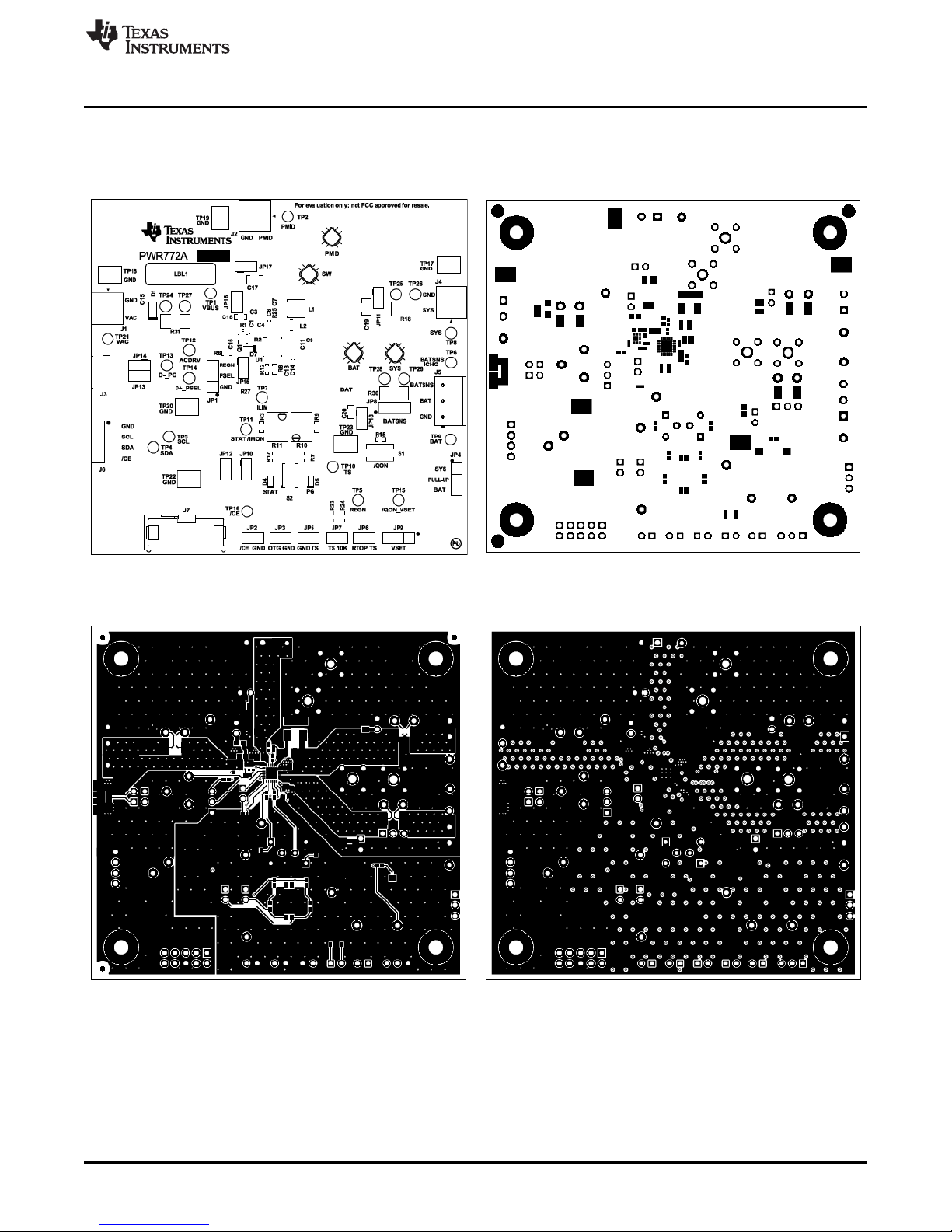
Figure 2 through Figure 9 show the EVM PCB layout images.
Board Layout
Figure 2. bq25606EVM Top Overlay Figure 3. bq25606EVM Top Solder Mask
Figure 4. bq25606EVM Top Layer Figure 5. bq25606EVM Signal Layer 1
SLUUBL3A–June 2017–Revised October 2017
Submit Documentation Feedback
Copyright © 2017, Texas Instruments Incorporated
bq25606 PWR772 Evaluation Module
7
Page 8

Board Layout
Figure 6. bq25606EVM Signal Layer 2 Figure 7. bq25606EVM Bottom Layer
www.ti.com
Figure 8. bq25606EVM Bottom Solder Mask Figure 9. bq25606EVM Bottom Overlay
8
bq25606 PWR772 Evaluation Module
Copyright © 2017, Texas Instruments Incorporated
SLUUBL3A–June 2017–Revised October 2017
Submit Documentation Feedback
Page 9

1 2
3 4
5 6
7 8
9 10
J7
DNP
0
R21
DNP
200
R19
DNP
200
R20
DNP
SDA_/PG
SCL_OTG
PGND
VBUS
1
D-
2
D+
3
ID
4
GND
5
678
11
10
9
J3
VAC
PGND
PGND
4
1
2
3
J6
PGND
SCL_OTG
SDA_/PG
/CE
D+_PSEL
PGND
VAC
GND
PMID
GND
Vbus: 3.9V to 14V
1000pF
C2
DNP
2.21kR4
10.0k
R5
DNP
JP3
/CE
AGND
AGND
TP2TP1
1µF
C1
TP3 TP4 TP7
13V
D1
DNP
2.21k
R17
30.1k
R23
10
R26
DNP
0.1µF
C11
DNP
System
GND
GND
PGND
Battery
PGND
PULL-UP
TS
GND
10µF
C9
10µF
C10
10µF
C19
DNP
20V
D3
DNP
ICHG: 0 ~ 2.5A
40V
D2
DNP
0.047µF
C7
0
R25
1
2
3
J5
TP6
BATSNS_ICHG
PGND
1µH
L1
DNP
4.7k
R15
DNP
AGND
S1
DNP
STAT_/IMON
REGN
CSD17571Q2
3
5,6,8 4,7
1,2,
Q1
DNP
0
R2
DNP
PGND
JP16
DNP
JP17
DNP
PGND
PGND
1µF
C18
DNP
SCL_OTG
SDA_/PG
VBUS PMID
VAC
VAC
SDA_/PG
D+_PSEL
D-_/PG
10k ohm
R10
PGND
/CE
10K
TS
20V
D6
DNP
J2
1
2
3
JP1
AGND
10.0k
R6
REGN
D+_PSEL
JP2
/CE
AGND
PMID
10µF
C3
DNP
10µF
C17
DNP
10µF
C4
1000pF
C5
DNP
4.7µF
C6
AGND
PMID
/QON_VSET
/QON_VSET
JP5
10.0k
R24
5.23k
R22
JP6
REGN
JP7
REGN
110pF
C8
DNP
INT_ILIM
AGND
1
234
5
SW1
DNP
PGND
1
2
3
JP4
PULL-UP
JP18
DNP
JP11
DNP
1000pF
C12
DNP
10µF
C13
4.7µF
C20
DNP
4.7µF
C14
DNP
NT1
Net-Tie
0
R16
DNP
Green
D4
REGN
RTOP TS
PSEL
GND
REGN
/CE
GND
GND
OTG
TP9
TP8
SYS
BAT
BAT
SYS
TP5
REGN BATSNS_ICHG INT_ILIMSCL_OTG
TP10 TP11
TS
TS
TP12
DNP
TP13
D-_/PG
TP14 TP15
/QON_VSETD+_PSEL
TP16
/CE
TP17 TP18 TP19 TP20
AGND
PGND
BAT
SYS
PULLUP
AGND
10k ohm
R11
PULL-UP
1
234
5
SW3
DNP
1
234
5
SW4
DNP
1
234
5
SW2
DNP
BAT
SYS
SW
PMID
JP13
SCL_OTG
1
2
3
JP9
AGND
/QON_VSET
1µF
C15
0.1µF
C16
AGND
0.005
R1
STAT_/IMON
STAT_/IMON
BATSNS_ICHG
BTST
JP10
2.21k
R7
Green
D5
JP12
SDA_/PG
TP21
VAC
0
R27
D-_/PG
10.0k
R29
PGND
D-_/PG
VBUS
AGND
JP14
JP15
DNP
10.0k
R13
DNP
PULL-UP
1
2
4
3
S2
10.0k
R14
TP22 TP23
0.01
R31
158
R12
1.00k
R3
221
R8
2.80k
R9
1
2
3
JP8
DNP
BATSNS_ICHG
BAT
BATCON
0.01
R30
40V
D7
DNP
TP24
0.01
R18
TP27
TP25 TP26
TP28
TP29
J1
J4
1µH
L2
NC
2
BAT
13
BAT
14
ICHG
10
BTST
21
PAD
25
GND
17
GND
18
PMID
23
D+
3
REGN
22
OTG
6
PG
7
STAT
5
SW
19
SW
20
SYS
15
SYS
16
TS
11
VBUS
24
VAC
1
CE
9
ILIM
8
D-
4
VSET
12
U1
BQ25606RGER
Copyright © 2017, Texas Instruments Incorporated
www.ti.com
Schematic
9
SLUUBL3A–June 2017 –Revised October 2017
Submit Documentation Feedback
Copyright © 2017, Texas Instruments Incorporated
bq25606 PWR772 Evaluation Module
5 Schematic
Figure 10 shows the schematic for the bq25606 EVM.
Figure 10. Schematic for bq25606EVM-772
Page 10

Bill of Materials
www.ti.com
10
SLUUBL3A–June 2017 –Revised October 2017
Submit Documentation Feedback
Copyright © 2017, Texas Instruments Incorporated
bq25606 PWR772 Evaluation Module
6 Bill of Materials
Table 5 lists the bq25606EVM-772 BOM.
Table 5. bq25606EVM-772 BOM
Designator Qty Value Description Package Reference Part Number Manufacturer Alternate Part
Number
Alternate
Manufacturer
!PCB 1 Printed circuit board PWR772 Any
C1 1 1 µF Capacitor, ceramic, 1 µF, 35 V, ± 10%, X5R, 0603 0603 GMK107BJ105KA-T Taiyo Yuden
C4 1 10 µF Capacitor, ceramic, 10 µF, 25 V, ± 10%, X7S, 0805 0805 GRM21BC71E106KE11L Murata
C6 1 4.7 µF Capacitor, ceramic, 4.7 µF, 16 V, ± 10%, X5R, 0603 0603 GRM188R61C475KAAJ Murata
C7 1 0.047µFCapacitor, ceramic, 0.047 µF, 25 V, ± 10%, X7R, 0402 0402 GRM155R71E473KA88D Murata
C9, C10, C13 3 10 µF Capacitor, ceramic, 10 µF, 10 V, ± 10%, X7R, 0805 0805 GRM21BR71A106KE51L Murata
C15 1 1µF Capacitor, ceramic, 1 µF, 25 V, ± 10%, X7R, 0805 0805 GRM219R71E105KA88D Murata
C16 1 0.1 µF Capacitor, ceramic, 0.1 µF, 25 V, ± 10%, X7R, 0402 0402 GRM155R71E104KE14D Murata
D4, D5 2 Green LED, Green, SMD 1.6 × 0.8 × 0.8 mm LTST-C190GKT Lite-On
J1, J2, J4 3 Connector Terminal Block, 2 POS, 3.81 mm, TH 2 POS Terminal Block 1727010 Phoenix Contact
J3 1 Connector, Receptacle, Micro-USB Type B, R/A, Bottom Mount
SMT
7.5 × 2.45 × 5 mm 0473460001 Molex
J5 1 Terminal Block Receptacle, 3 × 1, 3.81 mm, R/A, TH Term Block, 3 pos 1727023 Phoenix Contact
J6 1 Header (friction lock), 100 mil, 4x1, R/A, TH 4× 1 R/A Header 22-05-3041 Molex
JP1, JP4, JP9 3 Header,100 mil, 3 × 1, Tin, TH Header, 3 PIN, 100 mil, Tin PEC03SAAN Sullins Connector
Solutions
JP2, JP3, JP5, JP6, JP7,
JP10, JP12, JP13, JP14
9 Header, 100 mil, 2 × 1, Tin, TH Header,2 PIN, 100 mil, Tin PEC02SAAN Sullins Connector
Solutions
L2 1 1 µH Inductor, 1 µH, 3.2 A, 0.028 Ω, SMD 2.5 × 2 mm MPIM252010F1R0M-LF Microgate
LBL1 1 Thermal Transfer Printable Labels, 0.650" W × 0.200" H - 10,000
per roll
PCB Label 0.650" H × 0.200"WTHT-14-423-10 Brady
R1 1 0.005 Resistor, 0.005, 1%, 0.25 W, AEC-Q200 Grade 1, 0603 0603 ERJ3LWFR005V Panasonic
R3 1 1.00 k Resistor, 1.00 k, 1%, 0.063 W, 0402 0402 CRCW04021K00FKED Vishay-Dale
R4, R7, R17 3 2.21 k Resistor, 2.21 k, 1%, 0.063 W, 0402 0402 CRCW04022K21FKED Vishay-Dale
R6, R14, R24, R29 4 10.0 k Resistor, 10.0 k, 1%, 0.063 W, 0402 0402 CRCW040210K0FKED Vishay-Dale
R8 1 221 Resistor, 221, 1%, 0.063 W, 0402 0402 CRCW0402221RFKED Vishay-Dale
R9 1 2.80 k Resistor, 2.80 k, 1%, 0.063 W, 0402 0402 CRCW04022K80FKED Vishay-Dale
R10, R11 2 10 kΩ Trimmer, 10 kΩ, 0.25W, TH 4.5 × 8 × 6.7 mm 3266W-1-103LF Bourns
R12 1 158 Resistor, 158, 1%, 0.063 W, 0402 0402 CRCW0402158RFKED Vishay-Dale
R18, R30, R31 3 0.01 Resistor, 0.01, 1%, 1 W, 2010 2010 WSL2010R0100FEA18 Vishay-Dale
R22 1 5.23 k Resistor, 5.23 k, 1%, 0.063 W, 0402 0402 CRCW04025K23FKED Vishay-Dale
R23 1 30.1 k Resistor, 30.1 k, 1%, 0.063 W, 0402 0402 CRCW040230K1FKED Vishay-Dale
R25, R27 2 0 Resistor, 0, 5%, 0.063 W, 0402 0402 CRCW04020000Z0ED Vishay-Dale
S2 1 Switch, SPST, 2 POS, 25 mA, 24 VDC, SMD 3.71 × 5.8 mm 218-2LPST CTS Electrocomponents
SH-JP2, SH-JP3, SH-
JP4, SH-JP6, SH-JP7,
SH-JP10, SH-JP12, SHJP13, SH-JP14
9 1 × 2 Shunt, 100 mil, Gold plated, Black Shunt 969102-0000-DA 3M SNT-100-BK-G Samtec
Page 11
www.ti.com
Bill of Materials
11
SLUUBL3A–June 2017 –Revised October 2017
Submit Documentation Feedback
Copyright © 2017, Texas Instruments Incorporated
bq25606 PWR772 Evaluation Module
Table 5. bq25606EVM-772 BOM (continued)
Designator Qty Value Description Package Reference Part Number Manufacturer Alternate Part
Number
Alternate
Manufacturer
TP1, TP2 2 Test Point, Miniature, Red, TH Red Miniature Testpoint 5000 Keystone
TP3, TP4, TP6, TP7,
TP10, TP11, TP13, TP14,
TP15, TP16, TP21, TP24,
TP25, TP26, TP27, TP28,
TP29
17 Test Point, Miniature, White, TH White Miniature Testpoint 5002 Keystone
TP5, TP8 2 Test Point, Miniature, Orange, TH Orange Miniature Testpoint 5003 Keystone
TP9 1 Test Point, Miniature, Yellow, TH Yellow Miniature Testpoint 5004 Keystone
TP17, TP18, TP19, TP20,
TP22, TP23
6 Test Point, Compact, SMT Testpoint_Keystone_Compact 5016 Keystone
U1 1 BQ25606RGER, RGE0024H (VQFN-24) RGE0024H bq25606RGER Texas Instruments bq25606RGET Texas Instruments
C2, C5, C12 0 1000pFCapacitor, ceramic, 1000 pF, 50 V, ± 5%, C0G/NP0, 0402 0402 GRM1555C1H102JA01D Murata
C3, C17 0 10 µF Capacitor, ceramic, 10 µF, 25 V, ± 10%, X5R, 0805 0805 GRM21BR61E106KA73L Murata
C8 0 110 pF Capacitor, ceramic, 110 pF, 25 V, ± 5%, C0G/NP0, 0402 0402 GRM1555C1E111JA01D Murata
C11 0 0.1 µF Capacitor, ceramic, 0.1 µF, 25 V, ± 20%, X7R, 0402 0402 C1005X7R1E104M050BB TDK
C14, C20 0 4.7 µF Capacitor, ceramic, 4.7 µF, 16 V, ± 10%, X5R, 0603 0603 GRM188R61C475KAAJ Murata
C18 0 1 µF Capacitor, ceramic, 1 µF, 35 V, ± 10%, X5R, 0603 0603 GMK107BJ105KA-T Taiyo Yuden
C19 0 10 µF Capacitor, ceramic, 10 µF, 10 V, ± 10%, X7R, 0805 0805 GRM21BR71A106KE51L Murata
D1 0 13 V Diode, TVS, Uni, 13 V, W, SOD-123W SOD-123W PTVS13VS1UR,115 NXP Semiconductor
D2, D7 0 40 V Diode, Schottky, 40 V, 0.38 A, SOD-523 SOD-523 ZLLS350TA Diodes Inc.
D3, D6 0 20 V Diode, Schottky, 20 V, 1 A, 152AD 152AD NSR10F20NXT5G ON Semiconductor
FID1, FID2, FID3, FID4,
FID5, FID6
0 Fiducial mark. There is nothing to buy or mount. N/A N/A N/A
H1, H2, H3, H4 0 Machine Screw, Round, #4 - 40 × 1/4, Nylon, Philips panhead Screw NY PMS 440 0025 PH BampersandF Fastener
Supply
- -
H5, H6, H7, H8 0 Standoff, Hex, 0.5"L #4-40 Nylon Standoff 1902C Keystone - J7 0 Header (shrouded), 100 mil, 5x2, High-Temperature, Gold, TH 5 × 2 Shrouded header N2510-6002-RB 3M
JP8 0 Header, 100 mil, 3 × 1, Tin, TH Header,3 PIN, 100 mil, Tin PEC03SAAN Sullins Connector
Solutions
JP11, JP15, JP16, JP17,
JP18
0 Header, 100 mil, 2 × 1, Tin, TH Header,2 PIN, 100 mil, Tin PEC02SAAN Sullins Connector
Solutions
L1 0 1 uH Inductor, Wirewound, 1 µH, 4 A, 0.041 Ω, SMD 4.06 × 4.06 mm 74437321010 Wurth Elektronik
Q1 0 30 V MOSFET, N-CH, 30 V, 22 A, DQK0006C (WSON-6) DQK0006C CSD17571Q2 Texas Instruments
R2, R16, R21 0 0 Resistor, 0, 5%, 0.063 W, 0402 0402 CRCW04020000Z0ED Vishay-Dale
R5, R13 0 10.0 k Resistor, 10.0 k, 1%, 0.063 W, 0402 0402 CRCW040210K0FKED Vishay-Dale
R15 0 4.7 k Resistor, 4.7 k, 5%, 0.063 W, 0402 0402 CRCW04024K70JNED Vishay-Dale
R19, R20 0 200 Resistor, 200, 1%, 0.063 W, 0402 0402 CRCW0402200RFKED Vishay-Dale
R26 0 10 Resistor, 10, 5%, 0.063 W, 0402 0402 CRCW040210R0JNED Vishay-Dale
S1 0 Switch, Normally open, 2.3-N force, 200-k operations, SMD KSR KSR221GLFS CampersandK
Components
Page 12

Bill of Materials
www.ti.com
12
SLUUBL3A–June 2017 –Revised October 2017
Submit Documentation Feedback
Copyright © 2017, Texas Instruments Incorporated
bq25606 PWR772 Evaluation Module
Table 5. bq25606EVM-772 BOM (continued)
Designator Qty Value Description Package Reference Part Number Manufacturer Alternate Part
Number
Alternate
Manufacturer
SH-JP1, SH-JP5, SHJP8, SH-JP9, SH-JP11,
SH-JP15, SH-JP16, SHJP17, SH-JP18
0 1 × 2 Shunt, 100-mil, Gold plated, Black Shunt 969102-0000-DA 3M SNT-100-BK-G Samtec
SW1, SW2, SW3, SW4 0 Compact Probe Tip Circuit Board Test Points, TH, 25 per TH Scope Probe 131-5031-00 Tektronix
TP12 0 Test Point, Miniature, White, TH White Miniature Testpoint 5002 Keystone
Page 13

www.ti.com
Revision History
Revision History
NOTE: Page numbers for previous revisions may differ from page numbers in the current version.
Changes from June 2, 2017 to September 30, 2017 ....................................................................................................... Page
• Changed Schematic for bq25606EVM-772............................................................................................ 9
• Changed bq25606EVM-772 BOM..................................................................................................... 10
SLUUBL3A–June 2017–Revised October 2017
Submit Documentation Feedback
Copyright © 2017, Texas Instruments Incorporated
Revision History
13
Page 14

IMPORTANT NOTICE FOR TI DESIGN INFORMATION AND RESOURCES
Texas Instruments Incorporated (‘TI”) technical, application or other design advice, services or information, including, but not limited to,
reference designs and materials relating to evaluation modules, (collectively, “TI Resources”) are intended to assist designers who are
developing applications that incorporate TI products; by downloading, accessing or using any particular TI Resource in any way, you
(individually or, if you are acting on behalf of a company, your company) agree to use it solely for this purpose and subject to the terms of
this Notice.
TI’s provision of TI Resources does not expand or otherwise alter TI’s applicable published warranties or warranty disclaimers for TI
products, and no additional obligations or liabilities arise from TI providing such TI Resources. TI reserves the right to make corrections,
enhancements, improvements and other changes to its TI Resources.
You understand and agree that you remain responsible for using your independent analysis, evaluation and judgment in designing your
applications and that you have full and exclusive responsibility to assure the safety of your applications and compliance of your applications
(and of all TI products used in or for your applications) with all applicable regulations, laws and other applicable requirements. You
represent that, with respect to your applications, you have all the necessary expertise to create and implement safeguards that (1)
anticipate dangerous consequences of failures, (2) monitor failures and their consequences, and (3) lessen the likelihood of failures that
might cause harm and take appropriate actions. You agree that prior to using or distributing any applications that include TI products, you
will thoroughly test such applications and the functionality of such TI products as used in such applications. TI has not conducted any
testing other than that specifically described in the published documentation for a particular TI Resource.
You are authorized to use, copy and modify any individual TI Resource only in connection with the development of applications that include
the TI product(s) identified in such TI Resource. NO OTHER LICENSE, EXPRESS OR IMPLIED, BY ESTOPPEL OR OTHERWISE TO
ANY OTHER TI INTELLECTUAL PROPERTY RIGHT, AND NO LICENSE TO ANY TECHNOLOGY OR INTELLECTUAL PROPERTY
RIGHT OF TI OR ANY THIRD PARTY IS GRANTED HEREIN, including but not limited to any patent right, copyright, mask work right, or
other intellectual property right relating to any combination, machine, or process in which TI products or services are used. Information
regarding or referencing third-party products or services does not constitute a license to use such products or services, or a warranty or
endorsement thereof. Use of TI Resources may require a license from a third party under the patents or other intellectual property of the
third party, or a license from TI under the patents or other intellectual property of TI.
TI RESOURCES ARE PROVIDED “AS IS” AND WITH ALL FAULTS. TI DISCLAIMS ALL OTHER WARRANTIES OR
REPRESENTATIONS, EXPRESS OR IMPLIED, REGARDING TI RESOURCES OR USE THEREOF, INCLUDING BUT NOT LIMITED TO
ACCURACY OR COMPLETENESS, TITLE, ANY EPIDEMIC FAILURE WARRANTY AND ANY IMPLIED WARRANTIES OF
MERCHANTABILITY, FITNESS FOR A PARTICULAR PURPOSE, AND NON-INFRINGEMENT OF ANY THIRD PARTY INTELLECTUAL
PROPERTY RIGHTS.
TI SHALL NOT BE LIABLE FOR AND SHALL NOT DEFEND OR INDEMNIFY YOU AGAINST ANY CLAIM, INCLUDING BUT NOT
LIMITED TO ANY INFRINGEMENT CLAIM THAT RELATES TO OR IS BASED ON ANY COMBINATION OF PRODUCTS EVEN IF
DESCRIBED IN TI RESOURCES OR OTHERWISE. IN NO EVENT SHALL TI BE LIABLE FOR ANY ACTUAL, DIRECT, SPECIAL,
COLLATERAL, INDIRECT, PUNITIVE, INCIDENTAL, CONSEQUENTIAL OR EXEMPLARY DAMAGES IN CONNECTION WITH OR
ARISING OUT OF TI RESOURCES OR USE THEREOF, AND REGARDLESS OF WHETHER TI HAS BEEN ADVISED OF THE
POSSIBILITY OF SUCH DAMAGES.
You agree to fully indemnify TI and its representatives against any damages, costs, losses, and/or liabilities arising out of your noncompliance with the terms and provisions of this Notice.
This Notice applies to TI Resources. Additional terms apply to the use and purchase of certain types of materials, TI products and services.
These include; without limitation, TI’s standard terms for semiconductor products http://www.ti.com/sc/docs/stdterms.htm), evaluation
modules, and samples (http://www.ti.com/sc/docs/sampterms.htm).
Mailing Address: Texas Instruments, Post Office Box 655303, Dallas, Texas 75265
Copyright © 2017, Texas Instruments Incorporated
 Loading...