Texas Instruments BQ25150 Datasheet
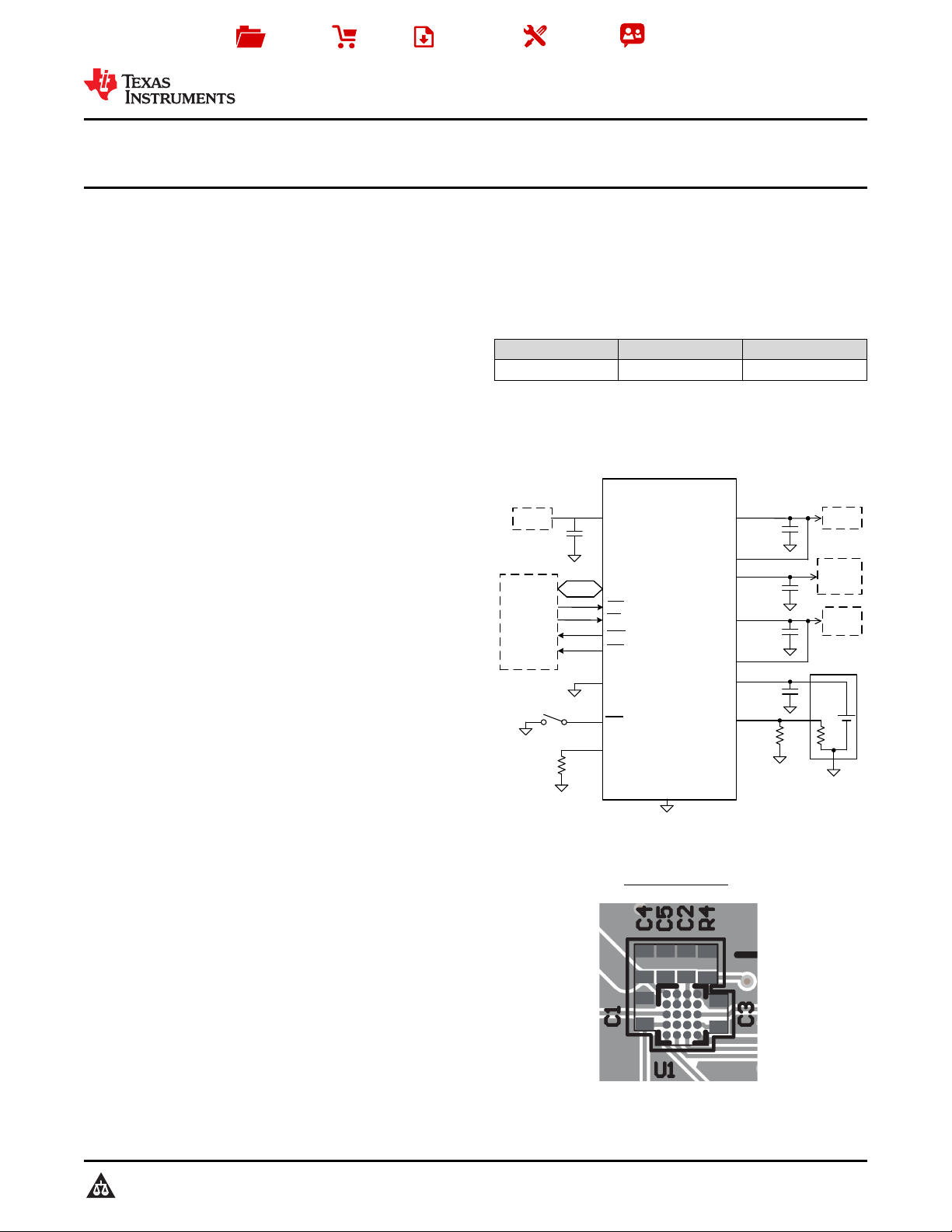
12 mm2 Solution Size
x 0402 Component footprint with 0.2mm pitch
x Pull up and TS resistors not included
BQ25150
VINLS
PMID
LS/LDO
VDD
BAT
TS
+
±
NTC
GND
IN
IMAX
VIO
Host
USB
I2C Bus
<150mA
Load
<10mA
Load
System
ADCIN
MR
PG
INT
LP
CE
C
4
C
5
C
3
C
2
R
4
C
1
Product
Folder
Order
Now
Technical
Documents
Tools &
Software
Support &
Community
BQ25150
SLUSD04B –JULY 2018–REVISED FEBRUARY 2019
BQ25150 500-mA Linear charger with 10-nA ship mode, advanced power path
management and control, ADC, and LDO
1 Features
1
• Linear battery charger with 1.25-mA to 500-mA
• Power path management for powering system and
• I2C Configurable load switch or up to 150-mA
• Ultra low Iddq for extended battery life
• One push-button wake-up and reset input with
• 12-Bit effective ADC
• Always on 1.8-V VDD LDO supporting loads up to
• 20-Pin 2-mm x 1.6-mm CSP package
• 12-mm2Total solution size
2 Applications
• Headsets, earbuds and hearing aids
• Smart watches and fitness accessories
• Patient monitors and portable medical equipment
1
fast charge current range
– 0.5% Accurate I2C programmable battery
regulation voltage ranging from 3.6 V to 4.6 V
in 10-mV steps
– Configurable termination current supporting
down to 0.5 mA
– 20-V Tolerant input with typical 3.4-V to 5.5-V
input voltage operating range
– Programmable thermal charging profile, fully
configurable hot, warm, cool and cold
thresholds
charging battery
– Dynamic power path management optimizes
charging from weak adapters
– Advanced I2C control allows host to disconnect
the battery or adapter as needed
LDO output
– Programmable range from 0.6 V to 3.7 V in
100-mV steps
– 10-nA Ship mode battery Iq
– 400-nA Iq While powering the system (PMID
and VDD on)
adjustable timers
– Supports system power cycle and HW reset
– Monitoring of charge current, battery thermistor
and battery, input and system (PMID) voltages
– General purpose ADC input
10 mA
3 Description
The BQ25150 is a highly integrated battery charge
management IC that integrates the most common
functions for wearable devices, namely a charger, an
output voltage rail, ADC for battery and system
monitoring, and push-button controller.
Device Information
PART NUMBER PACKAGE BODY SIZE (NOM)
BQ25150 DSBGA (20) 2.00 mm x 1.60 mm
(1) For all available packages, see the orderable addendum at
the end of the data sheet.
Simplified Schematic
Solution Area
(1)
An IMPORTANT NOTICE at the end of this data sheet addresses availability, warranty, changes, use in safety-critical applications,
intellectual property matters and other important disclaimers. PRODUCTION DATA.

BQ25150
SLUSD04B –JULY 2018–REVISED FEBRUARY 2019
www.ti.com
Table of Contents
1 Features.................................................................. 1
2 Applications ........................................................... 1
3 Description ............................................................. 1
4 Revision History..................................................... 2
5 Description (continued)......................................... 3
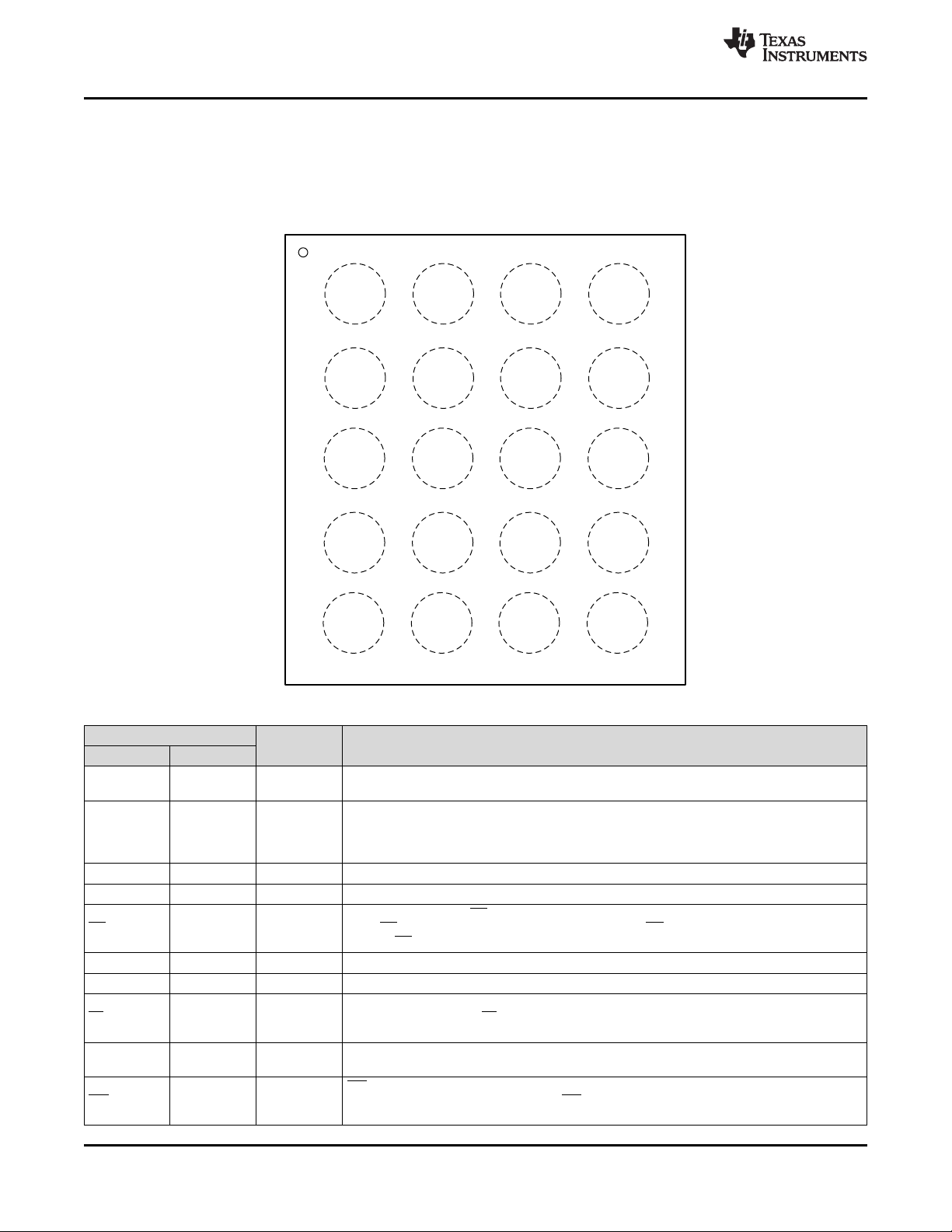
6 Pin Configuration and Functions......................... 4
7 Specifications......................................................... 5
7.1 Absolute Maximum Ratings ...................................... 5
7.2 ESD Ratings.............................................................. 5
7.3 Recommended Operating Conditions....................... 6
7.4 Thermal Information.................................................. 6
7.5 Electrical Characteristics........................................... 6
7.6 Timing Requirements................................................ 9
7.7 Typical Characteristics............................................ 11
8 Detailed Description............................................ 13
8.1 Overview ................................................................. 13
8.2 Functional Block Diagram....................................... 13
8.3 Feature Description................................................. 14
8.4 Device Functional Modes........................................ 33
8.5 Register Map .......................................................... 37
9 Application and Implementation ........................ 92
9.1 Application Information............................................ 92
9.2 Typical Application ................................................. 92
10 Power Supply Recommendations ..................... 98
11 Layout................................................................... 99
11.1 Layout Guidelines ................................................. 99
11.2 Layout Example .................................................... 99
12 Device and Documentation Support............... 100
12.1 Documentation Support ..................................... 100
12.2 Receiving Notification of Documentation
Updates.................................................................. 100
12.3 Community Resources........................................ 100
12.4 Trademarks......................................................... 100
12.5 Electrostatic Discharge Caution.......................... 100
12.6 Glossary.............................................................. 100
13 Mechanical, Packaging, and Orderable
Information......................................................... 100
4 Revision History
NOTE: Page numbers for previous revisions may differ from page numbers in the current version.
Changes from Revision A (October 2018) to Revision B Page
• Deleted 12-Bit from title ......................................................................................................................................................... 1
• Changed from Restricted to Public......................................................................................................................................... 1
• Changed ADC reported resolution TYP value from 12 to 16 ................................................................................................ 8
• Changed T
SHUTDOWN
TYP value from 115°C to 125°C .......................................................................................................... 9
• Changed PUSHBUTTON TIMERS (/MR) number of decimal points in MIN/MAX from 3 to 2 .............................................. 9
• Deleted t
• Deleted t
parameter.................................................................................................................................................... 10
DGL_SC
LP_ENTRY
parameter ................................................................................................................................................ 10
• Changed default state description for watchdog in Safety Timer and I2C Watchdog Timer ............................................... 18
• Deleted 12-Bit from ADC ..................................................................................................................................................... 20
• Changed LS/LDO1 to V
in Load Switch / LDO Output and Control ............................................................................. 21
LSLDO
• Added Section 14-second Watchdog for HW Reset ........................................................................................................... 26
• Changed THERM_REG_2:0 reset value in CHARGERCTRL1 Register (Address = 0x18) [reset = 0x42] section............. 56
• Changed 1_ADCALARM_ABOVE in Table 51..................................................................................................................... 80
• Changed 2_ADCALARM_ABOVE in Table 53 .................................................................................................................... 82
• Changed 3_ADCALARM_ABOVE in Table 55 .................................................................................................................... 84
Changes from Original (July 2018) to Revision A Page
• Changed from Advance Information to Production Data ....................................................................................................... 1
2
Submit Documentation Feedback Copyright © 2018–2019, Texas Instruments Incorporated
Product Folder Links: BQ25150

BQ25150
www.ti.com
SLUSD04B –JULY 2018–REVISED FEBRUARY 2019
5 Description (continued)
The BQ25150 IC integrates a linear charger that enables quick and accurate charging for small batteries. The
device supports charge current up to 500mA and supports termination current down to 0.5mA for maximum
charge. The battery is charged using a standard Li-Ion charge profile with three phases: pre-charge, constant
current and constant voltage regulation.
The device integrates advanced power path management and control that allows the device to provide power to
the system while charging the battery even with poor adapters. The host may also control the power path
through I2C allowing it to disconnect the input adapter and/or battery without physically removing them. The
single push-button input eliminates the need of a separate button controller IC reducing the total solution
footprint. The push-button input can be used for wake functions or to reset the system. A 12-bit effective ADC
enables accurate battery voltage monitoring and can be used to enable a low Iq gauging to monitor battery
health. It can also be used to measure the battery temperature using a thermistor connected to the TS pin as
well as external system signals through a pin. The low quiescent current during operation and shutdown enables
maximum battery life. The input current limit, charge current, LDO output voltage, and other parameters are
programmable through the I2C interface making the BQ25150 a very flexible charging solution. A voltage-based
JEITA compatible (or standard HOT/COLD) battery pack thermistor monitoring input (TS) is included that
monitors battery temperature and automatically changes charge parameters to prevent the battery from charging
outside of its safe temperature range. The temperature thresholds are also programable through I2C allowing the
host to customize the thermal charging profile. The charger is optimized for 5V USB input, with 20V absolute
maximum tolerance to withstand line transients. The device also integrates a linear regulator to provide a quiet
rail for radios or processors and can be independently sourced and controlled through I2C.
Product Folder Links: BQ25150
Submit Documentation FeedbackCopyright © 2018–2019, Texas Instruments Incorporated
3
IN PMID BAT GND
/PG PMID BAT TS
/MR /CE IMAX ADCIN
VDD /INT /LP LSLDO
VIO SDA SCL VINLS
A
B
C
D
E
1 2 3 4
BQ25150
SLUSD04B –JULY 2018–REVISED FEBRUARY 2019
6 Pin Configuration and Functions
www.ti.com
YFP Package
20-Pin DSBGA
Top View
Pin Functions
PIN
NAME NO.
IN A1 I
PMID A2, B2 I/O
GND A4 PWR Ground connection. Connect to the ground plane of the circuit.
VDD D1 O Digital supply LDO. Connect at least 4.7 uF capacitor to ground.
CE C2 I
SCL E3 I/O I2C Interface Clock. Connect SCL to the logic rail through a 10-kΩ resistor.
SDA E2 I I2C Interface Data. Connect SDA to the logic rail through a 10-kΩ resistor.
LP D3 I
IMAX C3 I
INT D2 O
4
Submit Documentation Feedback Copyright © 2018–2019, Texas Instruments Incorporated
I/O DESCRIPTION
DC Input Power Supply. IN is connected to the external DC supply. Bypass IN to GND with
at least 1 uF of capacitance using a ceramic capacitor.
High Side Bypass Connection. Connect at least 10 uF ceramic capacitor (at least 3 uF of
ceramic capacitance with DC bias de-rating) from PMID to GND as close to the PMID and
GND pins as possible. Note: Shorting PMID to IN pin is not recommended as it may cause
large discharge current from battery to IN if IN pin is not truly floating.
Charge Enable. Drive CE low or leave disconnected to enable charging when VIN is valid.
Drive CE high to disable charge when VIN is present. CE is pulled low internally with 900-kΩ
resistor. CE has no effect when VIN is not present.
Low Power Mode Enable. Drive this pin low to enable the device in low power mode when
powered by the battery. LP is pulled low internally with 900 kOhm resistor. This pin has no
effect when VIN is present.
Connect a 10-kOhms or lower resistor to this pin to set the maximum allowable fast charge
current. Must not be left floating.
INT is an open-drain output that signals fault interrupts. When a fault occurs, a 128us pulse
is sent out as an interrupt for the host. INT is enabled/disabled using the MASK_INT bit in
the control register.
Product Folder Links: BQ25150
www.ti.com
SLUSD04B –JULY 2018–REVISED FEBRUARY 2019
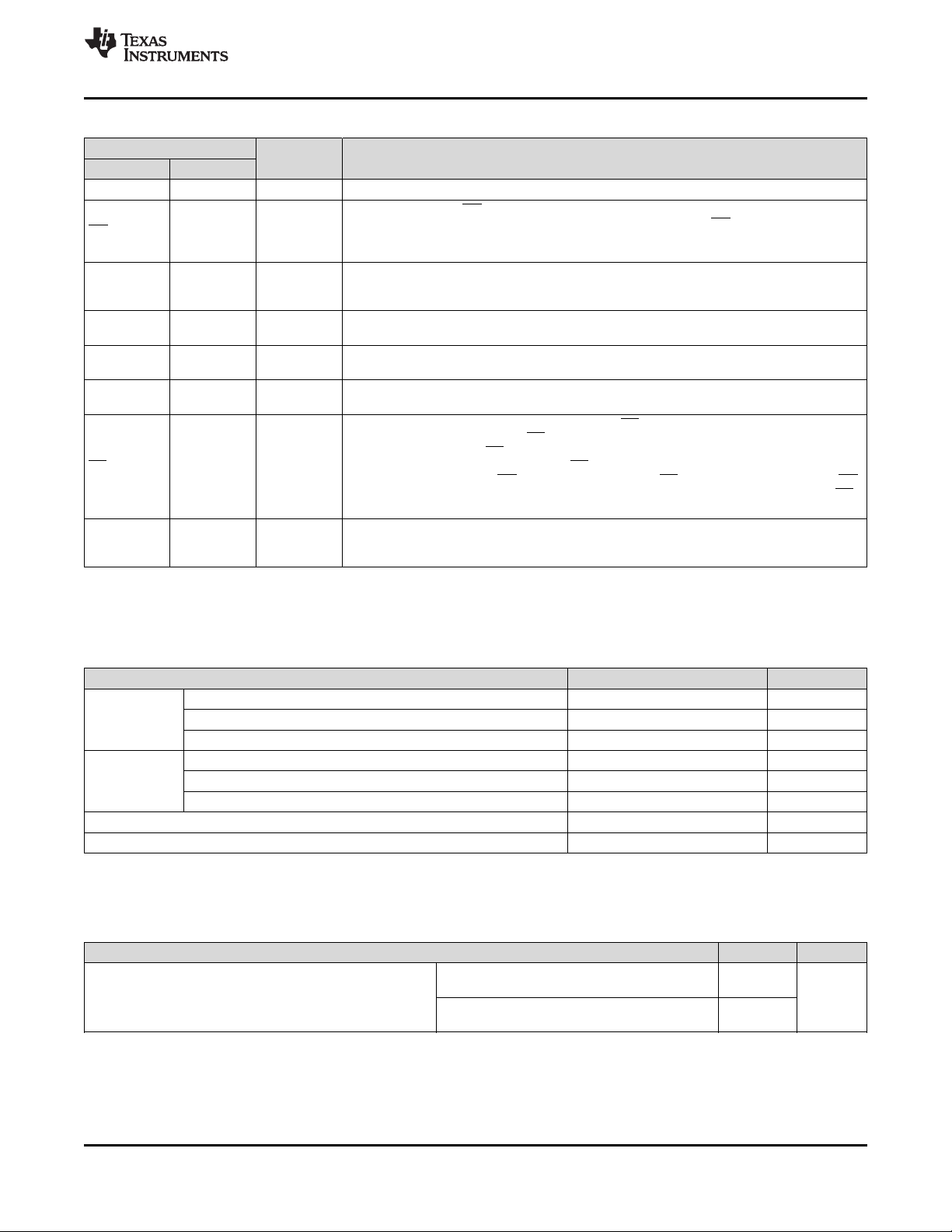
Pin Functions (continued)
PIN
NAME NO.
ADCIN C4 I Input Channel to the ADC. Maximum ADC range 1.2 V.
MR C1 I
LS/LDO D4 O
VINLS E4 I
BAT A3, B3 I/O
TS B4 I
PG B1 O
VIO E1 I
I/O DESCRIPTION
Manual Reset Input. MR is a general purpose input that must be held low for greater than
t
HWRESET
up the device out of Ship Mode when pressed for at least t
to go into HW Reset and power cycle the output rails. If MR is also used to wake
pull-up resistor to BAT.
Load Switch or LDO output. Connect 2.2 uF of ceramic capacitance to this pin to assure
stability. Be sure to account for capacitance bias voltage derating when selecting the
capacitor.
Input to the Load Switch / LDO output. Connect at least 1 uF of ceramic capacitance from
this pin to ground.
Battery Connection. Connect to the positive terminal of the battery. Bypass BAT to GND with
at least 1 uF of ceramic capacitance.
Battery Pack NTC Monitor. Connect TS to a 10kΩ NTC Thermistor in parallel to a 10-kΩ
resistor. If TS function is not to be used connect a 5-kΩ resistor from TS to ground.
Open-drain Power Good status indication output. PG is pulled to GND when VIN is above
V
+ V
BAT
specified limits. Connect PG to the desired logic voltage rail using a 1-kΩ to 100-kΩ resistor,
and less than V
SLP
. PG is high-impedance when the input power is not within
OVP
or use with an LED for visual indication. PG can also be configured through I2C as a pushbutton level shifted output (MR), where the output of the PG pin reflects the status of the MR
input, but pulled up to the desired logic voltage rail using a 1-kΩ to 100-kΩ resistor. The PG
pin can also be configured as a general purpose open drain output.
System IO supply. Connect to system IO supply to allow level shifting of input signals (SDA,
SCL, LP and CE) to the device internal digital domain. Connect to VDD when external IO
supply is not available.
. MR has in internal 125-kΩ
WAKE2
BQ25150
7 Specifications
7.1 Absolute Maximum Ratings
over operating free-air temperature range (unless otherwise noted)
IN –0.3 20 V
Voltage
TS, ADCIN, IMAX, VDD –0.3 1.95 V
All other pins –0.3 5.5 V
IN 0 800 mA
Current
BAT, PMID –0.5 1.5 A
INT, ADCIN, PG 0 10 mA
Junction temperature, T
Storage temperature, T
J
stg
(1) Stresses beyond those listed under Absolute Maximum Rating may cause permanent damage to the device. These are stress ratings
only, which do not imply functional operation of the device at these or any other conditions beyond those indicated under Recommended
Operating Condition. Exposure to absolute-maximum-rated conditions for extended periods may affect device reliability.
7.2 ESD Ratings
Human body model (HBM), per
V
(ESD)
Electrostatic discharge
(1) JEDEC document JEP155 states that 500-V HBM allows safe manufacturing with a standard ESD control process.
(2) JEDEC document JEP157 states that 250-V CDM allows safe manufacturing with a standard ESD control process.
ANSI/ESDA/JEDEC JS-001, all pins
Charged device model (CDM), per JEDEC
specification JESD22-C101, all pins
(1)
MIN MAX UNIT
–40 125 °C
–55 150 °C
VALUE UNIT
(1)
±2000
V
(2)
±500
Product Folder Links: BQ25150
Submit Documentation FeedbackCopyright © 2018–2019, Texas Instruments Incorporated
5
BQ25150
SLUSD04B –JULY 2018–REVISED FEBRUARY 2019
www.ti.com
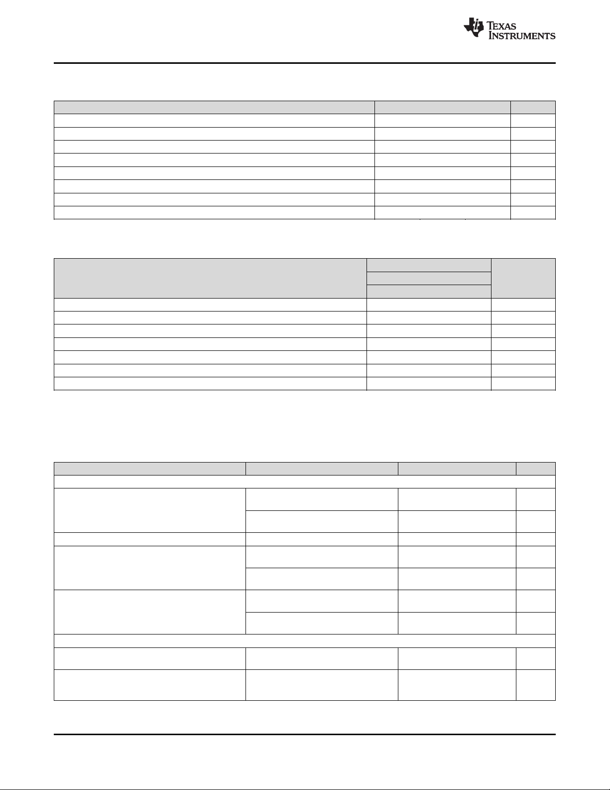
7.3 Recommended Operating Conditions
over operating free-air temperature range (unless otherwise noted)
MIN NOM MAX UNIT
V
BAT
V
IN
V
INLS
V
IO
V
ADCIN
I
LDO
I
PMID
T
A
(1) Based on minimum V
Battery voltage range 2.4 4.6 V
Input voltage range 3.15 5.25
LDO input voltage range 2.2 5.25
(1)
(1)
V
V
IO supply voltage range 1.2 3.6 V
ADC input voltage range 0 1.2 V
LDO output current 0 100 mA
PMID output current 0 500 mA
Operating free-air temperature range –40 85 °C
value. 5.5V under typical conditions
OVP
7.4 Thermal Information
DEVICE
THERMAL METRIC
R
θJA
R
θJA
R
θJC(top)
R
θJB
Ψ
JT
Ψ
JB
R
θJC(bot)
Junction-to-ambient thermal resistance
Junction-to-ambient thermal resistance 74.4 °C/W
Junction-to-case (top) thermal resistance 0.5 °C/W
Junction-to-board thermal resistance 17.6 °C/W
Junction-to-top characterization parameter 0.3 °C/W
Junction-to-board characterization parameter 17.7 °C/W
Junction-to-case (bottom) thermal resistance N/A °C/W
(1) For more information about traditional and new thermal metrics, see the Semiconductor and IC Package Thermal Metrics application
report.
(2) Measured in BQ25150EVM board
(1)
UNITYFP (DSBGA)
20-PIN
(2)
36.1 °C/W
7.5 Electrical Characteristics
VIN= 5V, V
INPUT CURRENTS
I
IN
I
BAT_SHIP
I
BAT_LP
I
BAT_ACTI
VE
POWER PATH MANAGEMENT AND INPUT CURRENT LIMIT
R
ON(IN-
PMID)
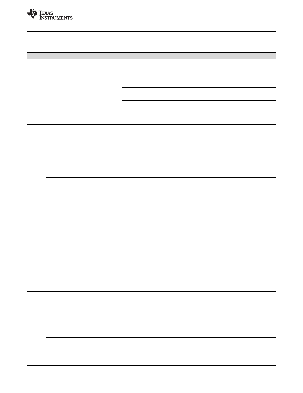
V
BSUP1
= 3.6V. -40°C < TJ< 125°C unless otherwise noted. Typical data at TJ= 25°C
BAT
PARAMETER TEST CONDITIONS MIN TYP MAX UNIT
PMID_MODE= 01, VIN= 5V, V
Input supply current
3.6V
0°C <TJ< 85°C , VIN= 5V, V
Charge Disabled
Battery Discharge Current in Ship Mode 0°C <TJ< 60°C ,VIN= 0V , V
0°C <TJ< 60°C ,VIN= 0V , V
Battery Quiescent Current in Low-power
Mode
LDO Disabled
0°C <TJ< 60°C ,VIN= 0V , V
LDO Enabled
0°C <TJ< 85°C ,VIN= 0V , V
Battery Quiescent Current in Active
Mode
LDO Disabled
0°C <TJ< 85°C ,VIN= 0V , V
LDO Enabled
I
= 500mA (ILIM = 110), VIN= 5V, I
Input FET ON resistance
Enter supplements mode threshold V
ILIM
= 150mA
BAT
> V
BATUVLO
=
BAT
= 3.6V
BAT
= 3.6V 10 150 nA
BAT
= 3.6V,
BAT
= 3.6V,
BAT
= 3.6V,
BAT
= 3.6V,
BAT
IN
,
0.78 1.5 mA
0.46 1.2 µA
1.7 3.5 µA
18 25 µA
21 27 µA
280 520 mΩ
V
<
PMID
V
–
BAT
40mV
500 µA
mV
6
Submit Documentation Feedback Copyright © 2018–2019, Texas Instruments Incorporated
Product Folder Links: BQ25150
www.ti.com
Electrical Characteristics (continued)
BQ25150
SLUSD04B –JULY 2018–REVISED FEBRUARY 2019
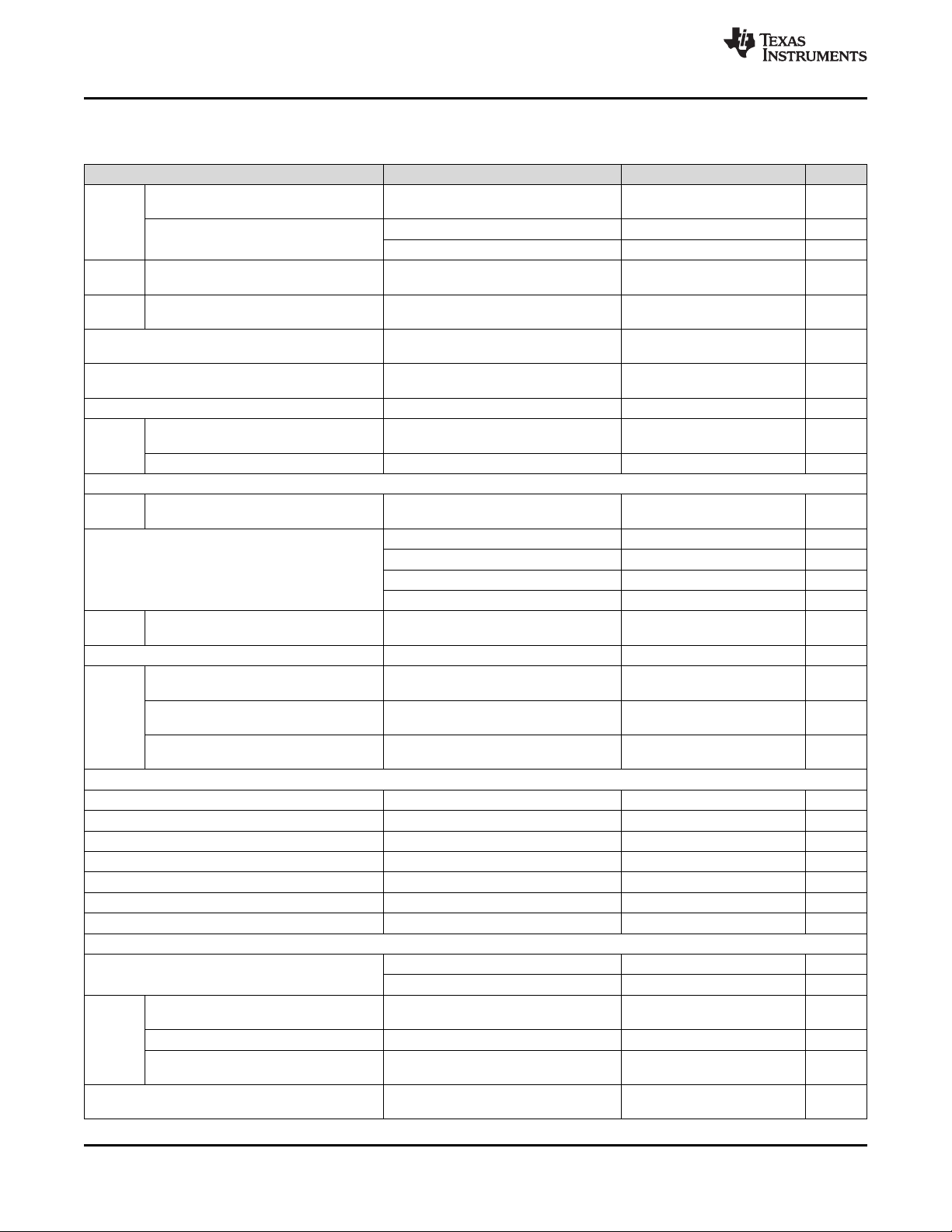
VIN= 5V, V
V
BSUP2
I
ILIM
= 3.6V. -40°C < TJ< 125°C unless otherwise noted. Typical data at TJ= 25°C
BAT
Exit supplements mode threshold V
Input Current Limit
Input DPM voltage threshold where
V
IN_DPM
current in reduced
Accuracy –3 3 %
BATTERY CHARGER
V
DPPM
R
ON(BAT-
PMID)
V
BATREG
PMID voltage threshold when charge
current is reduced
Battery Discharge FET On Resistance V
Charge Voltage Programmable charge voltage range 3.6 4.6 V
Voltage Regulation Accuracy TJ= 25°C 0.5 0.5 %
Fast Charge Programmable Current
I
CHARGE
Range
Fast Charge Current Accuracy TJ= 25°C, I
I
PRECHAR
GE
Precharge current Precharge current programmable range 1.25 77.5 mA
Precharge Current Accuracy -40°C < TJ< 85°C –10 10 %
Termination Charge Current
I
TERM
Accuracy
V
LOWV
V
SHORT
I
SHORT
Programmable voltage threshold for precharge to fast charge transitions
Battery voltage threshold for short
detection
Charge Current in Battery Short
Condition
Recharge Threshold voltage
V
RCH
R
PMID_PD
PMID pull-down resistance V
VDD
V
DD
I
LOAD_VD
D
VDD LDO output voltage
Maximum VDD External load capability V
LS/LDO
Input voltage range for Load switch
Mode
V
INLS
Input voltage range for LDO Mode
PARAMETER TEST CONDITIONS MIN TYP MAX UNIT
V
<
BAT
> V
BATUVLO
PMID
V
BAT
20mV
–
mV
Programmable Range 50 600 mA
I
= 50mA 45 50 mA
ILIM
I
= 100mA 90 100 mA
ILIM
I
= 150mA 135 150 mA
ILIM
I
= 500mA 450 500 mA
ILIM
Programmable Range 4.2 4.9 V
V
- V
PMID
BAT
V
BAT
LOWV
= 4.35V, I
< V
BAT
= 100mA 100 175 mΩ
BAT
< V
BATREG
> 5mA –5 5 %
CHARGE
Termination Current Programmable
Range
TJ= 25°C, I
= 100mA
-10°C < TJ< 85°C, I
I
= 100mA
CHARGE
TERM
= 10% I
TERM
CHARGE
= 10% I
, I
CHARGE
CHARGE
1.25 500 mA
1 31 %
(1)
–5
,
–10
(1)
200 mV
(1)
5
10
%
(1)
%
VBAT rising. Programmable Range 2.8 3 V
VBAT falling, VIN = 5V 2.41 2.54 2.67 V
I
V
< V
BAT
SHORT
V
falling, V
BAT
140mV setting
V
falling, V
BAT
200mV setting
= 3.6V 25 Ω
PMID
V
= 3.6V, VIN= 0V, 0 < I
BAT
10mA
> 3V 10 mA
PMID
BATREG
BATREG
= 4.2V, V
= 4.2V, V
LOAD_VDD
RCH
RCH
=
=
<
PRECHAR
GE
140 mV
200 mV
1.8 V
mA
0.8 5.5 V
2.2 or
V
LDO
500mV
+
5.5 V
(1) Based on Characterization Data
Product Folder Links: BQ25150
Submit Documentation FeedbackCopyright © 2018–2019, Texas Instruments Incorporated
7
BQ25150
SLUSD04B –JULY 2018–REVISED FEBRUARY 2019
Electrical Characteristics (continued)
www.ti.com
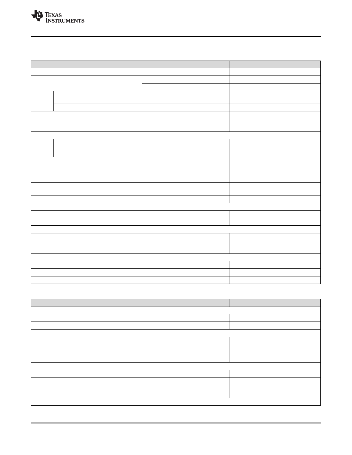
VIN= 5V, V
= 3.6V. -40°C < TJ< 125°C unless otherwise noted. Typical data at TJ= 25°C
BAT
PARAMETER TEST CONDITIONS MIN TYP MAX UNIT
LDO propgrammable output voltage
rnage
V
LDO
LDO output accuracy
ΔV
/ΔI
OUT
OUT
ΔV
V
IN
R
DOSN_L
DO
R
DSCH_LS
LDO
I
OCL_LDO
DC Load Regulation
/Δ
OUT
DC Line Regulation
Switch On resistance V
Discharge FET On-resistance for LS V
Output Current Limit V
LDO VINLS quiescent current in LDO
I
IN_LDO
mode
OFF State Supply Current V
ADC
Resolutio
n
t
ADC_CON
V
Resolutio
n
Bits reported by ADC 16 Bits
Conversion-time
Effective Resolution ADC_SPEED = 00 12 Bits
ADC TS Accuracy
Accuracy
ADC ADCIN Accuracy
ADC VBAT Accuracy
BATTERY PACK NTC MONITOR
V
HOT
V
WARM
V
COOL
V
COLD
V
OPEN
V
HYS
I
TS_BIAS
High temperature threshold VTSfalling, -10°C < TJ< 85°C 0.182
Warm temperature threshold VTSfalling, -10°C < TJ< 85°C 0.262
Cool temperature threshold VTSrising, -10°C < TJ< 85°C 0.510
Cold temperature threshold VTSrising, -10°C < TJ< 85°C 0.581
TS Open threshold VTSrising, -10°C < TJ< 85°C 0.9 V
Threshold hysteresis 4.7 mV
TS bias current -10°C < TJ< 85°C 78.4 80 81.6 µA
PROTECTION
V
UVLO
IN active threshold voltage
Battery undervoltage Lockout Threhshold
Voltage
V
BATUVLO
Accuracy –3 3 %
Battery undervoltage Lockout Threhshold
Voltage at Power Up
V
SLP_ENT
RY
Sleep Entry Threshold (VIN- V
TJ= 25°C –2 2 %
V
0°C < TJ< 85°C, 1 mA < I
V
0°C < TJ< 85°C, Over V
= 100mA, V
V
ADC_SPEED = 00 24 ms
ADC_SPEED = 01 12 ms
ADC_SPEED = 10 6 ms
ADC_SPEED = 11 3 ms
ADC_SPEED = 10 10 Bits
ADC_SPEED = 00, VTS= 0.4V, -10°C <
TJ< 85°C
ADC_SPEED = 00, V
< TJ< 85°C
ADC_SPEED = 00, V
TJ< 85°C
VINrising 3.4 V
VINfalling 3.25 V
Programmable range, 150 mV
Hysteresis
V
) 2.0V < V
BAT
0.6 3.7 V
= 1.8V, V
LDO
= 1.8V
LDO
= 3.6V 250 450 mΩ
INLS
= 3.6V 40 Ω
INLS
= 0V 200 300 mA
LS/LDO
= V
BAT
INLS
= V
BAT
INLS
LDO
INLS
= 1.8V
=3.6V. I
= 1mA –3 3 %
LOAD
< 150mA,
INLS
OUT
range, I
OUT
1.2 %
0.5 %
=3.6V 0.9 µA
=3.6V 0.25 µA
(1)
–1
. 1
= 0.4V, -10°C
ADCIN
= 4.2V, -10°C <
BAT
(1)
–1
1
–0.4 0.4 %
(1)
0.185 0.189
(1)
0.265 0.268
(1)
0.514 0.518
(1)
0.585 0.589
2.4 3 V
rising, VIN= 0V, TJ= 25°C 3.15 V
BAT
BAT
< V
, VINfalling 80 mV
BATREG
(1)
%
(1)
%
(1)
V
(1)
V
(1)
V
(1)
V
8
Submit Documentation Feedback Copyright © 2018–2019, Texas Instruments Incorporated
Product Folder Links: BQ25150
www.ti.com
Electrical Characteristics (continued)
BQ25150
SLUSD04B –JULY 2018–REVISED FEBRUARY 2019
VIN= 5V, V
= 3.6V. -40°C < TJ< 125°C unless otherwise noted. Typical data at TJ= 25°C
BAT
PARAMETER TEST CONDITIONS MIN TYP MAX UNIT
V
SLP_EXIT
V
OVP
Sleep Exit Threshold (VIN- V
Input Supply Over Voltage Threshold
Batery Over Current Threshold
I
BAT_OCP
Programmable range
Current Limit Accuracy –30 30 %
T
SHUTDO
WN
T
HYS
Thermal shutdown trip point 125 °C
Thermal shutdown trip point hysteresis 15 °C
I2C INTERFACE (SCL and SDA)
I2C
Frequen
cy
V
V
V
I
IL
IH
OL
LKG
Input Low threshold level V
Input High Threshold level V
Output Low threshold level V
High-level leakage Current V
/MR INPUT
R
PU
V
IL
Internal pull up resistance 90 125 170 kΩ
/MR Input Low threshold level V
/INT, /PG OUTPUTS
V
I
OL
LKG
Output Low threshold level V
/INT Hi level leakage Current High Impedance, V
/CE, /LP INPUTS
R
PDOWN
V
IL
V
IH
/CE pull down resistance 900 kΩ
Input Low threshold level VIO= 1.8V 0.45 V
/CE Input High Threshold level VIO= 1.8V 1.35 V
) 2.0V < V
BAT
BAT
< V
BATREG
130 mV
VINrising 5.35 5.5 5.8 V
VINfalling (125mV hysteresis) 5.4 V
I
BAT_OCP
increasing 1200 1600 mA
100 400 kHz
= VIO= 1.8V
PULLUP
= VIO= 1.8V
PULLUP
= VIO= 1.8V, I
PULLUP
= VIO= 1.8V 1 µA
PULLUP
> V
BAT
BUVLO
= VIO= 1.8V, I
PULLUP
PULLUP
= 5mA
LOAD
= 5mA
LOAD
= VIO= 1.8V 1 µA
0.75 *
V
IO
0.25 *
V
IO
0.25 *
V
IO
0.3 V
0.25 *
V
IO
V
V
V
V
7.6 Timing Requirements
PARAMETER TEST CONDITIONS MIN TYP MAX UNIT
BATTERY CHARGE TIMERS
t
MAXCHG
t
PRECHG
WATCHDOG TIMERS
t
WATCHDO
G_SW
t
HW_RESE
T_WD
LDO
t
ON_LDO
t
OFF_LDO
t
PMID_LDO
_DELAY
PUSHBUTTON TIMERS (/MR)
Charge safety timer Programmable range 180 720 min
Precharge safety timer 0.25 * t
SW Watchdog timer 25 50 s
HW reset watchdog timer WATCHDOG_15S_ENABLE = 1 15 s
Turn ON time 100mA load, to 90% V
Turn OFF time 100mA load, to 10% V
Delay between PMID and LDO enable
during power up
MAXCHG
LDO
LDO
500 µs
30 µs
Startup 20 ms
Submit Documentation FeedbackCopyright © 2018–2019, Texas Instruments Incorporated
Product Folder Links: BQ25150
9

BQ25150
SLUSD04B –JULY 2018–REVISED FEBRUARY 2019
Timing Requirements (continued)
PARAMETER TEST CONDITIONS MIN TYP MAX UNIT
t
WAKE1
t
WAKE2
t
RESET_W
ARN
t
HW_RESE
T
t
RESTART(
AUTOWAK
E)
PROTECTION
t
DGL_SLP
t
DGL_OVP
t
DGL_OCP
t
REC_SC
t
RETRY_S
C
t
DGL_SHT
DWN
I2C INTERFACE
t
WATCHDO
G
t
I2CRESET
INPUT PINS (/CE and /LP)
t
LP_EXIT_I
2C
WAKE1 Timer. Time from /MR falling
edge to INT being asserted.
WAKE2 Timer. Time from /MR falling
edge to INT being asserted.
RESET_WARN Timer. Time prior to HW
RESET
HW RESET Timer. Time from /MR falling
edge to HW Reset
RESTART Timer. Time from /MR HW
Reset to PMID power up
Deglitch time for supply rising above
V
+ V
SLP
SLP_HYS
Deglitch time for V
Threshold VIN falling below V
OVP
Battery OCP deglitch time 30 µs
Recovery time, BAT Short Circuit during
Discharge Mode
Retry window for PMID or BAT short
circuit recovery
Deglitch time, Thermal shutdown TJrising above T
I2C interface reset timer for host When enabled 50 s
I2C interface inactive reset timer 500 ms
Time for device to exit Low-power mode
and allow I2C communication
www.ti.com
MR_WAKE1_TIMER = 0 106 125 144 ms
MR_WAKE1_TIMER = 1 425 500 575 ms
MR_WAKE2_TIMER = 0 0.85 1 1.15 s
MR_WAKE2_TIMER = 1 1.7 2 2.3 s
MR_RESET_WARN = 00 0.42 0.5 0.58 s
MR_RESET_WARN = 01 0.85 1 1.15 s
MR_RESET_WARN = 10 1.27 1.5 1.73 s
MR_RESET_WARN = 11 1.7 2 2.3 s
MR_HW_RESET = 00 3.4 4 4.6 s
MR_HW_RESET = 01 6.8 8 9.2 s
MR_HW_RESET = 10 8.5 10 11.5 s
MR_HW_RESET = 11 11.9 14 16.1 s
AUTOWAKE = 00 0.52 0.6 0.68 s
AUTOWAKE = 01 1.05 1.2 1.35 s
AUTOWAKE = 10 2.11 2.4 2.69 s
AUTOWAKE = 11 4.4 5 5.6 s
120 µs
OVP
32 ms
250 ms
2 s
SHUTDOWN
10 µs
VIN= 0V. 1 ms
10
Submit Documentation Feedback Copyright © 2018–2019, Texas Instruments Incorporated
Product Folder Links: BQ25150
V
INLS
(V)
R
DSON
(:)
1 1.5 2 2.5 3 3.5 4 4.5 5
0
0.2
0.4
0.6
0.8
1
1.2
D015
TJ = -40C
TJ = 25C
TJ = 85C
I
LOAD
(A)
V
LDO
(V)
0.1 0.11 0.12 0.13 0.14 0.15 0.16 0.17 0.18 0.19 0.2
0.7984
0.7992
0.8
0.8008
0.8016
0.8024
0.8032
0.804
0.8048
0.8056
0.8064
D009
TJ = -40C
TJ = 25C
TJ = 85C
I
PRECHARGE
(A)
Error (%)
0 5 10 15 20 25 30 35 40 45 50 55 60 65 70 75 80
-1.2
-1
-0.8
-0.6
-0.4
-0.2
0
0.2
0.4
0.6
0.8
1
1.2
D013
TJ = 25C
TJ = 0C
TJ = -40C
TJ = 60C
TJ = 125C
I
PRECHARGE
(mA)
Error (%)
0 5 10 15 20 25 30 35 40
-1.5
-1
-0.5
0
0.5
1
1.5
D012
TJ = 25C
TJ = 0C
TJ = -40C
TJ = 60C
TJ = 125C
V
BATREG
(V)
Error (%)
3.6 3.7 3.8 3.9 4 4.1 4.2 4.3 4.4 4.5 4.6
-0.5
-0.45
-0.4
-0.35
-0.3
-0.25
-0.2
-0.15
-0.1
-0.05
0
D011
TJ = 25C
TJ = 0C
TJ = -40C
TJ = 60C
TJ = 125C
I
CHARGE
(A)
Error (%)
0 0.05 0.1 0.15 0.2 0.25 0.3 0.35 0.4 0.45 0.5
-1.75
-1.5
-1.25
-1
-0.75
-0.5
-0.25
0
0.25
0.5
0.75
1
1.25
D014
TJ = -40C
TJ = 0C
TJ = 25C
TJ = 60C
TJ = 125C
www.ti.com
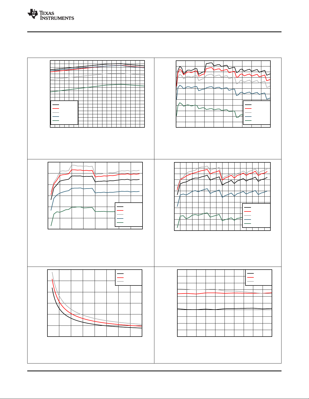
7.7 Typical Characteristics
CIN= 1µF, C
= 10µF, C
PMID
LSLDO
= 2.2µF, C
= 1µF (unless otherwise specified)
BAT
BQ25150
SLUSD04B –JULY 2018–REVISED FEBRUARY 2019
VIN = 5V
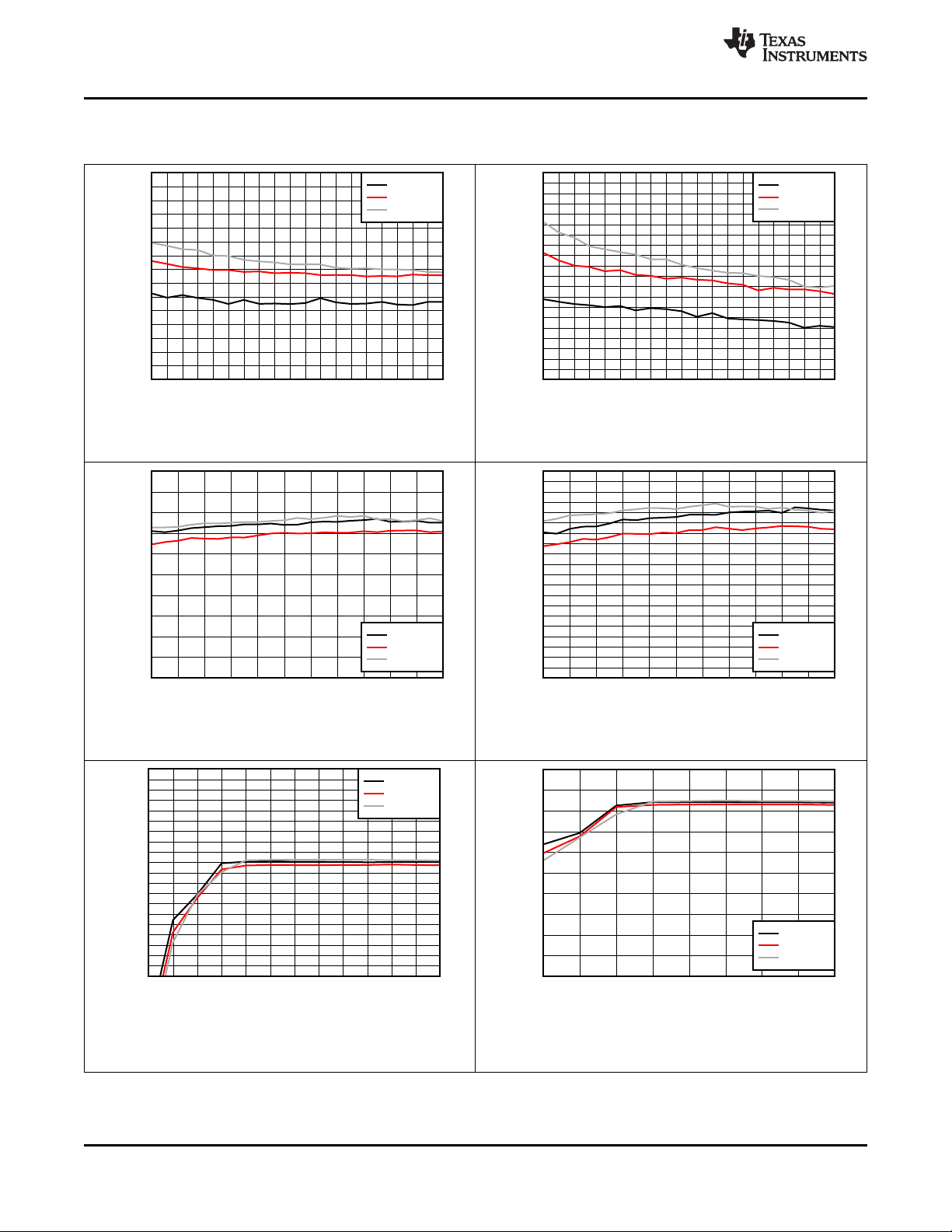
Figure 1. Battery Regulation Voltage Accuracy vs.
VBATREG Setting setting
VIN = 5V VBAT = 2.7V
Figure 3. Pre-Charge Current Accuracy vs. IPRECHARGE
setting (ICHARGE_RANGE = 0)
VIN = 5V VBAT = 3.6 V ICHARGE_RANGE
= 1
Figure 2. Charge Current Accuracy vs. ICHARGE setting
VBUS = 5V VBAT = 2.7V ICHARGE_RANGE
= 1
Figure 4. Pre-Charge Current Accuracy vs. IPRECHARGE
Setting (ICHARGE_RANGE = 1)
VBUS = 5V
Figure 5. LS/LDO Switch On Resistance vs. VINLS
Product Folder Links: BQ25150
VIN = 0V VBAT = 3.6V VINLS = VPMID
Figure 6. LDO Load Regulation (VLDO = 0.8V)
Submit Documentation FeedbackCopyright © 2018–2019, Texas Instruments Incorporated
11
V
INLS
(V)
VLDO (V)
3.2 3.3 3.4 3.5 3.6 3.7 3.8 3.9 4 4.1 4.2 4.3 4.4
3.2
3.22
3.24
3.26
3.28
3.3
3.32
3.34
3.36
3.38
3.4
D006
TJ = -40C
TJ = 25C
TJ = 85C
V
INLS
(V)
V
LDO
(V)
3.6 3.7 3.8 3.9 4 4.1 4.2 4.3 4.4
3.4
3.425
3.45
3.475
3.5
3.525
3.55
3.575
3.6
3.625
3.65
D007
TJ = -40C
TJ = 25C
TJ = 85C
V
INLS
(V)
V
LDO
(V)
2.2 2.4 2.6 2.8 3 3.2 3.4 3.6 3.8 4 4.2 4.4
1.19
1.192
1.194
1.196
1.198
1.2
1.202
1.204
1.206
1.208
1.21
D004
TJ = -40C
TJ = 25C
TJ = 85C
V
INLS
(V)
V
LDO
(V)
2.2 2.4 2.6 2.8 3 3.2 3.4 3.6 3.8 4 4.2 4.4
1.79
1.792
1.794
1.796
1.798
1.8
1.802
1.804
1.806
1.808
1.81
D005
TJ = -40C
TJ = 25C
TJ = 85C
I
LOAD
(A)
V
LDO
(V)
0.01 0.03 0.05 0.07 0.09 0.11 0.13 0.15 0.17 0.19
1.79
1.792
1.794
1.796
1.798
1.8
1.802
1.804
1.806
1.808
1.81
1.812
1.814
1.816
1.818
1.82
D008
TJ = -40C
TJ = 25C
TJ = 85C
I
LOAD
(A)
V
LDO
(V)
0.01 0.03 0.05 0.07 0.09 0.11 0.13 0.15 0.17 0.19
3.29
3.294
3.298
3.302
3.306
3.31
3.314
3.318
3.322
3.326
3.33
D010
TJ = -40C
TJ = 25C
TJ = 85C
BQ25150
SLUSD04B –JULY 2018–REVISED FEBRUARY 2019
Typical Characteristics (continued)
www.ti.com
CIN= 1µF, C
= 10µF, C
PMID
LSLDO
= 2.2µF, C
= 1µF (unless otherwise specified)
BAT
VIN = 0V VBAT = 3.6V VINLS = VPMID
Figure 7. LDO Load Regulation (VLDO = 1.8V)
VIN = 0V VBAT = 3.6V VINLS= VPMID
Figure 8. LDO Load Regulation (VLDO = 3.3V)
VBAT = 4.4V ILOAD = 150mA
Figure 9. LDO Line Regulation (VLDO = 1.2V)
12
VBAT = 4.4V ILOAD = 150mA
Figure 11. LDO Line Regulation (VLDO = 3.3V)
Submit Documentation Feedback Copyright © 2018–2019, Texas Instruments Incorporated
VBAT = 4.4V ILOAD = 150mA
Figure 10. LDO Line Regulation (VLDO = 1.8V)
VBAT = 4.4V ILOAD =
150mA
Figure 12. LDO Line Regulation (VLDO = 3.6V)
Product Folder Links: BQ25150
LDO, and BAT FET Control
Device Control
V
IN
Charge
Enable
I2C
Interface
Low Power Mode
Control
Maximum Charge
Current
Charge Control
LDO / Load Switch
Control
Thermal
Shutdown
I
BATREG
LDO
Control
UVLO
V
BATREG
V
IN_DPM
BAT
VIN
+
±
ADC
/Power Good
GP Output
Interrupt
JEITA/Temp
Battery Voltage
Charge Current
Information
For Charge Control
VDD
VIN
IIN
PMID
VIN
IIN
VPMID
ICHG
VBAT
VTS
Ext.
S
G
D
S
G
D
Q7
Q8
IN
GND
VIO
/CE
SCL
SDA
/LP
IMAX
/MR
/INT
/PG
PMID
VDD
VINLS
LDO
BAT
TS
ADCIN
V
BATUVLO
Q5/Q6
BQ25150
www.ti.com
SLUSD04B –JULY 2018–REVISED FEBRUARY 2019
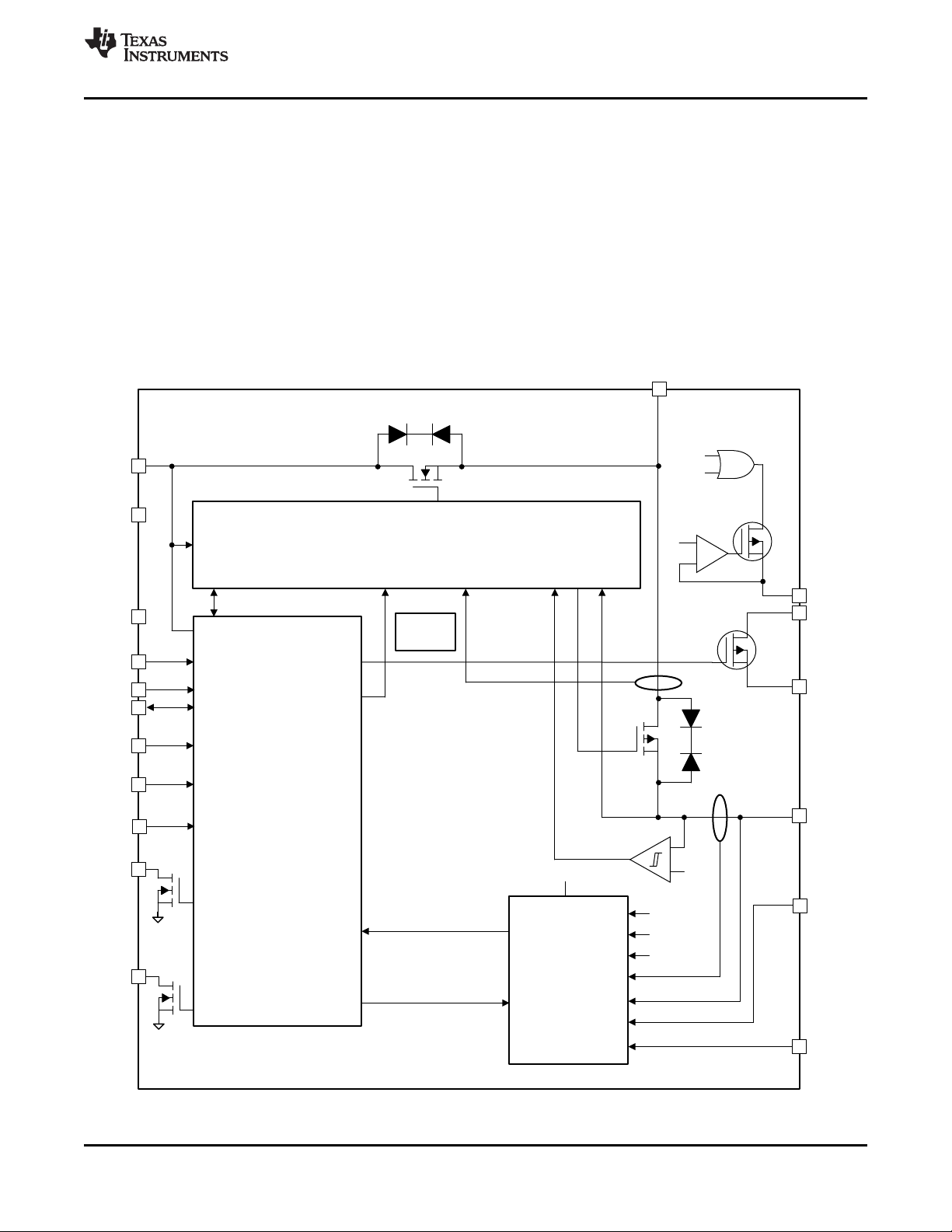
8 Detailed Description
8.1 Overview
The BQ25150 IC is a highly programmable battery management device that integrates a 500mA linear charger
for single cell Li-Ion batteries, a 12-bit effective ADC, a general purpose LDO that may be configured as a load
switch, and a push-button controller. Through it's I2C interface the host may change charging parameters such as
battery regulation voltage and charge current, and obtain detailed device status and fault information. The host
may also read ADC measurements for battery and input voltage among other parameters, including the ADCIN
pin voltage. The push-button controller allows the user to reset the system without any intervention from the host
and wake up the device from Ship Mode.
8.2 Functional Block Diagram
Product Folder Links: BQ25150
Submit Documentation FeedbackCopyright © 2018–2019, Texas Instruments Incorporated
13

BQ25150
SLUSD04B –JULY 2018–REVISED FEBRUARY 2019
www.ti.com
8.3 Feature Description
8.3.1 Linear Charger and Power Path
The BQ25150 IC integrates a linear charger that allows the battery to be charged with a programmable charge
current of up to 500mA. In addition to the charge current, other charging parameters can be programmed through
I2C such as the battery regulation voltage, pre-charge current, termination current, and input current limit current.
The power path allows the system to be powered from PMID, even when the battery is dead or charging, by
drawing power from IN pin. It also prioritizes the system load connected to PMID, reducing the charging current,
if necessary, in order support the load when input power is limited. If the input supply is removed and the battery
voltage level is above V
BATUVLO
There are several control loops that influence the charge current: constant current loop (CC), constant voltage
loop (CV), input current limit, VDPPM, and VINDPM. During the charging process, all loops are enabled and the
one that is dominant takes control regulating the charge current as needed. The charger input has back to back
blocking FETs to prevent reverse current flow from PMID to IN. They also integrate control circuitry regulating the
input current and prevents excessive currents from being drawn from the IN power supply for more reliable
operation.
The device supports multiple battery regulation voltage regulation settings (V
options to support multiple battery chemistries for single-cell applications.
A more detailed description of the charger functionality is presented in the following sections of this document.
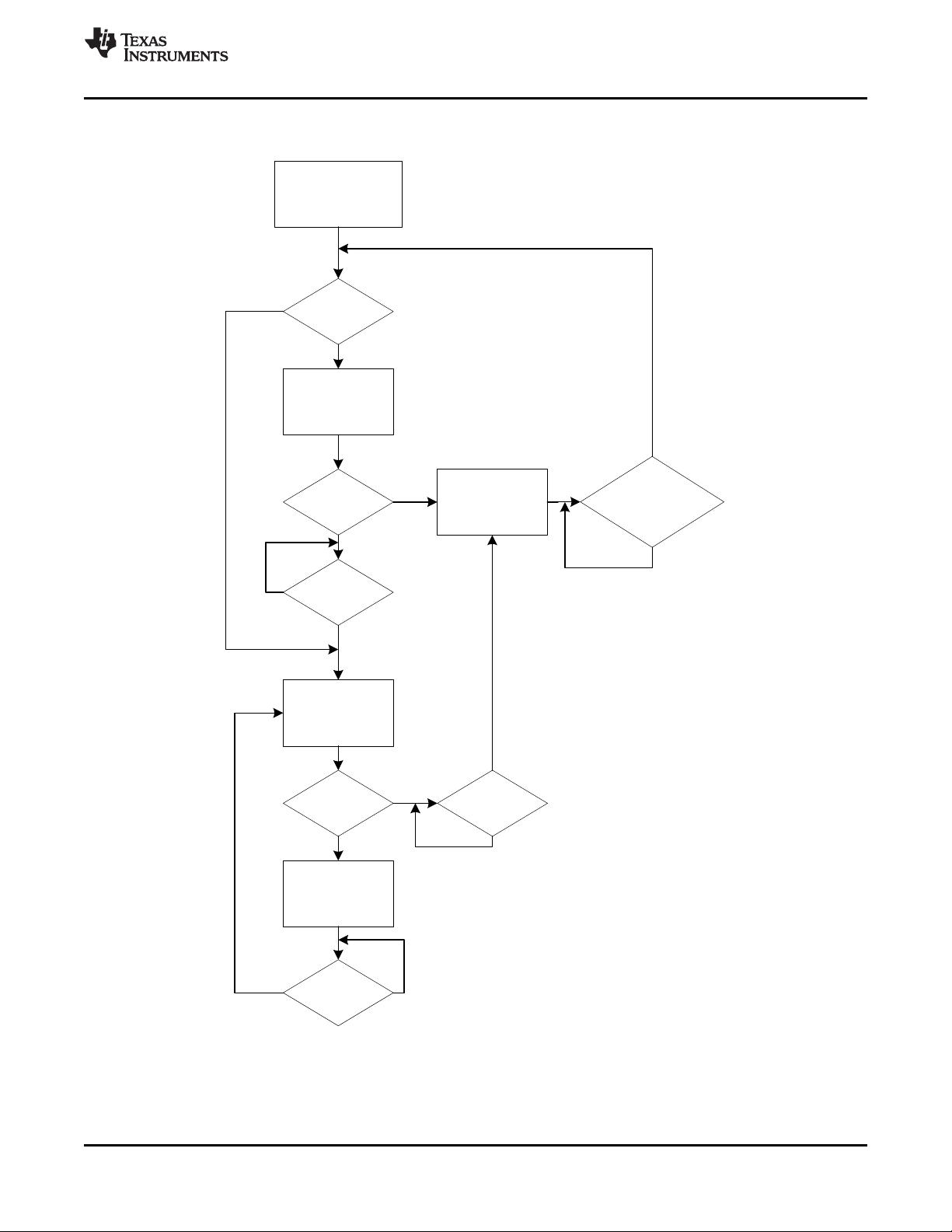
8.3.1.1 Battery Charging Process
The following diagram summarizes the charging process of the BQ25150 charger.
, PMID will automatically and seamlessly switch to battery power.
) and charge current (I
BATREG
CHARGE
)
14
Submit Documentation Feedback Copyright © 2018–2019, Texas Instruments Incorporated
Product Folder Links: BQ25150
V
BAT
< V
LOWV
Start Precharge
Icharge set by I2C
Connect VIN
Precharge safety
timer expired?
Stop Charging and set
Fault bits
/CE toggled or VIN and
removed and
reconnected?
V
BAT
> V
LOWV
Start FastCharge
Icharge set by I2C, max
value limited by IMAX
resistor
I
BAT
< I
TERM
Fast Charge safety
timer expired?
Charge Done (Set bit
and interrupt and
disconnect BATFET)
V
BAT
< V
BAT
- V
RCH
Yes
No
Yes
No
Yes
No
Yes
No
Yes
No
Yes
No
Yes No
www.ti.com
Feature Description (continued)
BQ25150
SLUSD04B –JULY 2018–REVISED FEBRUARY 2019
Figure 13. BQ25150 Charger Flow Diagram
Product Folder Links: BQ25150
Submit Documentation FeedbackCopyright © 2018–2019, Texas Instruments Incorporated
15
BQ25150
SLUSD04B –JULY 2018–REVISED FEBRUARY 2019
Feature Description (continued)
www.ti.com
When a valid input source is connected (VIN> V
UVLO
and V
BAT+VSLP
< VIN< V
), the state of the CE pin
OVP
determines whether a charge cycle is initiated. When the CE input is high and a valid input source is connected,
the battery charge FET is turned off, preventing any kind of charging of the battery. A charge cycle is initiated
when the CHARGE_DISABLE bit is written to 0 and CE pin in low. The following table shows the CE pin and bit
priority to enable/disable charging.
Table 1. Charge Enable Function Through CE Pin and CE Bit
/CE PIN CHARGE _DISABLE BIT CHARGING
0 0 Enabled
0 1 Disabled
1 0 Disabled
1 1 Disabled
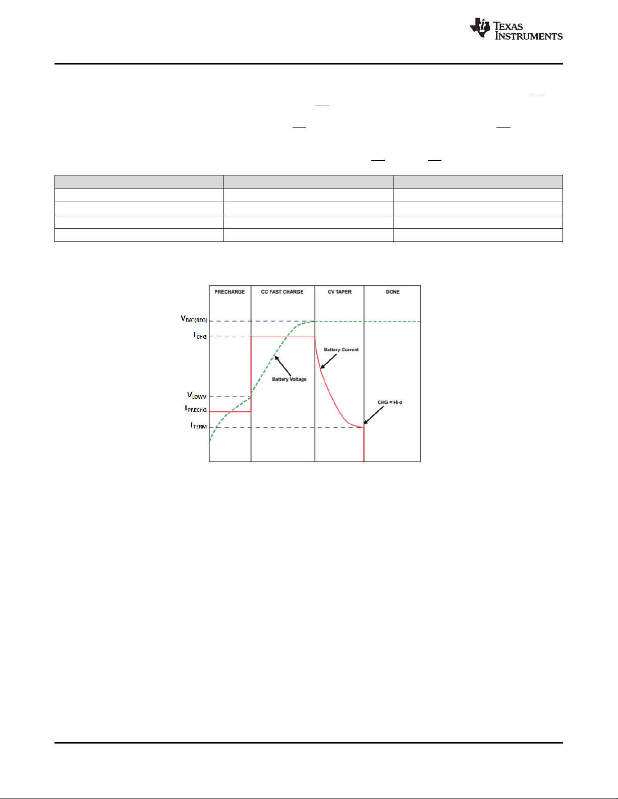
The following figure shows a typical charge cycle.
Figure 14. BQ25150 Typical Charge Cycle
8.3.1.1.1 Pre-Charge
In order to prevent damage to the battery, the device will charge the battery at a much lower current level when
the battery voltage (V
through I2C. Once the battery voltage reaches V
charging the battery at I
) is below the V
BAT
CHARGE
.
level. The pre-charge current (I
LOWV
, the charger will then operate in Fast Charge Mode,
LOWV
PRECHARGE
) can be programmed
During pre-charge, the safety timer is set to 25% of the safety timer value during fast charge.
8.3.1.1.2 Fast Charge
The charger has two main control loops that control charging when V
Constant Voltage (CV) loops. When the CC loop is dominant, typically when V
is charged at the maximum charge current level I
CHARGE
, unless there is a TS fault condition (JEITA operation),
BAT
> V
: the Constant Current (CC) and
LOWV
BAT
< V
BATREG
– 50 mV, the battery
thermal charge current foldback is active, VINDPM is active, or DPPM is active. (See respective sections for
details on these modes of operation). Once the battery voltage approaches the V
BATREG
level, the CV loop
becomes more dominant and the charging current starts tapering off as shown in Figure 14. Once the charging
current reaches the termination current (I
) charging is stopped.
TERM
The maximum fast charge current is limited by the IMAX resistor setting, even if a higher I2C value is
programmed. See Maximum Allowable Charging Current (IMAX) for details on IMAX function.
16
Submit Documentation Feedback Copyright © 2018–2019, Texas Instruments Incorporated
Product Folder Links: BQ25150

BQ25150
www.ti.com
8.3.1.1.3 Pre-Charge to fast Charge Transitions and Charge Current Ramping
SLUSD04B –JULY 2018–REVISED FEBRUARY 2019
Whenever a change in the charge current setting is triggered, whether it occurs due to I2C programming by the
host, Pre-Charge/Fast Charge transition or JEITA TS control, the device will temporarily disable charging (for ~
1ms) before updating the charge current value.
8.3.1.1.4 Termination
The device will automatically terminate charging once the charge current reaches I
, which is programmable
TERM
through I2C.
After termination the charger will operate in high impedance mode, disabling the BATFET to disconnect the
battery. Power is provided to the system (PMID) by IN supply as long and VIN> V
V
.
OVP
UVLO
and V
BAT+VSLP
< VIN<
Termination is only enabled when the charger CV loop is active in fast charge operation. No termination will
occur if the charge current reaches I
while VINDPM or DPPM is active as well as the thermal regulation
TERM
loop. Termination is also disabled when operating in the TS WARM region. The charger only goes to termination
when the current drops to I
due to the battery reaching the target voltage and not due to the charge current
TERM
limitation imposed by the previously mentioned control loops.
8.3.1.2 JEITA and Battery Temperature Dependent Charging
The charger can be configured through I2C setting to provide JEITA support, automatically reducing the charging
current and voltage depending on the battery temperature as monitored by an NTC thermistor connected to the
BQ25150 TS pin. See External NTC Monitoring (TS) for details.
8.3.1.3 Input Voltage Based Dynamic Power Management (VINDPM)
The VINDPM loop prevents the input voltage from collapsing to a point where charging would be interrupted by
reducing the current drawn by charger in order to keep VINfrom dropping below V
IN_DPM
.
During the normal charging process, if the input power source is not able to support the programmed or default
charging current and system load, the voltage at the IN pin decreases. Once the IN voltage drops to V
IN_DPM
, the
VINDPM current and voltage loops will reduce the input current through the blocking FETs, to prevent the further
drop of the supply voltage. The V
threshold is programmable through the I2C register from 4.2 V to 4.9 V in
IN_DPM
100 mV steps. It can be disabled completely as well. When the device enters this mode, the charge current may
be lower than the set value and the V
V
is active. Additionally, termination is disabled.
IN_DPM
INDPM_STAT
bit is set. If the 2X timer is set, the safety timer is extended while
8.3.1.4 Dynamic Power Path Management Mode (DPPM)
With a valid input source connected, the power-path management circuitry monitors the input voltage and current
continuously. The current into IN is shared at PMID between charging the battery and powering the system load
connected at PMID. If the sum of the charging and load currents exceeds the preset maximum input current set
by ILIM, PMID starts to drop. If PMID drops below the DPPM voltage threshold, the charging current is reduced
by the DPPM loop through the BATFET. If PMID continues to drop after BATFET charging current is reduced to
zero, the part will enter supplement mode when PMID falls below the supplement mode threshold (V
V
). Battery termination is disabled while in DPPM mode. The V
BSUP1
V
. This will enable supporting lower input voltages to minimize losses through the linear charger.
BAT
threshold is typically 200 mV above
DPPM
BAT
8.3.1.5 Battery Supplement Mode
While in DPPM mode, if the charging current falls to zero and the system load current increases beyond the
programmed input current limit, the voltage at PMID reduces further. When the PMID voltage drops below the
battery voltage by V
load when the voltage on the PMID pin rises above the battery voltage by V
, the battery supplements the system load. The battery stops supplementing the system
BSUP1
. During supplement mode, the
BSUP2
battery supplement current is not regulated, however, the Battery Over-Current Protection mechanism is active.
Battery charge termination is disabled while in supplement mode.
-
Product Folder Links: BQ25150
Submit Documentation FeedbackCopyright © 2018–2019, Texas Instruments Incorporated
17

( )
BAT PMID BAT BAT
P V V I u
/ / /
( )
LS LDO INLS LS LDO LS LDO
P V V I u
( )
PMID IN PMID IN
P V V I u
/DISS PMID LS LDO BAT
P P P P
BQ25150
SLUSD04B –JULY 2018–REVISED FEBRUARY 2019
www.ti.com
8.3.2 Protection Mechanisms
8.3.2.1 Input Over-Voltage Protection
The input over-voltage protection protects the device and downstream components connected to PMID, and BAT
against damage from over-voltage on the input supply. When VIN> V
an OVP fault is determined to exist.
OVP
During the OVP fault, the device turns the input FET off, sends a single 128 us pulse on INT, and the
VIN_OVP_FAULT FLAG and STAT bits are updated over I2C. Once the OVP fault is removed, the STAT bit is
cleared and the device returns to normal operation. The FLAG bit is not cleared until it is read through I2C after
the OVP condition no longer exists. The OVP threshold for the device is 5.5 V to allow operation from standard
USB sources.
8.3.2.2 Safety Timer and I2C Watchdog Timer
At the beginning of the charge cycle, the device starts the safety timer. If charging has not terminated before the
programmed safety time, t
t
MAXCHG
. When a safety timer fault occurs, a single 128us pulse is sent on the INT pin and the
MAXCHG
, expires, charging is disabled. The pre-charge safety time, t
PRECHG
, is 25% of
SAFETY_TMR_FAULT_FLAG bit in the FLAG3 register is updated over I2C. The CE pin or input power must be
toggled in order to reset the safety timer and exit the fault condition. Note that the flag bit will be reset when the
bit is read by the host even if the fault has not been cleared. The safety timer duration is programmable using the
SAFETY_TIMER bits. When the safety timer is active, changing the safety timer duration resets the safety timer.
The device also contains a 2X_TIMER bit that doubles the timer duration prevent premature safety timer
expiration when the charge current is reduced by a high load on PMID (DPM operation), VIN DPM, thermal
regulation, or a NTC (JEITA) condition. When 2X_TIMER function is enabled, the timer is allowed to run at half
speed when any loop is active other than CC or CV.
In addition to the safety timer, the device contains a 50-second I2C watchdog timer that monitors the host
through the I2C interface. The watchdog timer is enabled by default and may be enabled by the host through I2C.
Once the watchdog timer is enabled, the watchdog timer is started. The watchdog timer is reset by any
transaction by the host using the I2C interface. If the watchdog timer expires without a reset from the I2C
interface, all charger parameters registers (ICHARGE, IPRECHARGE, ITERM,VLOWV, etc) are reset to the
default values.
8.3.2.3 Thermal Protection and Thermal Charge Current Foldback
During operation, to protect the device from damage due to overheating, the junction temperature of the die, TJ,
is monitored. When TJreaches T
operation when TJfalls below T
SHUTDOWN
SHUTDOWN
the device stops operation and is turned off. The device resumes
by T
HYS
.
During the charging process, to prevent overheating in the device, the device monitors the junction temperature
of the die and reduces the charging current at a rate of (0.04 x I
foldback threshold, T
. If the charge current is reduced to 0, the battery supplies the current needed to supply
REG
CHARGE
)/°C once TJexceeds the thermal
the PMID output. The thermal regulation threshold may be set through I2C by setting the THERM_REG bits to
the desired value.
To ensure that the system power dissipation is under the limits of the device. The power dissipated by the device
can be calculated using the following equation:
(1)
Where:
(2)
(3)
(4)
18
Submit Documentation Feedback Copyright © 2018–2019, Texas Instruments Incorporated
Product Folder Links: BQ25150

8
( _ _ )
2 80
_ 2
1.2
IMAX
CODE IN DECIMAL
R
ICHRG CTRL
P
u u
u
J A JA DISS
T T P
T
u
BQ25150
www.ti.com
SLUSD04B –JULY 2018–REVISED FEBRUARY 2019
The die junction temperature, TJ, can be estimated based on the expected board performance using the following
equation:
(5)
The θJAis largely driven by the board layout. For more information about traditional and new thermal metrics, see
the IC Package Thermal Metrics application report SPRA953. Under typical conditions, the time spent in this
state is very short.
8.3.2.4 Battery Short and Over Current Protection
In order to protect the device from over current and prevent excessive battery discharge current, BQ25150
detects if the current on the battery FET exceeds I
(t
DGL_OCP
t
REC_SC
), the battery discharge FET is turned off and start operating in hiccup mode, re-enabling the BATFET
(250ms) after being turned off by the over-current condition. If the over-current condition is triggered upon
BAT_OCP
. If the short circuit limit is reached for the deglitch time
retry for 3 to 7 consecutive times, the BATFET will then remain off until the part is reset or until Vin is connected
and valid. If the over-current condition and hiccup operation occurs while in supplement mode where VIN is
already present, VIN must be toggled in order for BATFET to be enabled and start another detection cycle.
This process protects the internal FET from over current. During this event PMID will likely droop and cause the
system to shut down. It is recommended that the host read the Faults Register after waking up to determine the
cause of the event.
In the case where the battery is suddenly shorted while charging and VBAT drops below V
comparator quickly reduces the charge current to I
PRECHARGE
preventing fast charge current to be momentarily
SHORT
, a fast
injected to the battery while shorted.
8.3.2.5 PMID Short Circuit
A short on the PMID pin is detected when the PMID voltage drops below 1.6V (PMID short threshold). PMID
short threshold has a 200mV hysteresis. When this occurs, the input FET temporarily disconnects IN for up to
200µs to prevent stress on the device if a sudden short condition happens, before allowing a softstart on the
PMID output.
8.3.2.6 Maximum Allowable Charging Current (IMAX)
The device allows the system designer to limit the maximum programmable charge current through hardware by
connecting a resistor to the IMAX pin. The value of this resistor will determine the maximum Fast Charge I2C
code that BQ25150 would let the host program to the device. Upon Power-On-Reset (POR) the ADC will
measure the voltage at the IMAX pin, which is biased by a 80uA biasing current. This measurement is used to
determine the R
value and the maximum charging current. Once the value is measured, the device
IMAX
determines the maximum allowable Fast Charge I2C code and prevents the host from programming any value
higher than that. If the host tries to program it to a higher value, the IMAX_ACTIVE flag will be set and the Fast
Charge Current Register will reflect the maximum charge current setting instead of the value programmed by the
host. Note that even though the pre-charge current is also limited by IMAX if set higher than the IMAX value, the
IMAX_ACTIVE flag is not set as it is only asserted for fast charge. The equation below shows the maximum
ICHG_CTRL register value (decimal) for a given R
IMAX
.
(6)
Note that the IMAX function has no effect on the charge current step size set by the ICHARGE_RANGE bit, so if
R
is selected based on the fast charge current when ICHARGE_RANGE = 0 (1.25mA step), changing the
IMAX
ICHARGE_RANGE bit to 1 will double the maximum allowable current.In case where the IMAX pin is left floating
(R
> 14KΩ,), the device will disable charging so that in the case the IMAX resistor connection is not done
IMAX
properly during manufacturing or breaks afterwards it prevents charging with a current above the desired IMAX
level. If the measurement indicates that the IMAX pin is floating, the device repeats the measurement for a
second time to confirm. If the floating pin measurement is confirmed then, charge is disabled permanently and
the IMAX_FAULT flag is set. Note that a Power-On-Reset (POR) would be needed in order to repeat the IMAX
measurement so both IN and BAT supplies must be removed before powering up the device again to update the
IMAX state.
Product Folder Links: BQ25150
Submit Documentation FeedbackCopyright © 2018–2019, Texas Instruments Incorporated
19
16
16
_
1.2
2
bit
TS
ADCDATA TS
V V u
16
16
_
6
2
bit
ADCDATA VBAT
VBAT V u
16
16
_
750
2
bit
IN
ADCDATA IIN
I mA u
16
16
_
375
2
bit
IN
ADCDATA IIN
I mA u
16
16
_
6
2
bit
PMID
ADCDATA PMID
V V u
16
16
_
6
2
bit
IN
ADCDATA VIN
V V u
BQ25150
SLUSD04B –JULY 2018–REVISED FEBRUARY 2019
www.ti.com
8.3.3 ADC
The device uses a 12-bit effective ADC to report information on the input voltage, input current, PMID voltage,
battery voltage, battery charge current, and TS pin voltage of the device. It can also make measurements from
an external source through the ADCIN pin.
The host may select the function desired, perform an ADC read, and then read the values in the ADC registers.
The details for the register functions are in Register Map .
8.3.3.1 ADC Operation in Active Battery Mode and Low Power Mode
When the device is powered by the battery it is imperative that power consumption is minimized in order to
maximize battery life. In order to limit the number of ADC conversions, and hence power consumption, the ADC
conversions when in Active Battery Mode may be limited to a period determined by the ADC_READ_RATE bits.
On the case where the ADC_READ_RATE is set to Manual Mode, the host will have to set the
ADC_CONV_START bit to initiate the ADC conversion. Once the ADC conversion is completed and the data is
ready, the ADC_READY flag will be set and an interrupt will be sent to the host. In Low Power Mode the ADC
remains OFF for minimal IC power consumption. The host will need to switch to Active Battery Mode (set LP
high) before performing an ADC measurement.
8.3.3.2 ADC Operation When VIN Present
When VIN is present and VDD is powered from VIN, the ADC is constantly active, performing conversions
continuously. The device will not send an interrupt after a conversion is complete since this would force the
device to constantly send ADC_READY interrupts that would overwhelm the host. The host will be able to read
the ADC results registers at any time. This is true even when VIN> V
OVP.
8.3.3.3 ADC Measurements
The table below list the ADC measurements done by the ADC.
Table 2. ADC Measurement Channels
MEASUREMENTFULL SCALE RANGE
(ABSOLUTE MAX CODE)
VIN 6 V 2V - 5V
PMID 6 V 2V- 5V
IIN 750 mA 0 - 600 mA
FULL LINEAR RANGE
(RECOMMENDED OPERATING
RANGE)
FORMULA
For ILIM ≤ 150mA:
For ILIM >150mA:
Note: IIN reading only valid when VIN> V
V
OVP
UVLO
(7)
(8)
(9)
(10)
and VIN<
VBAT 6 V 2V - 5 V
TS 1.2 V 0 - 1 V
20
Submit Documentation Feedback Copyright © 2018–2019, Texas Instruments Incorporated
(11)
(12)
Product Folder Links: BQ25150
16
16
_
% 100
0.8 2
bit
CHARGE
ADCDATA ICHG
I u
u
16
16
_
1.2
2
bit
ADCIN
ADCDATA ADCIN
V V u
www.ti.com
Table 2. ADC Measurement Channels (continued)
MEASUREMENTFULL SCALE RANGE
(ABSOLUTE MAX CODE)
ADCIN 1.2 V 0 - 1 V
FULL LINEAR RANGE
(RECOMMENDED OPERATING
BQ25150
SLUSD04B –JULY 2018–REVISED FEBRUARY 2019
FORMULA
RANGE)
(13)
% ICHARGE - -
where I
ICHG_CTRL register and ICHARGE_RANGE bit.
is the fast charge current set by
CHARGE
(14)
8.3.3.4 ADC Programmable Comparators
BQ25150 has three programmable ADC comparators that may be used to monitor any of the ADC channels. The
comparators will send an interrupt whenever the ADC measurement the comparator is monitoring crosses the
thresholds programmed in their respective ADC_ALARM_COMPx registers in the direction indicated by the
x_ADCALARM_ABOVE bit. Note that the interrupts are masked by default and must be unmasked by the host to
use this function.
ADC_COMP1 may be used to monitor critical conditions that need continuous and autonomous monitoring after
a condition is detected. This comparator will force continuous ADC readings when the condition the ADC
comparator is detecting is true regardless of ADC_READ_RATE setting until the condition is no longer present.
Note that the continuous ADC reading will cause an increase in quiescent current, so it is recommended to
disable ADC_COMP1 by setting the ADC_COMP1 bits to 000 if this function is not to be used .
8.3.4 VDD LDO
The device integrates a low current always on LDO that serves as the digital I/O supply to the device. This LDO
is supplied by VIN or by BAT. The end user may be able to draw up to 10mA of current through the VDD pin to
power a status LED or provide an IO supply. The VDD LDO will remain on through all power states with the
exception of Ship Mode.
8.3.5 Load Switch / LDO Output and Control
The device integrates a low Iq load switch which can also be used as a regulated output. The LDO/LS has a
dedicated input pin VINLS and can support up to 150 mA of load current
The LSCTRL may be enabled/disabled through I2C. To limit voltage drop or voltage transients, a small ceramic
capacitor must be placed close to VINLS pin. Due to the body diode of the PMOS switch, it is recommended to
have the capacitor on VINLS ten times larger than the output capacitor on LS/LDO output.
The output voltage is programmable using the LS_LDO bits in the registers. The LS_LDO output can only be
changed when the EN_LS_LDO or LSCTRL pin have disabled the output. The LS/LDO voltage is calculated
using the following equation: V
= 0.6 V + LS_LDOCODE × 100 mV up to 3.7 V. All higher codes will set the
LSLDO
output to 3.7V.
I2C EN_LS_LDO LS_CONFIG LS/LDO OUTPUT
0 0 Pulldown
0 1 Pulldown
1 0 LDO
1 1 Load Switch
Table 3. LDO Mode Control
Product Folder Links: BQ25150
Submit Documentation FeedbackCopyright © 2018–2019, Texas Instruments Incorporated
21

BQ25150
SLUSD04B –JULY 2018–REVISED FEBRUARY 2019
www.ti.com
The current capability of the LDO will depend on the VINLS input voltage and the programmed output voltage.
When the LS/LDO output is disabled through the register, an internal pull-down will discharge the output.
The LDO has output current limit protection, limiting the output current in the event of a short in the output. When
the LDO output current limit trips and is active for at least 1ms, the device will set a flag and send an interrupt to
the host. The LDO may be set to operate as a load switch by setting the LS_SWITCH_CONFG bit. Note that in
order to change the configuration the LDO must be disabled first, then the LS_SWITCH_CONFG bit is set for it
to take effect.
8.3.6 PMID Power Control
BQ25150 offers the option to control PMID through the I2C PMID_MODE bits. These bits can force PMID to be
supplied by BAT instead of IN, even if VIN> V
BAT
+ V
. They can also disconnect PMID, pulling it down or
SLP
leaving it floating. The table below shows the expected device behavior based on PMID_MODE setting as
detailed in the table below.
Table 4. PMID_MODE Control
PMID_MODE DESCRIPTION PMID SUPPLY PMID PULL-DOWN
00 Normal Operation IN or BAT Off
01 Force BAT Power BAT Off
10 PMID Off - Floating None Off
11 PMID Off - Pulled Down None On
PMID_MODE = 00
This is the default state/normal operation of the device. PMID will be powered from IN if VIN is valid or it will be
powered by BAT. PMID will only be disconnected from IN or BAT and pulled down when a HW Reset occurs or
the device goes into Ship Mode.
PMID_MODE = 01
When this configuration is set, PMID will be powered by BAT if V
BAT>VBATUVLO
regardless of VIN or CE state.
This allows the host to minimize the current draw from the adapter while it is still connected to the system. If
PMID_MODE = 01 is set while V
BAT
< V
BATUVLO
, the PMID_MODE = 01 setting will be ignored and the device will
go to PMID_MODE = 00. If VBAT drops below VBATUVLO while PMID_MODE = 01 the device will automatically
switch to PMID_MODE=00. This prevents the device from needing a POR in order to restore power to the
system and allow battery charging. If PMID_MODE = 01 is set during charging, charging will be stopped and the
battery will start to provide power to PMID as needed.
PMID_MODE = 10
When this configuration is set, PMID will be disconnected from the supply (IN or BAT) and left floating. VDD and
the digital remain on and active. The LDO will be disabled. When floating, PMID can only be forced to a voltage
up to VBAT level. Note that this mode can only be exited through I2C or MR HW Reset.
PMID_MODE = 11
When this configuration is set, PMID will be disconnected from the supply (IN or BAT)and pulled down to ground.
VDD and the digital remain on and active. The LDO will be disabled.Note that this mode can only be exited
through I2C or MR HW Reset.
8.3.7 MR Wake and Reset Input
The MR input has three main functions in BQ25150. First, it serves as a means to wake the device from Ship
Mode. Second, it serves as a short button press detector, sending an interrupt to the host when the button
driving the MR pin has been pressed for a given period of time. This allows the implementation of different
functions in the end application such as menu selection and control. And finally it serves as a mean to get
BQ25150 to reset the system by performing a power cycle (shut down PMID and automatically powering it back
on) or go to Ship Mode after detecting a long button press. The timing for the short and long button press
duration is programmable through I2C for added flexibility and allow system designers to customize the end user
experience of a specific application. Note that if a specific timer duration is changed through I2C while that timer
is active and has not expired, the new programmed value will be ignored until the timer expires and/or is reset by
MR. The MR input has an internal pull-up to BAT.
22
Submit Documentation Feedback Copyright © 2018–2019, Texas Instruments Incorporated
Product Folder Links: BQ25150
twake1
twake2
thwreset
128us
twake2
No WAKE interrupts
are sent or reset
actions are taken
until /MR is toggled
after Ship Mode exit
Go to Ship Mode
/MR
INT
SHIPMODE
VDD
Output Rails
(PMID, LDO if enabled)
MR_LPRESS_ACTION
'RQ¶WFDUH
twake2
Thwreset_warn
BQ25150
www.ti.com
SLUSD04B –JULY 2018–REVISED FEBRUARY 2019
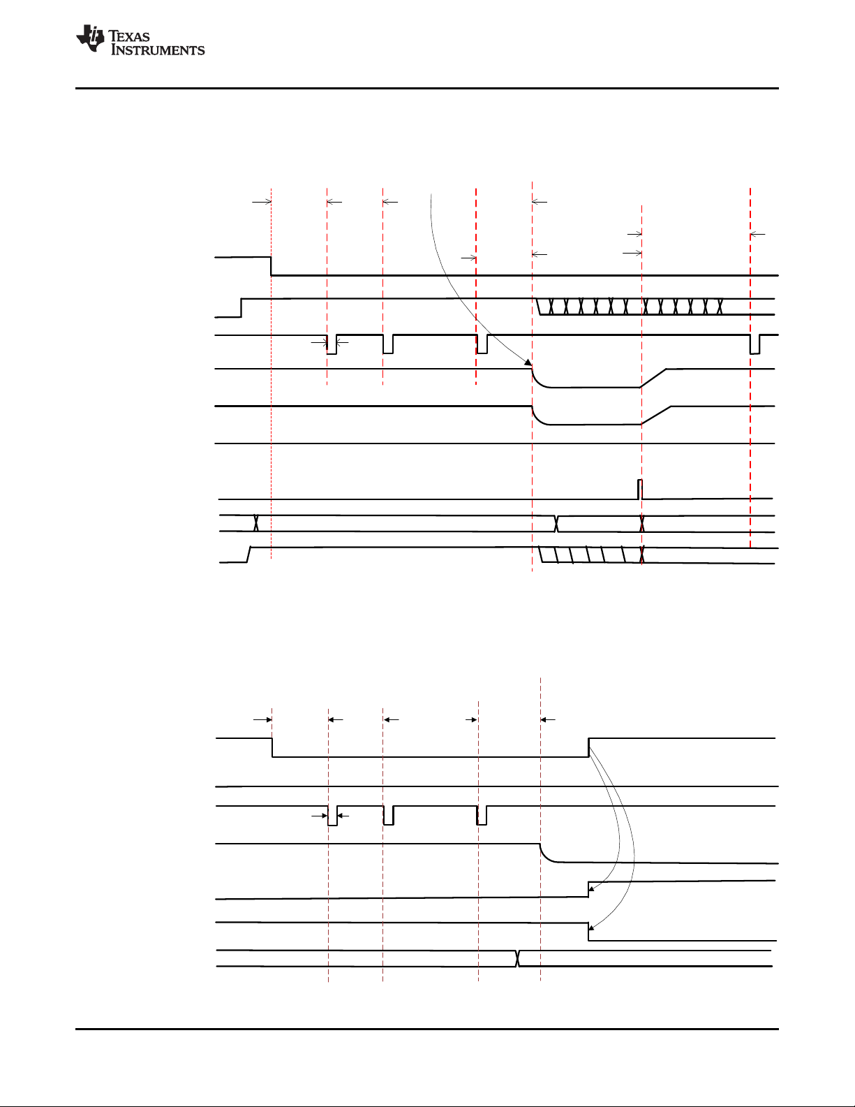
8.3.7.1 MR Wake or Short Button Press Functions
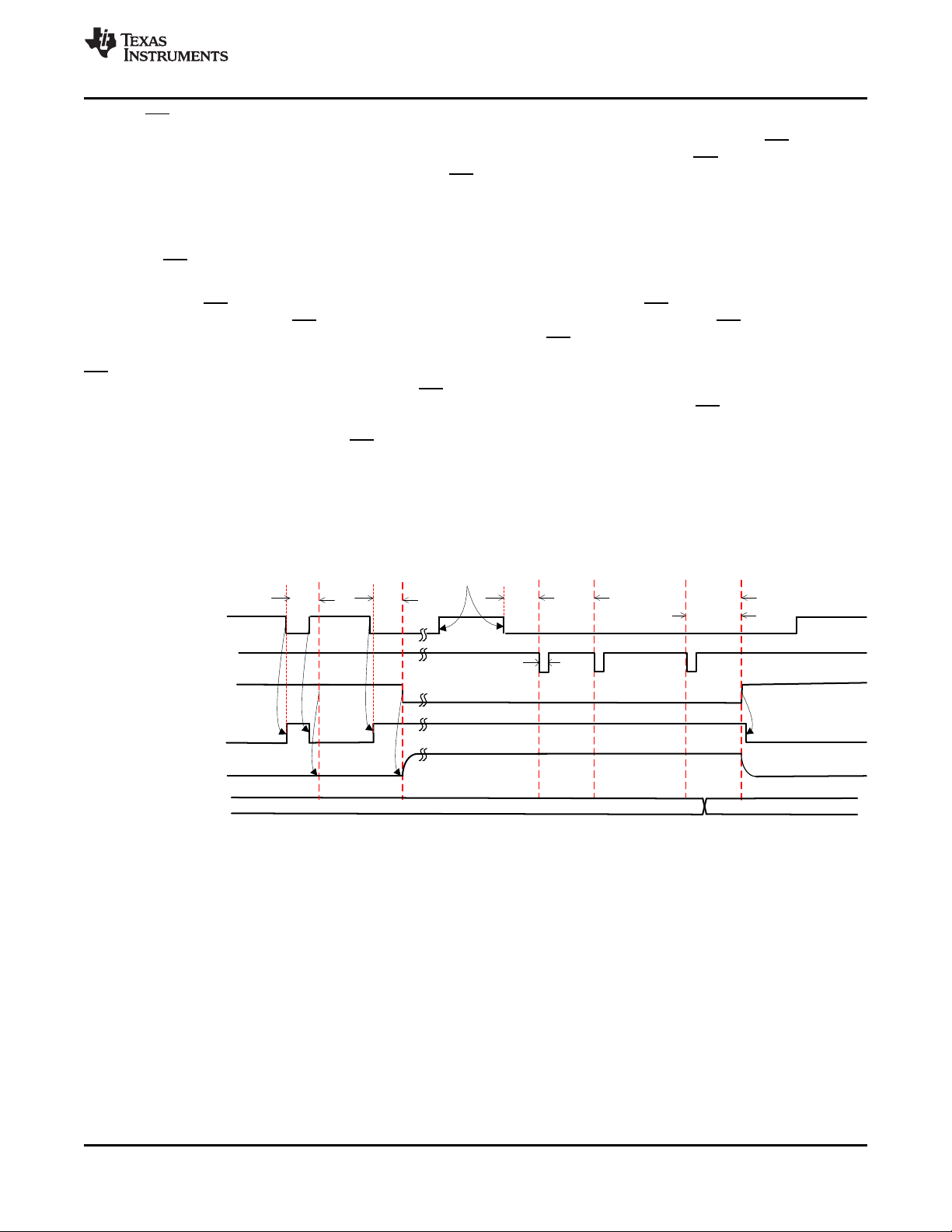
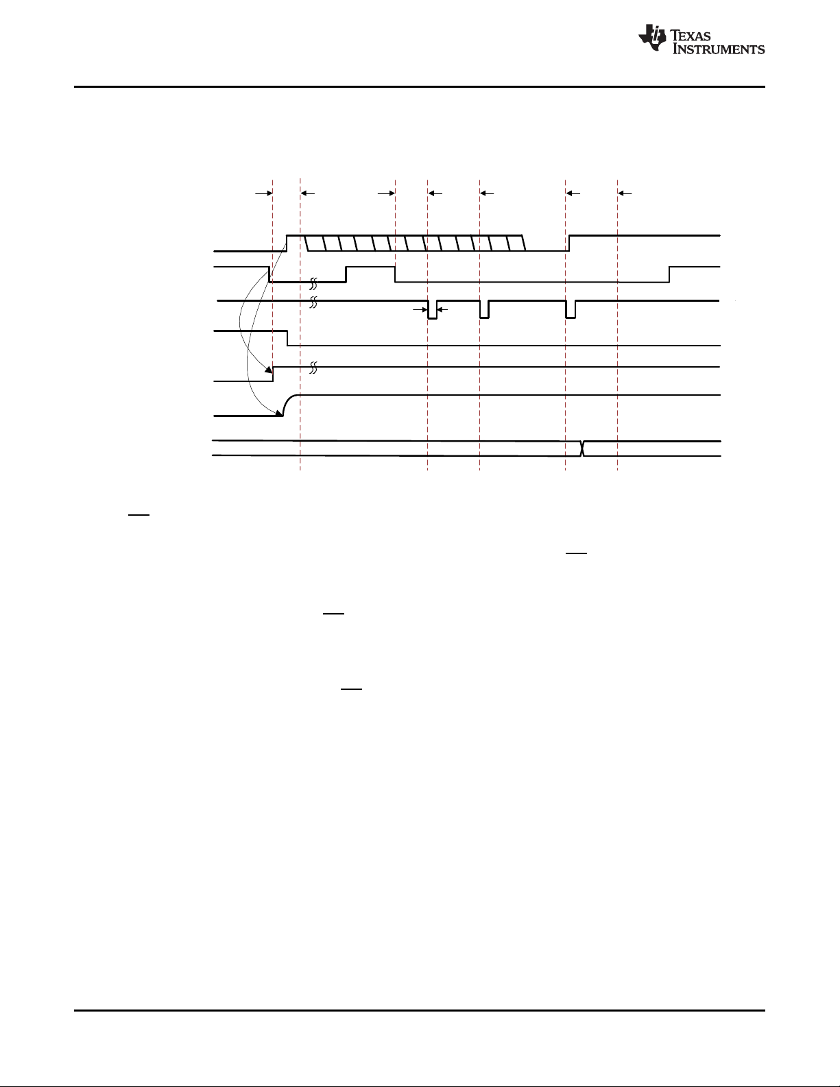
There are two programmable wake or short button press timers, WAKE1 and WAKE2. When the MR pin is held
low for t
WAKE1
the device sends an interrupt (128us active low pulse in the INT pin) and sets the
MRWAKE1_TIMEOUT flag when it expires. If the MR pin continues to be driven low after WAKE1 and the
WAKE2 timer expires, BQ25150 sends a second interrupt and sets the MRWAKE2_TIMOUT flag. WAKE2 is
used as the timer to wake the device from ship mode. WAKE2’s only function is to send the interrupt and has no
effect on other BQ25150 functions. These flags are not cleared until they have been read by the host. Note that
interrupts are only sent when the flags are set and the flags must be cleared in order for another interrupt to be
sent upon MR press. The timer durations can be set through the MR_WAKEx_TIMER bits in the MRCTRL
register.
One of the main MR functions is to wake the device from Ship Mode when the MR is asserted. The device will
exit the Ship Mode when the MR pin is held low for at least t
. Immediately after the MR is asserted, VDD
WAKE2
will be enabled and the digital will start the WAKE counter. If the MR signal remains low until after the WAKE2
timer expires, the device will power up PMID and LDO (If enabled) completing the exit from the ship mode. If the
MR signal goes high before the WAKE2 timer expires, the device will go back to the Ship Mode operation, never
powering up PMID or the LDO. Note that if the MR pin remains low after exiting Ship Mode the wake interrupts
will not be sent and the long button press functions like HW reset will not occur until the MR pin is toggled. In the
case where a valid VIN(VIN> V
) is connected prior to WAKE2 timer expiring, the device will exit the ship
UVLO
mode immediately regardless of the MR or wake timer state. Figure 15 and Figure 16 show these different
scenarios.
Figure 15. MR Wake from Ship Mode (MR_LPRESS_ACTION = Ship Mode, VIN not valid)
Product Folder Links: BQ25150
Submit Documentation FeedbackCopyright © 2018–2019, Texas Instruments Incorporated
23
/MR
INT
SHIPMODE
VDD
twake1
twake2
treset_warn
thwreset
128us
twake1
Output Rails
(PMID, LDO if enabled)
VIN
MR_LPRESS_ACTION
Go to Ship Mode
'RQ¶WFDUH
BQ25150
SLUSD04B –JULY 2018–REVISED FEBRUARY 2019
www.ti.com
Figure 16. MR Wake from Ship Mode – VIN dependencies
8.3.7.2 MR Reset or Long Button Press Functions
The BQ25150 device may be configured to perform a system hardware reset (Power Cycle/Autowake), go into
Ship Mode, or simply do nothing after a long button press (i.e. when the MR pin is driven low until the
MR_HW_RESET timer expires).The action taken by the device when the timer expires is configured through the
MR_LPRESS_ACTION bits in the ICCTRL1 register. Once the MR_HW_RESET timer expires the device
immediately performs the operation set by the MR_LPRESS_ACTION bits. The BQ25150 sends an interrupt to
the host when the device detects that MR has been pressed for a period that is within t
reaching t
HW_RESET
. This may warn the host that the button has been pressed for a period close to t
HW_RESET_WARN
from
HW_RESET
which would trigger a HW Reset or used as another button press timer interrupt like the WAKE1 and WAKE2
timers. This interrupt is sent before the MR_HW_RESET timer expires and sets the MRRESET_WARN flag. The
t
HW_RESET_WARN
may be set through I2C by the MR_RESET_WARN bits in the MRCTRL register. The host may
change the reset behavior at any time after MR going low and prior to the MR_HW_RESET timer expiring. It may
not change it however from another behavior to a HW reset (Power Cycle/Autowake) since a HW reset can be
gated by other condition requirements, such as VIN presence (controlled by MR_RESET_VIN bit), throughout the
whole duration of the button press. This flexibility allows the host to abort any reset or power shutdown to the
system by overriding a long button press command.
A HW Reset may also be started by setting the HW_RESET bit. Note that during a HW reset , VDD remains on.
24
Submit Documentation Feedback Copyright © 2018–2019, Texas Instruments Incorporated
Product Folder Links: BQ25150
/MR
INT
SHIPMODE
VDD
twake1
twake2
Treset_warn
thwreset
128us
PMID & LDO
Shipmode enabled when both
MR has gone high and
thwreset has expired
VIN
MR_RESET_VIN has no effect
on this mode
MR_LPRESS_ACTION
'RQ¶WFDUH
Go to Shipmode
/MR
INT
PMID
LDO
VDD
SW reset
twake1
twake2
treset_
warn
thwreset
t_restart
128us
twake1
VIN
Once thwreset timer
expires and decision to
power cycle is done,
BQ2515x will always
complete the wake
after t_restart, no
matter change in VIN,
or bit control
MR_LPRESS_ACTION
'RQ¶WFDUH
00 - PowerCycle (AutoWake)
MR_RESET_VIN
Default
Default
www.ti.com
BQ25150
SLUSD04B –JULY 2018–REVISED FEBRUARY 2019
Figure 17. MR Wake and Reset Timing with VIN present or BAT Active Mode When MR_LPRESS_ACTION
Figure 18. MR Wake and Reset Timing Active Mode When MR_LPRESS_ACTION = 1x (Ship Mode) and
= 00
Only BAT is Present
Product Folder Links: BQ25150
Submit Documentation FeedbackCopyright © 2018–2019, Texas Instruments Incorporated
25

R/W
VIN
SHIPMODE
VDD
I2C
HWRESET_14S_WD
PMID
14s 14s
R/W
14s
R/W
HW Reset due to no I2C
transaction after VIN
detected
No HW Reset since
function was not reenabled after boot up
No HW Reset since I2C
transaction occurred
within 14s window of
VIN detection
BQ25150
SLUSD04B –JULY 2018–REVISED FEBRUARY 2019
www.ti.com
8.3.8 14-second Watchdog for HW Reset
The BQ25150 integrates 14-second watchdog timer makes the BQ25150 to perform a HW reset/power cycle if
no I2C transaction is detected within 14 seconds of a valid adapter being connected. If the adapter is connected
and the host responds with an I2C transaction before the 14-second watchdog window expires, the part
continues in normal operation. The 14-second watchdog is disabled by default may be enabled through I2C by
setting the HWRESET_14S_WD bit. Figure 19 shows the basic functionality of this feature.
Figure 19. 14-second Watchdog for HW Reset Behavior
8.3.9 Faults Conditions and Interrupts (INT)
The device contains an open-drain output that signals an interrupt and is valid only after the device has
completed start-up into a valid state. If the part starts into a fault, interrupts will not be sent. The INT pin is
normally in high impedance and is pulled low for 128us when an interrupt condition occurs. When a fault or
status change occurs or any other condition that generates an interrupt such as ADC DATA READY, a 128us
pulse (interrupt) is sent on INT to notify the host. All interrupts may be masked through I2C. If the interrupt
condition occurs while the interrupt is masked an interrupt pulse will not be sent. If the interrupt is unmasked
while the fault condition is still present, an interrupt pulse will not be sent until the INT trigger condition occurs
while unmasked.
8.3.9.1 Flags and Fault Condition Response
The table below details the BQ25150 behavior when a fault conditions occurs.
Table 5. Interrupt Triggers and Fault Condition Response
INTERRUPT
FAULT / FLAG DESCRIPTION
CHRG_CV_FLA
G
CHARGE_DONE
_FLAG
IINLIM_ACTIVE_
FLAG
VDPPM_ACTIVE
_FLAG
26
Submit Documentation Feedback Copyright © 2018–2019, Texas Instruments Incorporated
Set when charger
enters Constant
Voltage operation
Set when charger
reaches
termination
Set when Input
Current Limit loop
is active
Set when DPPM
loop is active
TRIGGER
BASED ON
STATUS BIT
CHANGE
Rising Edge Enabled No effect N/A
Rising Edge
Rising Edge
Rising Edge
CHARGER
BEHAVIOR
CHARGER
SAFETY TIMER
Paused-
Charging
resumes with
VIN or CE
Reset N/A
toggle or when
V
is reached
RCH
Enabled.
Reduced
charge current.
Enabled.
Reduced
charge current.
Doubled if option
is enabled
Doubled if option
is enabled
Product Folder Links: BQ25150
LS/LDO
BEHAVIO
R
N/A
N/A
PMID
BEHAVIOR
IN powered if
VINis valid
IN powered if
VINis valid
IN powered VIN
powered unless
supplement
mode condition
is met.
VIN powered
unless
supplement
mode condition
is met.
NOTES

www.ti.com
Table 5. Interrupt Triggers and Fault Condition Response (continued)
FAULT / FLAG DESCRIPTION
VINDPM_ACTIV
E_FLAG
THERMREG_AC
TIVE
VIN_PGOOD_FL
AG
VIN_OVP_FAUL
T_FLAG
BAT_OCP_FAUL
T_FLAG
BAT_UVLO_FAU
LT_FLAG
TS_COLD_FLAG
TS_COOL_FLAG
TS_WARM_FLA
G
TS_HOT_FLAG
ADC_READY_FL
AG
COMP1_ALARM
_FLAG
COMP2_ALARM
_FLAG
COMP3_ALARM
_FLAG
Set when
VINDPM loop is
active
Set when
Thermal Charge
Current Foldback
(Thermal
Regulation) loop
is active
Set when VIN
changes PGOOD
status
Set when VIN>
V
OVP
Set when I
I
BATOCP
Set when V
V
BATUVLO
Set when VTS>
V
TS_COLD
Set when
V
TS_COLD
V
TS_COOL
> VTS>
Set when
V
TS_HOT
V
TS_WARM
< VTS<
Set when VTS<
V
HOT
Set when ADC
conversion is
completed
Set when ADC
measurement
meets
programmed
condition
Set when ADC
measurement
meets
programmed
condition
Set when ADC
measurement
meets
programmed
condition
BAT
BAT
SLUSD04B –JULY 2018–REVISED FEBRUARY 2019
INTERRUPT
TRIGGER
BASED ON
STATUS BIT
CHARGER
BEHAVIOR
CHARGER
SAFETY TIMER
LS/LDO
BEHAVIO
R
CHANGE
Rising Edge
Rising Edge
Enabled.
Reduced
charge current.
Enabled.
Reduced
charge current.
Doubled if option
is enabled
Doubled if option
is enabled
N/A
N/A
If
Rising and
Falling Edge
VIN_PGOOD_S
TAT is low,
charging is
Reset N/A
disabled.
Charging is
Rising Edge
paused until
condition
Reset N/A BAT powered
disappears
>
Rising Edge
<
Rising Edge Enabled No effect N/A
Disabled (BAT
only condition)
N/A N/A Disconnect BAT
Charging
Rising Edge
paused until
condition is
Paused N/A
cleared
Rising Edge
Enabled.
Reduced
charge current.
Doubled if option
is enabled
N/A
Enabled.
Rising Edge
Reduce battery
regulation
No effect N/A
voltage.
Charging
Rising Edge
paused until
condition is
Paused N/A
cleared
Rising Edge N/A N/A N/A N/A
Rising Edge N/A N/A N/A N/A
Rising Edge N/A N/A N/A N/A
Rising Edge N/A N/A N/A N/A
PMID
BEHAVIOR
VIN powered
unless
supplement
mode condition
is met.
VIN powered
unless
supplement
mode condition
is met.
VIN powered (if
VIN_PGOOD_S
TAT=1) unless
PMID_MODE is
not 00.
IN powered of
VINis valid
IN powered of
VINis valid
IN powered of
VINis valid
IN powered of
VINis valid
IN powered of
VINis valid
BQ25150
NOTES
Interrupt will not
be sent if device
powers up with
VIN_PGOOD
condition and
V
<
BAT
V
BATUVLO
Product Folder Links: BQ25150
Submit Documentation FeedbackCopyright © 2018–2019, Texas Instruments Incorporated
27

BQ25150
SLUSD04B –JULY 2018–REVISED FEBRUARY 2019
Table 5. Interrupt Triggers and Fault Condition Response (continued)
INTERRUPT
FAULT / FLAG DESCRIPTION
Set when charge
IMAX_ACTIVE_F
LAG
TS_OPEN_FLAG
WD_FAULT_FLA
G
SAFETY_TMR_F
AULT_FLAG
LS_LDO_OCP_F
AULT_FLAG
IMAX_FAULT_FL
AG
MRWAKE1_TIM
EOUT_FLAG
MRWAKE2_TIM
EOUT_FLAG
MRRESET_WAR
N_FLAG
TSHUT
current is
programmed
above the IMAX
setting
Set when VTS>
V
TS_OPEN
Set when I2C
watchdog timer
expires
Set when safety
Timer expires.
Cleared after VIN
or CE toggle
Set when LDO
output current
exceeds OCP
condition
Set when a an
open is detected
on IMAX pin
Set when MR is
low for at least
t
WAKE1
Set when MR is
low for at least
t
WAKE2
Set when MR is
low for at least
t
RESETWARN
No flag. Die
temperature
exceeds thermal
shutdown
threshold is
reached
TRIGGER
BASED ON
STATUS BIT
CHANGE
Rising Edge Enabled N/A N/A N/A
Rising Edge
Rising Edge Enabled N/A N/A N/A
Rising Edge
Rising Edge N/A N/A
Rising Edge
Rising Edge N/A N/A N/A N/A
Rising Edge N/A N/A N/A N/A
Rising Edge N/A N/A N/A N/A
N/A Disabled Disabled Disabled Disabled
CHARGER
BEHAVIOR
Charging is
paused until
condition
disappears
Disabled until
VIN or CE
toggle
Chareg disabled
until Power-On-
Reset
CHARGER
SAFETY TIMER
Paused N/A N/A
Reset after flag is
cleared
N/A N/A N/A
LS/LDO
BEHAVIO
R
N/A
Enabled
(host must
take action
to disable
the LDO if
desired)
PMID
BEHAVIOR
IN powered of
VINis valid
N/A
www.ti.com
NOTES
8.3.10 Power Good (PG) Pin
The PG pin is an open-drain output that by default indicates when a valid IN supply is present. It may also be
configured to be a general purpose output (GPO) controlled through I2C or to be a level shifted version of the MR
input signal. Connect PG to the desired logic voltage rail using a 1-kΩ to 100-kΩ resistor, or use with an LED for
visual indication. Below is the description for each configuration:
• In its default state, PG pulls to GND when the following conditions are met: VIN> V
VIN< V
. PG is high impedance when the input power is not within specified limits.
IN_OVP
UVLO
, VIN> V
BAT+VSLP
and
• MR shifted (MRS) output when the PG_MODE bits are set to 01. PG is high impedance when the MR input is
high, and PG pulls to GND when the MR input is low.
• General purpose open drain output when setting the PG_MODE bits to 1x. The state of the PG pin is then
controlled through the GPO_PG bit, where if GPO_PG is 0 , the PG pin is pulled to GND and if it is 1, the PG
pin is in high impedance.
28
Submit Documentation Feedback Copyright © 2018–2019, Texas Instruments Incorporated
Product Folder Links: BQ25150
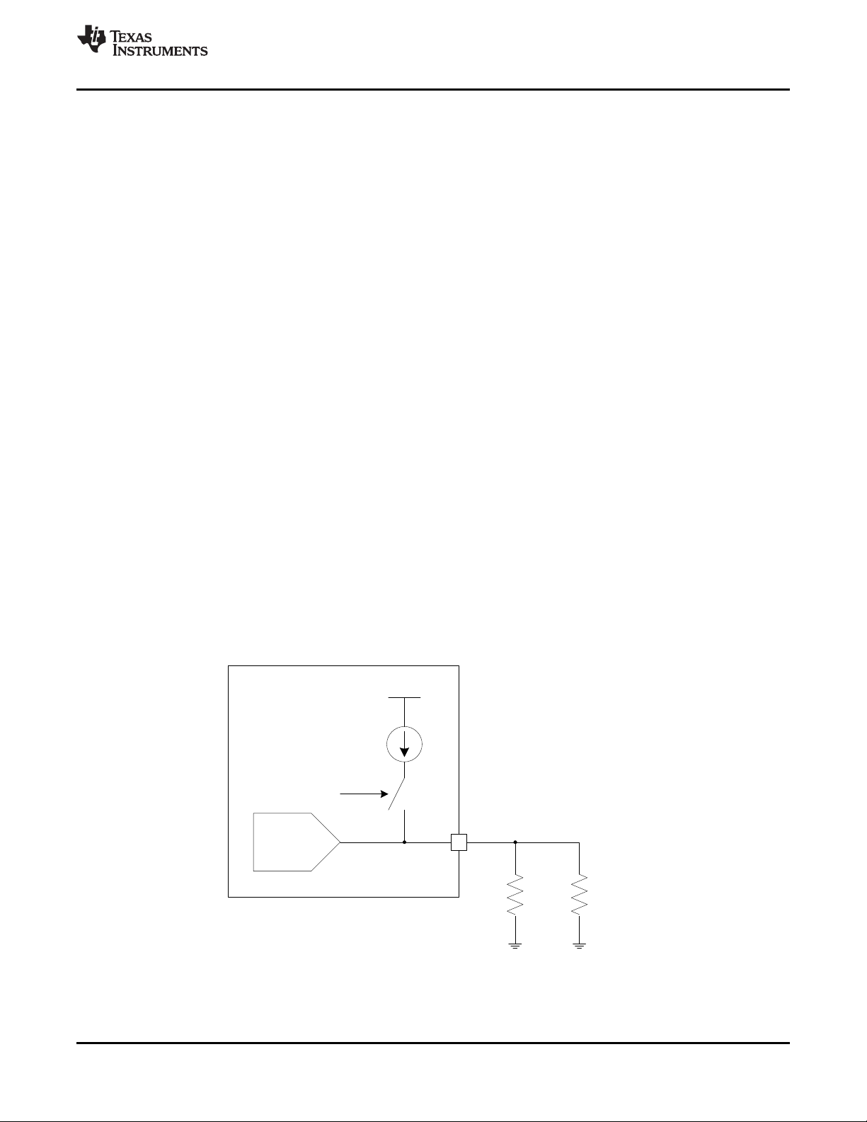
BQ25150
TS
VDD
NTC R
PARALLEL
R
PARALLEL
= R
NTC@25C
ADC
TS
measurement
control
TS I
BIAS
BQ25150
www.ti.com
SLUSD04B –JULY 2018–REVISED FEBRUARY 2019
8.3.11 External NTC Monitoring (TS)
The I2C interface allows the user to easily implement the JEITA standard for systems where the battery pack
thermistor is monitored by the host. Additionally, the device provides a flexible voltage based TS input for
monitoring the battery pack NTC thermistor. The voltage at TS is monitored to determine that the battery is at a
safe temperature during charging.
The part can be configured to meet JEITA requirements or a simpler HOT/COLD function only. Additionally, the
TS charger control function can be disabled. To satisfy the JEITA requirements, four temperature thresholds are
monitored: the cold battery threshold, the cool battery threshold, the warm battery threshold, and the hot battery
threshold. These temperatures correspond to the V
Characteristics table. Charging and safety timers are suspended when VTS< V
VTS< V
, the charging current is reduced to the value programmed in the TS_FASTCHGCTRL register. Note
COLD
COLD
, V
COOL
, V
WARM
, and V
HOT
thresholds in the Electrical
HOT
or VTS> V
COLD
. When V
COOL
that the current steps for fast charge in the COOL region, just as those in normal fast charge, are multiples of the
fast charge LSB value (1.25mA by default). So in the case where the calculated scaled down current for the
COOL region falls in between charge current steps, the device will round down the charge current to the nearest
step. For example, if the fast charge current is set for 15mA (ICHG = 1100) and TS_FASTCHARGE =111
(0.125*ICHG), the charge current in the COOL region will be 1.25mA instead of the calculated 1.85mA.
When V
< VTS< V
HOT
, the battery regulation voltage is reduced to the value programmed in the
WARM
TS_FASTCHGCTRL register.
Regardless of whether the part is configured for JEITA, HOT/COLD, or disabled, when a TS fault occurs, a
128us pulse is sent on the INT output, and the FAULT bits of the register are updated over I2C. The FAULT bits
are not cleared until they are read over I2C. This allows the host processor to take action if a different behavior
than the pre-set function is needed. Alternately, the TS pin voltage can be read by the host if VIN is present or
when BAT is present, so the appropriate action can be taken by the host.
<
8.3.11.1 TS Thresholds
The BQ25150 monitors the TS voltage and sends an interrupt to the host whenever it crosses the V
V
COOL
and V
thresholds which correspond to different temperature thresholds based on the NTC resistance
COLD
HOT
and biasing. These thresholds may be adjusted through I2C by the host. The device will also disable charging if
TS pin exceeds the V
TS_OPEN
threshold.
The TS biasing circuit is shown in Figure 20. The ADC range is set to 1.2 V. Note that the respective VTSand
hence ADC reading for T
COLD
(0°C), T
COOL
(10°C), T
WARM
(45°C) and T
(60°C) changes for every NTC,
HOT
therefore the threshold values may need to be adjusted through I2C based on the supported NTC type.
, V
WARM
,
Figure 20. TS Bias Functional Diagram
Product Folder Links: BQ25150
Submit Documentation FeedbackCopyright © 2018–2019, Texas Instruments Incorporated
29
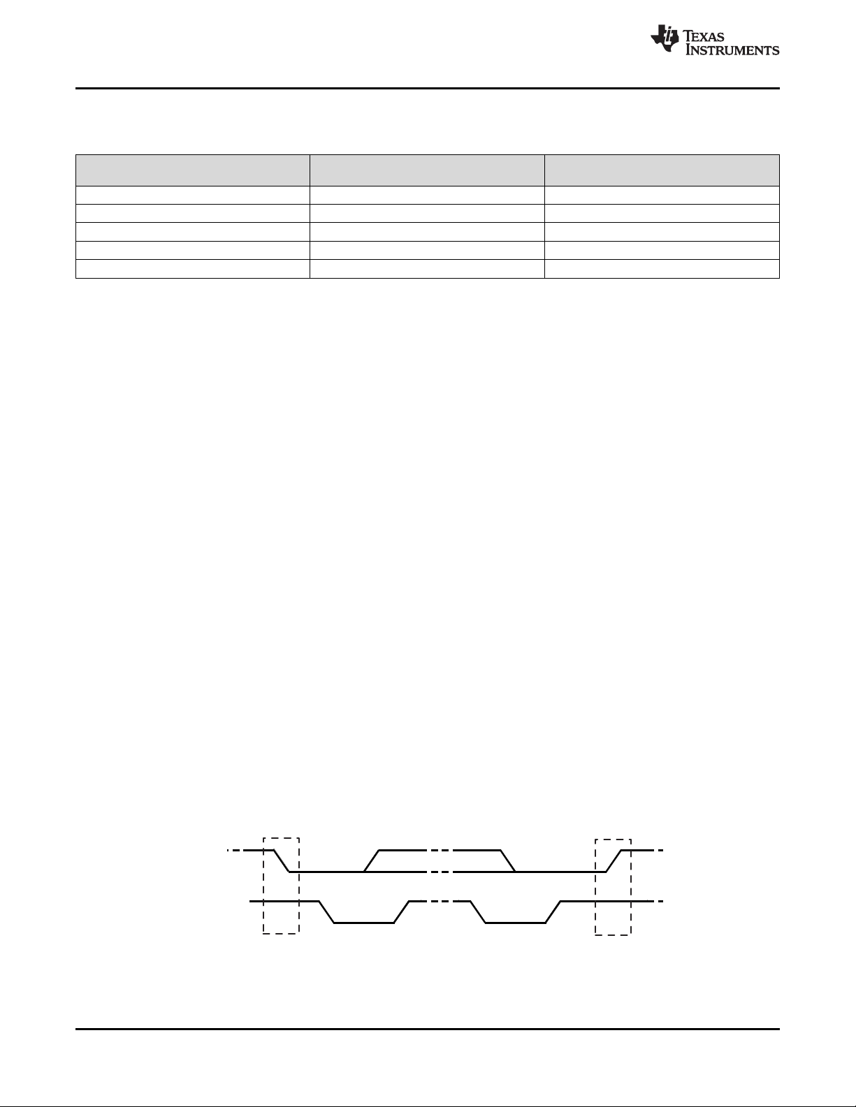
START Condition
DATA
CLK
STOP Condition
S
P
BQ25150
SLUSD04B –JULY 2018–REVISED FEBRUARY 2019
www.ti.com
The BQ25150 supports by default the following thresholds for a 10KΩ NTC
Table 6. TS Thresholds for 10K Thermistor
THRESHOLD
Open -- >0.9
Cold 0 0.585
Cool 10 0.514
Warm 45 0.265
Hot 60 0.185
TEMPERATURE
(°C)
VTS (V)
For accurate temperature thresholds a 10K NTC with a 3380 B-constant should be used (Murata
NCP03XH103F05RL for example) with a parallel 10K resistor. Each threshold can be programmed via I2C
through the TS_COLD, TS_COOL, TS_WARM and TS_HOT registers. The value in the registers corresponds to
the 8 MSBs in the TS ADC output code.
8.3.12 External NTC Monitoring (ADCIN)
The ADCIN pin can be configured through I2C to support NTC measurements without the need of an external
biasing circuit. In this mode, the ADCIN pin is biased and monitored in the same manner as the TS pin.
Measurement data can be read by selecting one of the ADC data slots to read the ADCIN.
8.3.13 I2C Interface
The BQ25150 device uses a fully compliant I2C interface to program and read control parameters, status bits,
etc. I2C ™ is a 2-wire serial interface developed by Philips Semiconductor (see I2C-Bus Specification, Version
2.1, January 2000). The bus consists of a data line (SDA) and a clock line (SCL) with pull-up structures. When
the bus is idle, both SDA and SCL lines are pulled high. All the I2C compatible devices connect to the I2C bus
through open drain I/O pins, SDA and SCL. A master device, usually a microcontroller or a digital signal
processor, controls the bus. The master is responsible for generating the SCL signal and device addresses. The
master also generates specific conditions that indicate the START and STOP of data transfer. A slave device
receives and/or transmits data on the bus under control of the master device.
BQ25150 works as a slave and supports the following data transfer modes, as defined in the I2C Bus™
Specification: standard mode (100 kbps) and fast mode (400 kbps). The interface adds flexibility to the battery
charge solution, enabling most functions to be programmed to new values depending on the instantaneous
application requirements.
Register contents remain intact as long as VBAT or VIN voltages remains above their respective UVLO levels.
The data transfer protocol for standard and fast modes is exactly the same; therefore, they are referred to as the
F/S-mode in this document. The BQ25150 device 7-bit address is 0×6B (shifted 8-bit address is 0xD6).
8.3.13.1 F/S Mode Protocol
The master initiates data transfer by generating a start condition. The start condition is when a high-to-low
transition occurs on the SDA line while SCL is high, as shown in Figure 21. All I2C-compatible devices should
recognize a start condition.
Figure 21. START and STOP Condition
30
Submit Documentation Feedback Copyright © 2018–2019, Texas Instruments Incorporated
Product Folder Links: BQ25150
 Loading...