

Texas Instruments bq24707, bq24707A Datasheet
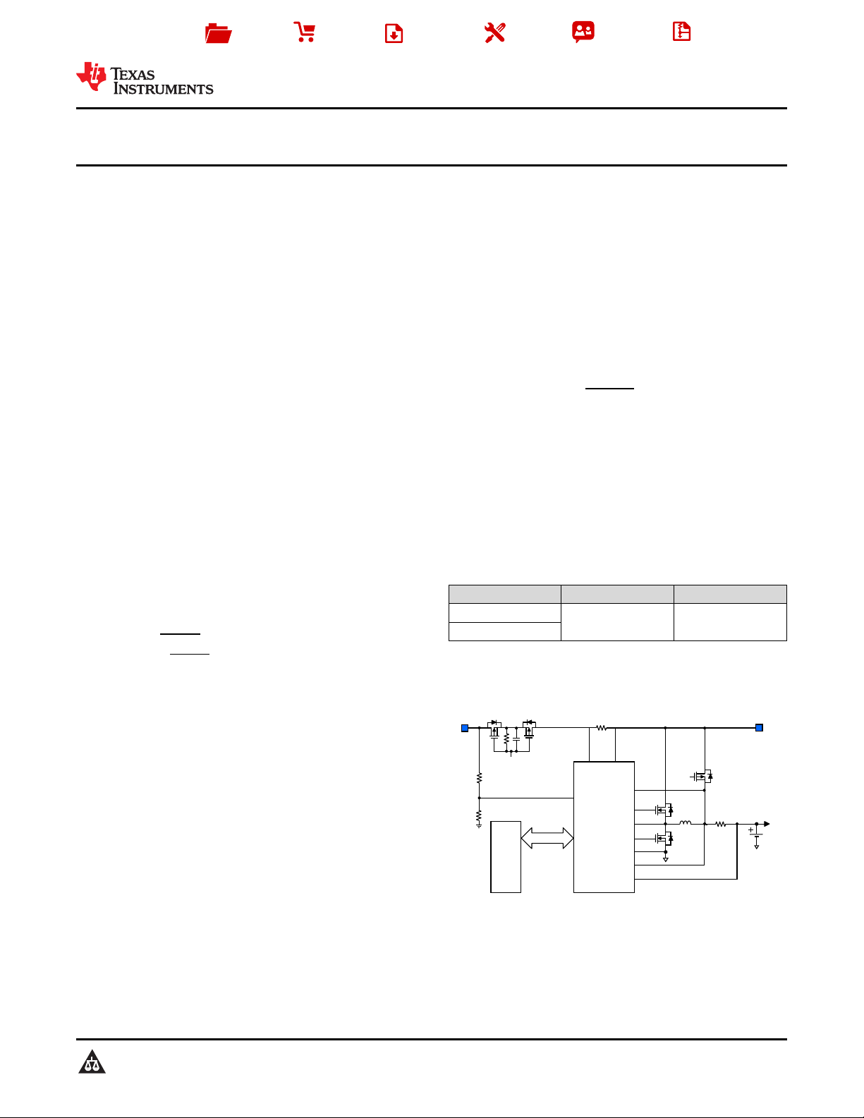
R
SR
Adapter
4.5-24 V
HOST
bq2707x
SYS
Battery
Pack
1S-4S
SMBus
SMBus Controls V & I
with high accuracy
Adapter Detection
Enhanced Safety:
OCP,OVP,FET Short
Integration:
Loop Compensation; Soft-Start
Comparator
R
AC
Charge
Controller
P P
Q1 Q2
Product
Folder
Sample &
Buy
Technical
Documents
Tools &
Software
Support &
Community
Reference
Design
bq24707,bq24707A
SLUSA78C –JULY 2010–REVISED JULY 2015
bq24707x 1-4 Cell Li+ Battery SMBus Charge Controller With Independent Comparator
and Advanced Circuit Protection
1 Features 3 Description
1
• SMBus Host-Controlled NMOS-NMOS
Synchronous Buck Converter With Programmable
615 kHz, 750 kHz, and 885 kHz Switching
Frequency
• Real-Time System Control on ILIM Pin to Limit
Charge Current
• Enhanced Safety Features for Overvoltage
Protection, Overcurrent Protection, Battery,
Inductor, and MOSFET Short-Circuit Protection
• Programmable Input Current, Charge Voltage,
Charge Current Limits
– ±0.5% Charge Voltage Accuracy up to 19.2 V
– ±3% Charge Current Accuracy up to 8.128 A
– ±3% Input Current Accuracy up to 8.064 A
– ±2% 20× Adapter Current or Charge Current
Output Accuracy
• Programmable Adapter Detection and Indicator
• Independent Comparator With Internal Reference
• Integrated Soft-Start
• Integrated Loop Compensation
• AC Adapter Operating Range 5 V to 24 V
• 15-µA Off-State Battery Discharge Current
• 20-pin 3.5 mm × 3.5 mm QFN Package
• bq24707: ACOK Delay Default 1.3 s
• bq24707A: ACOK Delay Default 1.2 ms
The bq24707 and bq24707A devices are highefficiency, synchronous battery chargers, offering low
component count for space-constrained, multichemistry battery charging applications.
SMBus controlled input current, charge current, and
charge voltage DACs allow for very high regulation
accuracies that can be easily programmed by the
system power management micro-controller.
The IC uses the internal input current register or
external ILIM pin to throttle down PWM modulation to
reduce the charge current.
The IC provides an IFAULT output to alarm if any
MOSFET fault or input over current occurs. This
alarm output allows users to turn off input power
selectors when the fault occurs. Meanwhile, an
independent comparator with internal reference is
available to monitor input current, output current, or
output voltage.
The IC charges one-, two-, three-, or four-series Li+
cells, and is available in a 20-pin, 3.5 × 3.5 mm QFN
package.
Device Information
PART NUMBER PACKAGE BODY SIZE (NOM)
bq24707
bq24707A
(1) For all available packages, see the orderable addendum at
the end of the data sheet.
VQFN (20) 3.50 mm × 3.50 mm
(1)
2 Applications
• Portable Notebook Computers, UMPCs, Ultra-Thin
Notebooks, and Netbooks
• Personal Digital Assistants
• Handheld Terminals
• Industrial and Medical Equipment
• Portable Equipment
1
An IMPORTANT NOTICE at the end of this data sheet addresses availability, warranty, changes, use in safety-critical applications,
intellectual property matters and other important disclaimers. PRODUCTION DATA.
Simplified Schematic

bq24707,bq24707A
SLUSA78C –JULY 2010–REVISED JULY 2015
www.ti.com
Table of Contents
1 Features .................................................................. 1
2 Applications ........................................................... 1
3 Description ............................................................. 1
4 Revision History..................................................... 2
5 Device Comparison Table..................................... 3
6 Pin Configuration and Functions......................... 3
7 Specifications......................................................... 5
7.1 Absolute Maximum Ratings...................................... 5
7.2 ESD Ratings.............................................................. 5
7.3 Recommended Operating Conditions....................... 5
7.4 Thermal Information.................................................. 5
7.5 Electrical Characteristics........................................... 6
7.6 Timing Requirements.............................................. 10
7.7 Typical Characteristics............................................ 11
8 Detailed Description............................................ 14
8.1 Overview................................................................. 14
8.2 Functional Block Diagram....................................... 15
8.3 Feature Description................................................. 16
8.4 Device Functional Modes........................................ 17
8.5 Programming........................................................... 18
9 Application and Implementation ........................ 26
9.1 Application Information............................................ 26
9.2 Typical Application ................................................. 26
10 Power Supply Recommendations..................... 31
11 Layout................................................................... 31
11.1 Layout Guidelines ................................................. 31
11.2 Layout Example .................................................... 33
12 Device and Documentation Support ................. 35
12.1 Device Support...................................................... 35
12.2 Documentation Support ........................................ 35
12.3 Related Links ........................................................ 35
12.4 Community Resources.......................................... 35
12.5 Trademarks........................................................... 35
12.6 Electrostatic Discharge Caution............................ 35
12.7 Glossary................................................................ 35
13 Mechanical, Packaging, and Orderable
Information........................................................... 36
4 Revision History
NOTE: Page numbers for previous revisions may differ from page numbers in the current version.
Changes from Revision B (March 2011) to Revision C Page
• Added ESD Ratings table, Feature Description section, Device Functional Modes, Application and Implementation
section, Power Supply Recommendations section, Layout section, Device and Documentation Support section, and
Mechanical, Packaging, and Orderable Information section.................................................................................................. 1
Changes from Revision A (November 2010) to Revision B Page
• Added Features for the bq24707 and bq24707A .................................................................................................................. 1
• Added device bq24707A to this data sheet............................................................................................................................ 1
• Added bq24707A to the ORDERING INFORMATION table.................................................................................................. 3
• Added the COMPARISON TABLE......................................................................................................................................... 3
• Added bq24707 only to the test condition of t
• Added bq24707A only to the test condition of t
ACOK_FALL_DEG
ACOK_FALL_DEG
first row.................................................................................... 10
second row............................................................................ 10
• Added (bq24707) to the title of Figure 2............................................................................................................................... 11
• Added a new paragraph in the Battery Over Voltage Protection (BATOVP) section........................................................... 17
• Changed the Description of the ACOK Deglitch Time Adjust bit in Table 3......................................................................... 20
• Changed the Adapter Detect and ACOK Output section. included 1.3s for bq24707 and 1.2ms for bq24707A................. 24
• Changed the Description of item U1 in Table 9 ................................................................................................................... 30
Changes from Original (July 2010) to Revision A Page
• Updated the description for the SRN and SRP pins .............................................................................................................. 4
• Changed the Functional Block Diagram, Figure 16.............................................................................................................. 26
• Added Added section: Negative Output Voltage Protection................................................................................................. 27
• Deleted C12, added R14 and R15 in Table 9...................................................................................................................... 30
2 Submit Documentation Feedback Copyright © 2010–2015, Texas Instruments Incorporated
Product Folder Links: bq24707 bq24707A
1
2
3
4
5
6 7 8 9 10
15
14
13
12
11
20 19 18 17 16
ACN
ACP
CMPOUT
CMPIN
ACOK
ACDET
IOUT
SDA
SCL
ILIM
IFAULT
SRN
SRP
GND
LODRV
REGN
BTST
HIDRV
PHASE
VCC
bq24707
bq24707A
www.ti.com
5 Device Comparison Table
CONDITION bq24707 bq24707A
ACOK default delay 1.3 s 1.2 ms
Suggest fully charged battery ChargeVoltage() setting
after termination
Suggest fully charged battery ChargeCurrent() setting
after termination
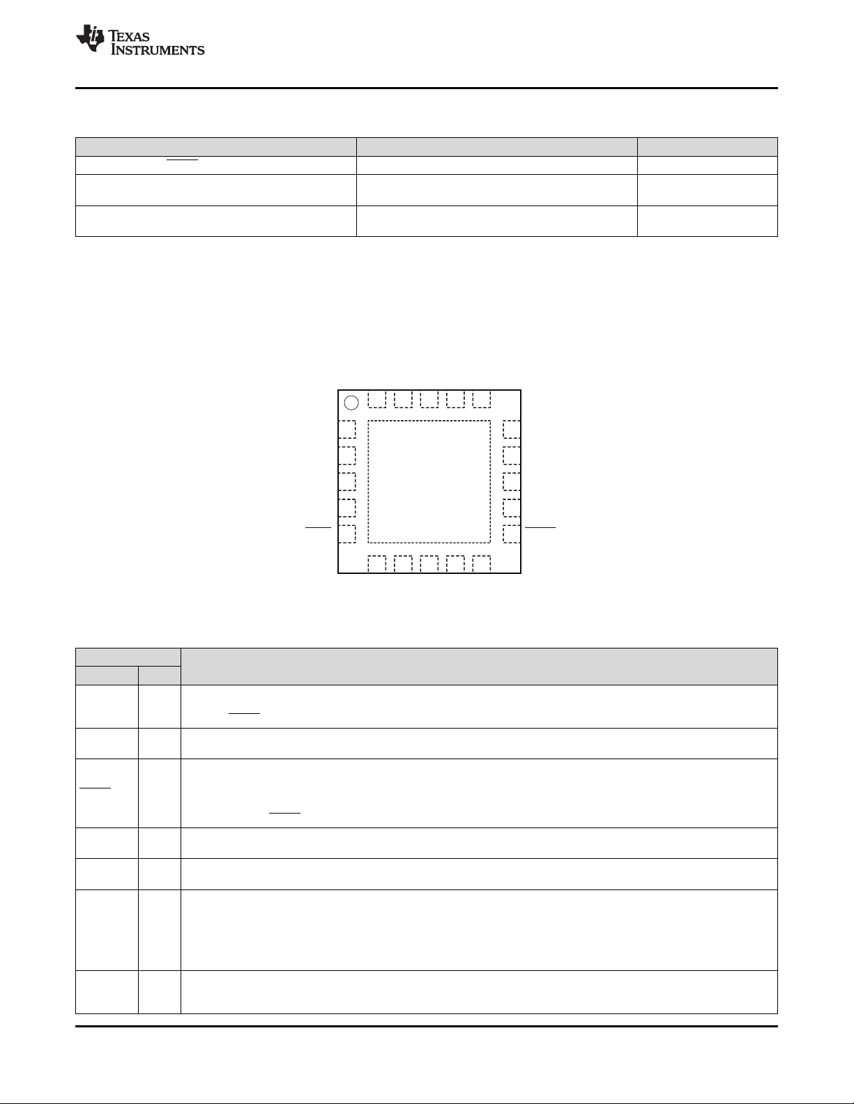
6 Pin Configuration and Functions
bq24707,bq24707A
SLUSA78C –JULY 2010–REVISED JULY 2015
Full scale charge voltage(12.592 V for 3-S battery) 0 V
0 A 0 A
RGR Package
20-Pin VQFN
Top View
Pin Functions
PIN
NAME NO.
Adapter detection input. Program the adapter valid input threshold by connecting a resistor-divider from the adapter
ACDET 6 input to the ACDET pin to the GND pin. When the ACDET pin is above 0.6 V and VCC is above UVLO, REGN LDO is
present, ACOK comparator and IOUT are both active.
ACN 1
Input current-sense resistor negative input. Place an optional 0.1-µF ceramic capacitor from ACN to GND for commonmode filtering. Place a 0.1-µF ceramic capacitor from ACN to ACP to provide differential-mode filtering.
AC adapter detect open-drain output. The output is pulled LOW to GND by an internal MOSFET when the voltage on
the ACDET pin is above 2.4 V, voltage on the VCC pin is above UVLO and voltage on the VCC pin is 245 mV above
ACOK 5 the voltage on the SRN pin, indicating a valid adapter is present to start charge. If any one of the above conditions
cannot meet, it is pulled HIGH to the external pullup supply rail by an external pullup resistor. Connect a 10-kΩ pullup
resistor from the ACOK pin to the pullup supply rail.
ACP 2
BTST 17
CMPIN 4
CMPOUT 3 Internal reference is 0.6 V or 2.4 V, selectable by SMBus command ChargeOption(). When CMPIN is above the
Copyright © 2010–2015, Texas Instruments Incorporated Submit Documentation Feedback 3
Input current-sense resistor positive input. Place a 0.1-µF ceramic capacitor from ACP to GND for common-mode
filtering. Place a 0.1-µF ceramic capacitor from ACN to ACP to provide differential-mode filtering.
High-side power MOSFET driver power supply. Connect a 0.047-µF capacitor from BTST to PHASE, and a bootstrap
Schottky diode from REGN to BTST.
Input of independent comparator. The comparator has one 50-kΏ series resistor and one 2000-kΏ pulldown resistor.
Program CMPIN voltage by connecting a resistor-divider from the IOUT pin to the CMPIN pin to the GND pin for
adapter or charge current comparison or from the SRN pin to the CMPIN pin to the GND pin for battery voltage
comparison. The internal reference is 0.6 V or 2.4 V, selectable by SMBus command ChargeOption(). When CMPIN is
above the internal reference, CMPOUT goes HIGH. Place a resistor between CMPIN and CMPOUT to program
hysteresis.
Open-drain output of independent comparator. Place a 10-kΩ pullup resistor from CMPOUT to pullup supply rail.
internal reference, CMPOUT goes HIGH. Place a resistor between CMPIN and CMPOUT to program hysteresis.
Product Folder Links: bq24707 bq24707A
DESCRIPTION
bq24707,bq24707A
SLUSA78C –JULY 2010–REVISED JULY 2015
www.ti.com
Pin Functions (continued)
PIN
NAME NO.
GND 14
HIDRV 18 High-side power MOSFET driver output. Connect to the high-side N-channel MOSFET gate.
IFAULT 11
ILIM 10
IOUT 7 the differential voltage across the sense resistor. Place a 100-pF or less ceramic decoupling capacitor from the IOUT
LODRV 15 Low-side power MOSFET driver output. Connect to low-side N-channel MOSFET gate.
PHASE 19 High-side power MOSFET driver source. Connect to the source of the high-side N-channel MOSFET.
PowerPAD solder PowerPAD to the board, and have vias on the PowerPAD plane connecting to analog ground and power
REGN 16 voltage on the ACDET pin is above 0.6 V and voltage on VCC is above UVLO. Connect a 1-µF ceramic capacitor from
SCL 9
SDA 8
SRN 12 filtering and connect to current-sensing resistor. Connect a 0.1-µF ceramic capacitor between current sensing resistor
SRP 13
VCC 20
IC ground. On PCB layout, connect to the analog ground plane, and only connect to power ground plane through the
PowerPAD™ underneath the IC.
Open-drain output. The output is pulled LOW by an internal MOSFET when ACOC or a short-circuit is detected. The
output is pulled HIGH to the external pullup supply rail by an external pullup resistor in normal condition.
Charge current-limit input. Program ILIM voltage by connecting a resistor-divider from the system reference 3.3-V rail
to the ILIM pin to the GND pin. The lower of the ILIM voltage or DAC limit voltage sets the charge current regulation
limit. To disable control on ILIM, set ILIM above 1.6 V. Once the voltage on the ILIM pin falls below 75 mV, charge is
disabled. Charge is enabled when the ILIM pin rises above 105 mV.
Buffered adapter or charge current output, selectable with SMBus command ChargeOption(). IOUT voltage is 20 times
pin to GND.
Exposed pad beneath the IC. Analog ground and power ground star-connected only at the PowerPAD plane. Always
ground planes. The pad also serves as a thermal pad to dissipate the heat.
Linear regulator output. REGN is the output of the 6-V linear regulator supplied from VCC. The LDO is active when the
REGN to GND.
SMBus open-drain clock input. Connect to the SMBus clock line from the host controller or smart battery. Connect a
10-kΩ pullup resistor according to SMBus specifications.
SMBus open-drain data I/O. Connect to the SMBus data line from the host controller or smart battery. Connect a 10kΩ pullup resistor according to SMBus specifications.
Charge current-sense resistor negative input. The SRN pin is for battery voltage sensing as well. Connect SRN pin to
a 7.5-Ω resistor first then from resistor another terminal connect a 0.1-µF ceramic capacitor to GND for common-mode
to provide differential-mode filtering. See Application and Implementation about negative output voltage protection for
hard shorts on battery-to-ground or battery-reverse connection by adding small resistor.
Charge current-sense resistor positive input. Connect SRP pin to a 10-Ω resistor first, then, from resistor another
terminal, connect to current-sensing resistor. Connect a 0.1-µF ceramic capacitor between current sensing resistor to
provide differential-mode filtering. See Application and Implementation about negative output voltage protection for
hard shorts on battery-to-ground or battery-reverse connection by adding small resistor.
Input supply, diode OR from adapter or battery voltage. Use 10-Ω resistor and 1-µF capacitor to ground as low pass
filter to limit inrush current.
DESCRIPTION
4 Submit Documentation Feedback Copyright © 2010–2015, Texas Instruments Incorporated
Product Folder Links: bq24707 bq24707A
bq24707,bq24707A
www.ti.com
SLUSA78C –JULY 2010–REVISED JULY 2015
7 Specifications
7.1 Absolute Maximum Ratings
over operating free-air temperature range (unless otherwise noted)
SRN, SRP, ACN, ACP, VCC –0.3 30
PHASE –2 30
Voltage
ACDET, SDA, SCL, LODRV, REGN, IOUT, ILIM, ACOK, IFAULT, CMPIN,
CMPOUT V
BTST, HIDRV –0.3 36
Maximum difference SRP–SRN, ACP–ACN –0.5 0.5
voltage
Junction temperature, T
Storage temperature, T
J
stg
(1) Stresses beyond those listed under Absolute Maximum Ratings may cause permanent damage to the device. These are stress ratings
only, which do not imply functional operation of the device at these or any other conditions beyond those indicated under Recommended
Operating Conditions. Exposure to absolute-maximum-rated conditions for extended periods may affect device reliability.
(2) All voltages are with respect to GND if not specified. Currents are positive into, negative out of the specified terminal. Consult Packaging
Section of the data book for thermal limitations and considerations of packages.
7.2 ESD Ratings
Human body model (HBM), per ANSI/ESDA/JEDEC JS-001
V
(1) JEDEC document JEP155 states that 500-V HBM allows safe manufacturing with a standard ESD control process.
(2) JEDEC document JEP157 states that 250-V CDM allows safe manufacturing with a standard ESD control process.
Electrostatic discharge V
(ESD)
Charged device model (CDM), per JEDEC specification JESD22- ±500
(2)
C101
(1)(2)
MIN MAX UNIT
–0.3 7
–40 155 °C
–55 155 °C
VALUE UNIT
(1)
±2000
7.3 Recommended Operating Conditions
over operating free-air temperature range (unless otherwise noted)
MIN NOM MAX UNIT
SRN, SRP, ACN, ACP, VCC 0 24
PHASE –2 24
Voltage V
Maximum difference voltage SRP–SRN, ACP–ACN –0.2 0.2 V
Junction temperature, T
J
ACDET, SDA, SCL, LODRV, REGN, IOUT, ILIM, ACOK, IFAULT, CMPIN,
CMPOUT
0 6.5
BTST, HIDRV 0 30
0 125 °C
7.4 Thermal Information
bq24707x
THERMAL METRIC
R
R
R
ψ
ψ
R
Junction-to-ambient thermal resistance 46.8 °C/W
θJA
Junction-to-case (top) thermal resistance 56.9 °C/W
θJC(top)
Junction-to-board thermal resistance 46.6 °C/W
θJB
Junction-to-top characterization parameter 0.6 °C/W
JT
Junction-to-board characterization parameter 15.3 °C/W
JB
Junction-to-case (bottom) thermal resistance 4.4 °C/W
θJC(bot)
(1) For more information about traditional and new thermal metrics, see the Semiconductor and IC Package Thermal Metrics application
report, SPRA953.
(1)
RGR [VQFN] UNIT
20 PINS
Copyright © 2010–2015, Texas Instruments Incorporated Submit Documentation Feedback 5
Product Folder Links: bq24707 bq24707A
bq24707,bq24707A
SLUSA78C –JULY 2010–REVISED JULY 2015
7.5 Electrical Characteristics
4.5 V ≤ V
OPERATING CONDITIONS
V
VCC_OP
CHARGE VOLTAGE REGULATION
V
BAT_REG_RNG
V
BAT_REG_ACC
CHARGE CURRENT REGULATION
V
IREG_CHG_RNG
I
CHRG_REG_ACC
INPUT CURRENT REGULATION
V
IREG_DPM_RNG
I
DPM_REG_ACC
INPUT CURRENT OR CHARGE CURRENT-SENSE AMPLIFIER
V
ACP/N_OP
V
SRP/N_OP
V
IOUT
I
IOUT
A
IOUT
≤ 24 V, 0°C ≤ TJ≤ 125°C, typical values are at TA= 25°C, with respect to GND (unless otherwise noted)
(VCC)
PARAMETER TEST CONDITIONS MIN TYP MAX UNIT
VCC Input voltage operating 4.5 24 V
BAT voltage regulation 1.024 19.2 V
Charge voltage regulation accuracy
Charge current regulation differential
voltage
Charge current regulation accuracy
10-mΩ current-sensing resistor
Input current regulation differential
voltage
Input current regulation accuracy
10-mΩ current-sensing resistor
Input common mode Voltage on ACP/ACN 4.5 24 V
Output common mode Voltage on SRP/SRN 0 19.2 V
IOUT output voltage 0 1.6 V
IOUT output current 0 1 mA
Current-sense amplifier gain V
ChargeVoltage() = 0x41A0H
ChargeVoltage() = 0x3130H
ChargeVoltage() = 0x20D0H
ChargeVoltage() = 0x1060H
V
IREG_CHG
= V
SRP
- V
SRN
ChargeCurrent() = 0x1000H
ChargeCurrent() = 0x0800H
ChargeCurrent() = 0x0200H
ChargeCurrent() = 0x0100H
ChargeCurrent() = 0x0080H
V
IREG_DPM
= V
ACP
– V
ACN
InputCurrent() = 0x1000H
InputCurrent() = 0x0800H
InputCurrent() = 0x0400H
InputCurrent() = 0x0200H
(ICOUT)/V(SRP-SRN)
or V
(ACP-ACN)
www.ti.com
16.716 16.8 16.884 V
–0.5% 0.5%
12.529 12.592 12.655 V
–0.5% 0.5%
8.35 8.4 8.45 V
–0.6% 0.6%
4.163 4.192 4.221 V
–0.7% 0.7%
0 81.28 mV
3973 4096 4219 mA
–3% 3%
1946 2048 2150 mA
–5% 5%
410 512 614 mA
–20% 20%
172 256 340 mA
–33% 33%
64 128 192 mA
–50% 50%
0 80.64 mV
3973 4096 4219 mA
–3% 3%
1946 2048 2150 mA
–5% 5%
870 1024 1178 mA
–15% 15%
384 512 640 mA
–25% 25%
20 V/V
6 Submit Documentation Feedback Copyright © 2010–2015, Texas Instruments Incorporated
Product Folder Links: bq24707 bq24707A
www.ti.com
Electrical Characteristics (continued)
bq24707,bq24707A
SLUSA78C –JULY 2010–REVISED JULY 2015
4.5 V ≤ V
≤ 24 V, 0°C ≤ TJ≤ 125°C, typical values are at TA= 25°C, with respect to GND (unless otherwise noted)
(VCC)
PARAMETER TEST CONDITIONS MIN TYP MAX UNIT
V
IOUT_ACC
C
IOUT_MAX
Current-sense output accuracy
Maximum output load capacitance For stability with 0- to 1-mA load 100 pF
REGN REGULATOR
V
REGN_REG
I
REGN_LIM
REGN regulator voltage V
REGN current limit mA
I
REGN_LIM_TSHUT
C
REGN
REGN output capacitor required for I
stability
INPUT UNDERVOLTAGE LOCKOUT COMPARATOR (UVLO)
V
UVLO
V
UVLO_HYS
Input undervoltage rising threshold V
Input undervoltage falling hysteresis V
FAST DPM COMPARATOR (FAST_DPM)
Fast DPM comparator stop charging 108%
rising threshold with respect to input
V
FAST_DPM
current limit, voltage across input
sense resistor rising edge (specified
by design)
QUIESCENT CURRENT
I
BAT
I
STANDBY
Total battery leakage current to I
+ I
SRP+IPHASE
+ I
VCC
+ I
Standby quiescent current, I
I
+ I
ACP
ACN
ACP
SRNVVCC
+ I
ACN
+
VCC
Adapter bias current during charge, V
I
AC_NOSW
I
VCC
+ I
ACP
+ I
ACN
Adapter bias current during charge, V
I
AC_SW
I
VCC
+ I
ACP
+ I
ACN
ACOK COMPARATOR
V
ACOK_FALL
V
ACOK_RISE_HYS
V
WAKEUP_RISE
V
WAKEUP_FALL
ACOK falling threshold V
ACOK rising hysteresis V
WAKEUP detect rising threshold V
WAKEUP detect falling threshold V
VCC to SRN COMPARATOR (VCC_SRN)
V
VCC-SRN_FALL
V
VCC-SRN _RHYS
VCC-SRN falling threshold V
VCC-SRN rising hysteresis V
V
(SRP-SRN)
V
(SRP-SRN)
V
(SRP-SRN)
V
(SRP-SRN)
V
(SRP-SRN)
V
(SRP-SRN)
VCC
mA load)
V
REGN
enabled and not in TSHUT
V
REGN
disabled or in TSHUT
LOAD
VCC
VCC
85°C
V
VCC
charge disabled, 0.5 1 mA
or V
(ACP-ACN)
or V
(ACP-ACN)
or V
(ACP-ACN)
or V
(ACP-ACN)
or V
(ACP-ACN)
or V
(ACP-ACN)
> 6.5 V, V
= 0 V, V
= 0 V, V
ACDET
VCC
VCC
= 100 µA to 65 mA 1
= 40.96 mV –2% 2%
= 20.48 mV –4% 4%
= 10.24 mV –15% 15%
= 5.12 mV –20% 20%
= 2.56 mV –33% 33%
= 1.28 mV –50% 50%
> 0. 6V (0-55 5.5 6 6.5 V
> UVLO charge 65 80
> UVLO charge 7 16
µF
rising 3.5 3.75 4 V
falling 340 mV
< V
= 16.8 V, TJ= 0 to
> V
BAT
UVLO
, V
ACDET
> 0.6 V,
15 µA
TJ= 0 to 85°C
> V
UVLO
, V
VCC
charge enabled, no switching, TJ= 1.5 3 mA
ACDET
> 2.4 V,
0 to 85°C
> V
UVLO
, V
VCC
charge enabled, switching, 10 mA
ACDET
> 2.4 V,
MOSFET Sis412DN
VCC>VUVLO
VCC>VUVLO
VCC>VUVLO
VCC>VUVLO
falling towards V
VCC
rising above V
VCC
, V
, V
, V
, V
rising 2.376 2.4 2.424 V
ACDET
falling 35 55 75 mV
ACDET
rising 0.57 0.8 V
ACDET
falling 0.3 0.51 V
ACDET
SRN
SRN
70 125 180 mV
70 120 170 mV
Copyright © 2010–2015, Texas Instruments Incorporated Submit Documentation Feedback 7
Product Folder Links: bq24707 bq24707A
bq24707,bq24707A
SLUSA78C –JULY 2010–REVISED JULY 2015
Electrical Characteristics (continued)
www.ti.com
4.5 V ≤ V
≤ 24 V, 0°C ≤ TJ≤ 125°C, typical values are at TA= 25°C, with respect to GND (unless otherwise noted)
(VCC)
PARAMETER TEST CONDITIONS MIN TYP MAX UNIT
HIGH-SIDE IFAULT COMPARATOR (IFAULT_HI)
(1)
ChargeOption() bit [8:7] = 00 200 300 450
ChargeOption() bit [8:7] = 01 330 500 700
V
IFAULT_HI_RISE
ACP to PHASE rising threshold mV
ChargeOption() bit [8:7] = 10
(default)
ChargeOption() bit [8:7] = 11 600 900 1250
LOW-SIDE IFAULT COMPARATOR (IFAULT_LOW)
V
IFAULT_LOW_RISE
INPUT OVERCURRENT COMPARATOR (ACOC)
V
ACOC
PHASE to GND rising threshold 40 110 160 mV
(1)
Adapter overcurrent rising threshold
ChargeOption() bit [2:1] = 01 120% 133% 145%
with respect to input current limit, ChargeOption() bit [2:1] = 10
voltage across input sense resistor (default)
rising edge
ChargeOption() bit [2:1] = 11 200% 222% 240%
ChargeOption() bit [2:1] = 01
V
ACOC_min
Min ACOC threshold clamp voltage 40 45 50 mV
(133%),
InputCurrent() = 0x0400H
(10.24mV)
ChargeOption() bit [2:1] = 11
V
ACOC_max
Max ACOC threshold clamp voltage 140 150 160 mV
(222%),
InputCurrent() = 0x1F80H
(80.64mV)
t
ACOC_DEG
ACOC deglitch time (specified by Voltage across input sense resistor
design) rising to disable charge
BAT OVERVOLTAGE COMPARATOR (BAT_OVP)
V
OVP_RISE
V
OVP_FALL
Overvoltage rising threshold as V
percentage of V
BAT_REG
Overvoltage falling threshold as V
percentage of V
BAT_REG
rising 103% 104% 106%
SRN
falling 102%
SRN
CHARGE OVERCURRENT COMPARATOR (CHG_OCP)
ChargeCurrent() = 0x0xxxH 54 60 66 mV
Charge overcurrent rising threshold, ChargeCurrent() = 0x1000H – 80 90 100
V
OCP_RISE
measure voltage drop across current- 0x17C0H
sensing resistor
ChargeCurrent() = 0x1800 H– 110 120 130
0x1FC0H
CHARGE UNDERCURRENT COMPARATOR (CHG_UCP)
V
UCP_FALL
Charge undercurrent falling threshold V
falling towards V
SRP
LIGHT LOAD COMPARATOR (LIGHT_LOAD)
V
LL_FALL
V
LL_RISE_HYST
Light load falling threshold 1.25
Light load rising hysteresis 1.25 mV
Measure voltage drop across mV
current-sensing resistor
Measure voltage drop across
current-sensing resistor
BATTERY LOWV COMPARATOR (BAT_LOWV)
V
BATLV_FALL
V
BATLV_RHYST
I
BATLV
Battery LOWV falling threshold V
Battery LOWV rising hysteresis V
falling 2.4 2.5 2.6 V
SRN
rising 200 mV
SRN
Battery LOWV charge current limit 10-mΩ current sensing resistor 0.5 A
THERMAL SHUTDOWN COMPARATOR (TSHUT)
T
SHUT
T
SHUT_HYS
Thermal shutdown rising temperature Temperature rising 155 °C
Thermal shutdown hysteresis, falling Temperature falling 20 °C
(1) User can adjust threshold through SMBus ChargeOption() REG0x12.
SRN
450 700 1000
150% 166% 180%
1.7 2.5 3.3 ms
mV
mV
1 5 9 mV
8 Submit Documentation Feedback Copyright © 2010–2015, Texas Instruments Incorporated
Product Folder Links: bq24707 bq24707A
www.ti.com
Electrical Characteristics (continued)
bq24707,bq24707A
SLUSA78C –JULY 2010–REVISED JULY 2015
4.5 V ≤ V
≤ 24 V, 0°C ≤ TJ≤ 125°C, typical values are at TA= 25°C, with respect to GND (unless otherwise noted)
(VCC)
PARAMETER TEST CONDITIONS MIN TYP MAX UNIT
ILIM COMPARATOR
V
ILIM_FALL
V
ILIM_RISE
ILIM as CE falling threshold V
ILIM as CE rising threshold V
falling 60 75 90 mV
ILIM
rising 90 105 120 mV
ILIM
LOGIC INPUT (SDA, SCL)
V
IN_ LO
V
IN_ HI
I
IN_ LEAK
Input low threshold 0.8 V
Input high threshold 2.1 V
Input bias current V = 7 V –1 1 μA
LOGIC OUTPUT OPEN DRAIN (ACOK, SDA, IFAULT, CMPOUT)
V
OUT_ LO
I
OUT_ LEAK
Output saturation voltage 5-mA drain current 500 mV
Leakage current V = 7 V –1 1 μA
ANALOG INPUT (ACDET, ILIM)
I
IN_ LEAK
Input bias current V = 7 V –1 1 μA
ANALOG INPUT (CMPIN has 50-kΩ series resistor and 2000-kΩ pulldown resistor)
I
IN_LEAK
Input bias current V = 7 V 1 3.5 7 μA
PWM OSCILLATOR
F
F
F
SW
SW+
SW–
PWM switching frequency ChargeOption() bit [9] = 0 (default) 600 750 900 kHz
PWM increase frequency ChargeOption() bit [10:9] = 11 665 885 1100 kHz
PWM decrease frequency ChargeOption() bit [10:9] = 01 465 615 765 kHz
PWM HIGH-SIDE DRIVER (HIDRV)
R
DS_HI_ON
R
DS_HI_OFF
V
BTST_REFRESH
High-side driver (HSD) turnon V
resistance
High-side driver turnoff resistance V
Bootstrap refresh comparator V
threshold voltage pulse is requested
– VPH= 5.5 V, I = 10mA 12 20
BTST
– VPH= 5.5 V, I = 10mA 0.65 1.3 Ω
BTST
– VPHwhen low-side refresh 4.3 4.7
BTST
PWM LOW-SIDE DRIVER (LODRV)
R
DS_LO_ON
R
DS_LO_OFF
Low side driver (LSD) turnon V
resistance
Low side driver turnoff resistance V
= 6 V, I = 10 mA 15 25 Ω
REGN
= 6 V, I = 10 mA 0.9 1.4 Ω
REGN
INTERNAL SOFT-START
I
STEP
INDEPENDENT COMPARATOR
V
IC_REF1
V
IC_REF2
R
S
R
DOWN
Soft-start step size In CCM mode, 10-mΩ current-sense 64 mA
resistor
(1)
Comparator reference ChargeOption() bit [4] = 0, rising 0.585 0.6 0.615 V
edge (default)
Comparator reference ChargeOption() bit [4] = 1, rising 2.375 2.4 2.425 V
edge
Series resistor 50 kΩ
Pulldown resistor 2000 kΩ
Ω
3.85 V
Copyright © 2010–2015, Texas Instruments Incorporated Submit Documentation Feedback 9
Product Folder Links: bq24707 bq24707A
bq24707,bq24707A
SLUSA78C –JULY 2010–REVISED JULY 2015
www.ti.com
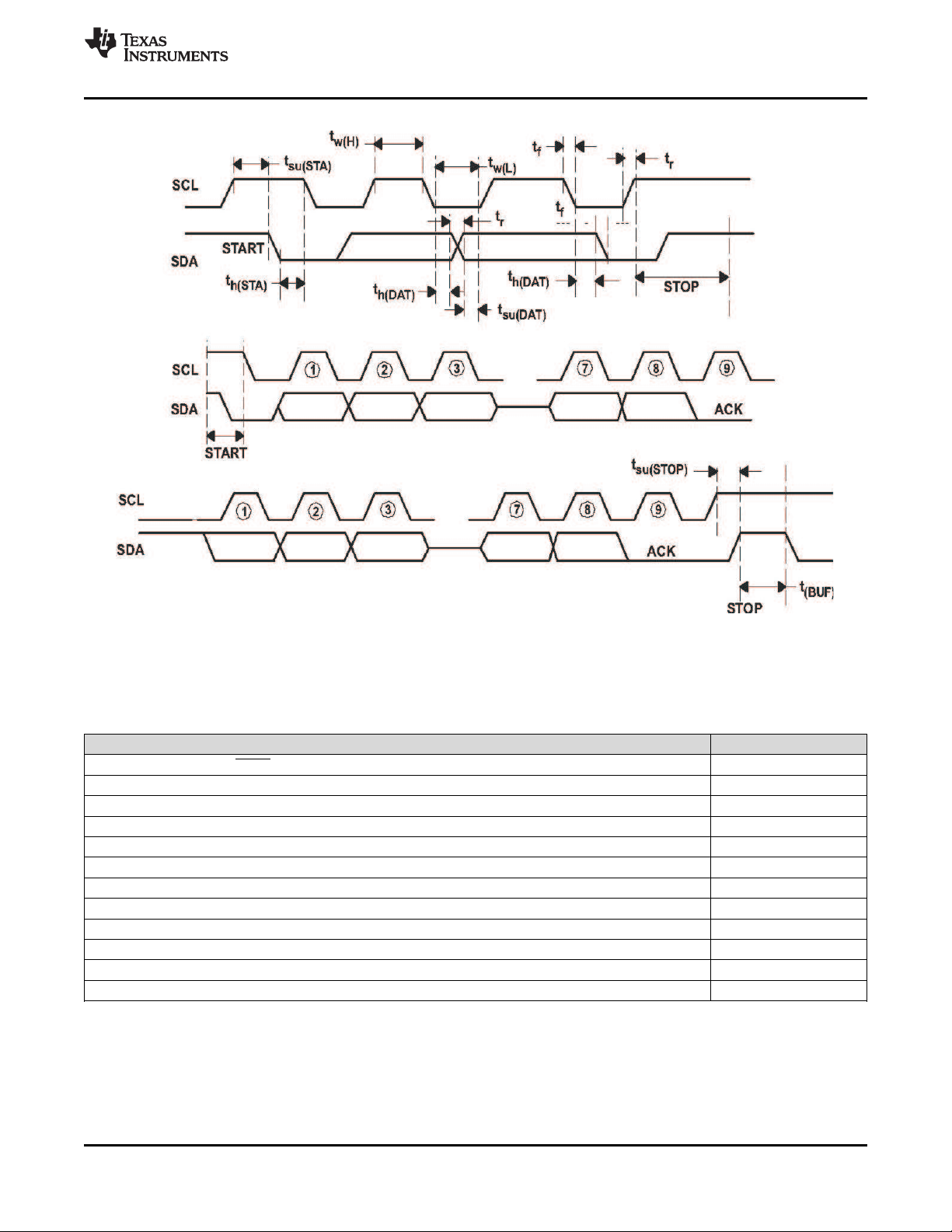
7.6 Timing Requirements
MIN NOM MAX UNIT
ACOK COMPARATOR
V
VCC>VUVLO
ChargeOption() bit [15] = 0 (default), 0.9 1.3 1.7 s
(bq24707 only)
t
ACOK_FALL_DEG
ACOK falling deglitch V
(specified by design) ChargeOption() bit [15] = 0 (default), 0.8 1.2 2 ms
VCC>VUVLO
(bq24707A only)
V
VCC>VUVLO
ChargeOption() bit [15] = 1
PWM DRIVER
t
LOW_HIGH
t
HIGH_LOW
Driver dead time from low side to high side 20 ns
Driver dead time from high side to low side 20 ns
INTERNAL SOFT-START
t
STEP
Soft-start step time In CCM mode, 10-mΩ current-sense 240 μs
resistor
SMBus
t
R
t
F
t
W(H)
t
W(L)
t
SU(STA)
t
H(STA)
t
SU(DAT)
t
H(DAT)
t
SU(STOP)
t
(BUF)
F
S(CL)
SCLK/SDATA rise time 1 μs
SCLK/SDATA fall time 300 ns
SCLK pulse width high 4 50 μs
SCLK pulse width low 4.7 μs
Setup time for START condition 4.7 μs
START condition hold time after which first clock pulse is generated 4 μs
Data setup time 250 ns
Data hold time 300 ns
Setup time for STOP condition 4 µs
Bus free time between START and STOP condition 4.7 μs
Clock frequency 10 100 kHz
HOST COMMUNICATION FAILURE
t
timeout
t
BOOT
t
WDI
t
WDI
t
WDI
SMBus bus release time-out
Deglitch for watchdog reset signal 10 ms
Watchdog time-out period, ChargeOption()
bit [14:13] = 01
Watchdog time-out period, ChargeOption()
bit [14:13] = 10
Watchdog time-out period, ChargeOption()
bit [14:13] = 11
(2)
(2)
(2)
(default)
(1)
(1) Devices participating in a transfer time-out when any clock low exceeds the 25-ms minimum time-out period. Devices that have detected
a time-out condition must reset the communication no later than the 35-ms maximum time-out period. Both a master and a slave must
adhere to the maximum value specified as it incorporates the cumulative stretch limit for both a master (10 ms) and a slave (25 ms).
(2) User can adjust threshold through SMBus ChargeOption() REG0x12.
, V
, V
, V
rising above 2.4 V,
ACDET
rising above 2.4 V,
ACDET
rising above 2.4 V, 10 50
ACDET
25 35 ms
35 44 53 s
70 88 105 s
140 175 210 s
μs
10 Submit Documentation Feedback Copyright © 2010–2015, Texas Instruments Incorporated
Product Folder Links: bq24707 bq24707A
www.ti.com
bq24707,bq24707A
SLUSA78C –JULY 2010–REVISED JULY 2015
Figure 1. SMBus Communication Timing Waveforms
7.7 Typical Characteristics
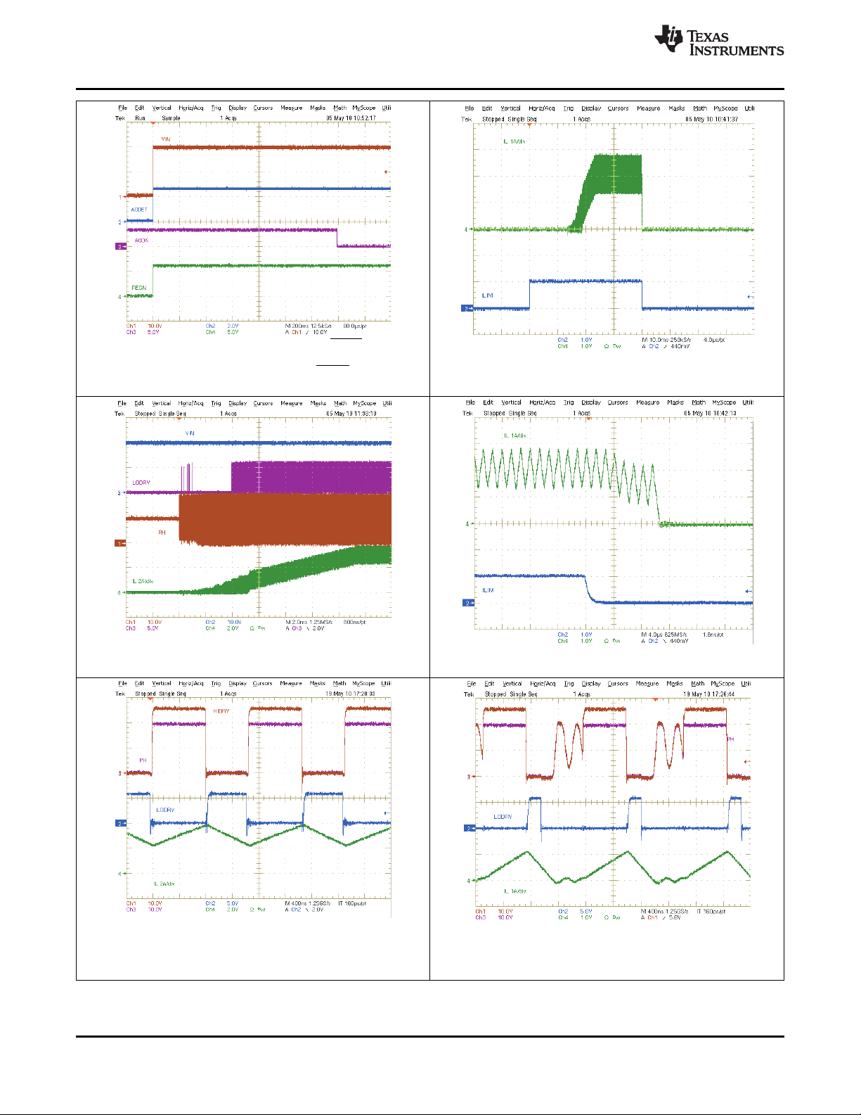
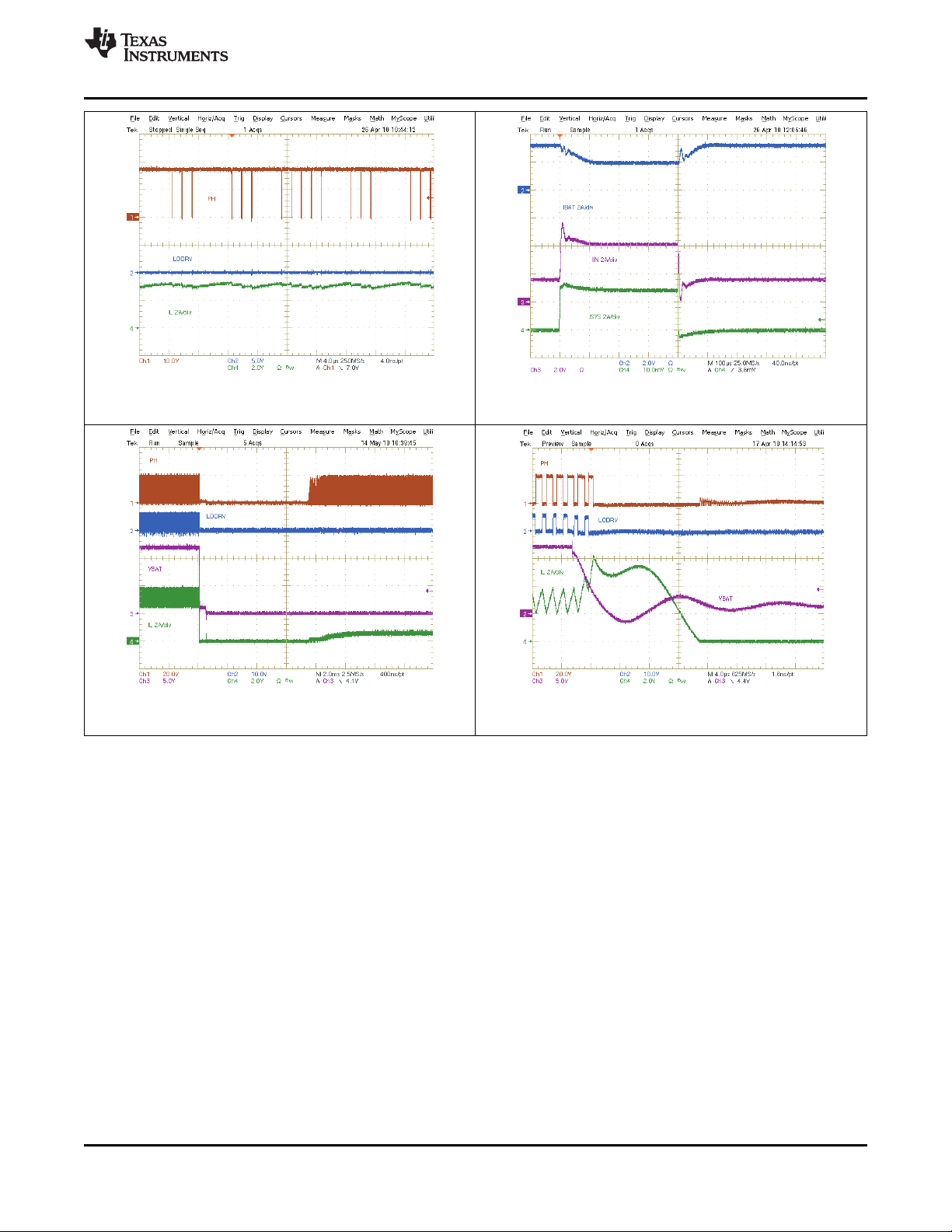
Table 1. Table of Graphs
FIGURE
VCC, ACDET, REGN and ACOK Power Up (bq24707) Figure 2
Charge Enable by ILIM Figure 3
Current Soft-Start Figure 4
Charge Disable by ILIM Figure 5
Continuous Conduction Mode Switching Waveforms Figure 6
Cycle-by-Cycle Synchronous to Nonsynchronous Figure 7
100% Duty and Refresh Pulse Figure 8
System Load Transient (Input DPM) Figure 9
Battery Insertion Figure 18
Battery-to-Ground Short Protection Figure 10
Battery-to-Ground Short Transition Figure 11
Efficiency vs Output Current Figure 19
Copyright © 2010–2015, Texas Instruments Incorporated Submit Documentation Feedback 11
Product Folder Links: bq24707 bq24707A
bq24707,bq24707A
SLUSA78C –JULY 2010–REVISED JULY 2015
CH1: VCC, 10 V/div; CH2: ACDET, 2 V/div; CH3: ACOK, 5 V/div;
CH4: REGN, 5 V/div, 200 ms/div
Figure 2. VCC, ACDET, REGN and ACOK Power Up
(bq24707)
www.ti.com
CH2: ILIM, 1 V/div; CH4: inductor current, 1 A/div, 10 ms/div
Figure 3. Charge Enable by ILIM
CH1: PHASE, 10 V/div; CH2: Vin, 10 V/div; CH3: LODRV, 5 V/div;
CH4: inductor current, 2 A/div, 2 ms/div
Figure 4. Current Soft-Start
CH1: HIDRV, 10 V/div; CH2: LODRV, 5 V/div; CH3: PHASE,
10 V/div; CH4: inductor current, 2 A/div, 400 ns/div
Figure 6. Continuous Conduction Mode Switching
Waveforms
12 Submit Documentation Feedback Copyright © 2010–2015, Texas Instruments Incorporated
Product Folder Links: bq24707 bq24707A
CH2: ILIM, 1 V/div; CH4: inductor current, 1 A/div, 4 µs/div
Figure 5. Charge Disable by ILIM
CH1: HIDRV, 10 V/div; CH2: LODRV, 5 V/div; CH3: PHASE,
10 V/div; CH4: inductor current, 1 A/div, 400 ns/div
Figure 7. Cycle-by-Cycle Synchronous to Nonsynchronous
www.ti.com
bq24707,bq24707A
SLUSA78C –JULY 2010–REVISED JULY 2015
CH1: PHASE, 10 V/div; CH2: LODRV, 5 V/div;
CH4: inductor current, 2 A/div, 4 µs/div
Figure 8. 100% Duty and Refresh Pulse
CH2: battery current, 2 A/div; CH3: adapter current, 2 A/div;
CH4: system load current, 2 A/div, 100 µs/div
Figure 9. System Load Transient (Input DPM)
CH1: PHASE, 20 V/div; CH2: LODRV, 10 V/div; CH3: battery voltage, CH1: PHASE, 20 V/div; CH2: LODRV, 10 V/div; CH3: battery voltage,
5 V/div; CH4: inductor current, 2 A/div, 2 ms/div 5 V/div; CH4: inductor current, 2 A/div, 4 µs/div
Figure 10. Battery-to-Ground Short Protection Figure 11. Battery-to-Ground Short Transition
Copyright © 2010–2015, Texas Instruments Incorporated Submit Documentation Feedback 13
Product Folder Links: bq24707 bq24707A

bq24707,bq24707A
SLUSA78C –JULY 2010–REVISED JULY 2015
www.ti.com
8 Detailed Description
8.1 Overview
The bq24707x device is a 1- to 4-cell battery charge controller with power selection for space-constrained, multichemistry portable applications such as notebooks and detachable ultrabooks. The device supports a wide input
range of input sources from 4.5 V to 24 V, and a 1- to 4-cell battery for a versatile solution.
The bq24707x features Dynamic Power Management (DPM) to limit the input power and avoid AC adapter
overloading. During battery charging, as the system power increases, the charging current will reduce to maintain
total input current below adapter rating.
The SMBus controls input current, charge current and charge voltage registers with high-resolution, highaccuracy regulation limits.
14 Submit Documentation Feedback Copyright © 2010–2015, Texas Instruments Incorporated
Product Folder Links: bq24707 bq24707A
 Loading...