

Texas Instruments bq24702, bq24703 Datasheet
1
2
3
4
5
6
7
8
9
10
11
12
24
23
22
21
20
19
18
17
16
15
14
13
ACDET
ACPRES
ACSEL
BATDEP
SRSET
ACSET
VREF
ENABLE
BATSET
COMP
ACN
ACP
ACDRV
BATDRV
VCC
PWM
VHSP
ALARM
VS
GND
SRP
SRN
IBAT
BATP
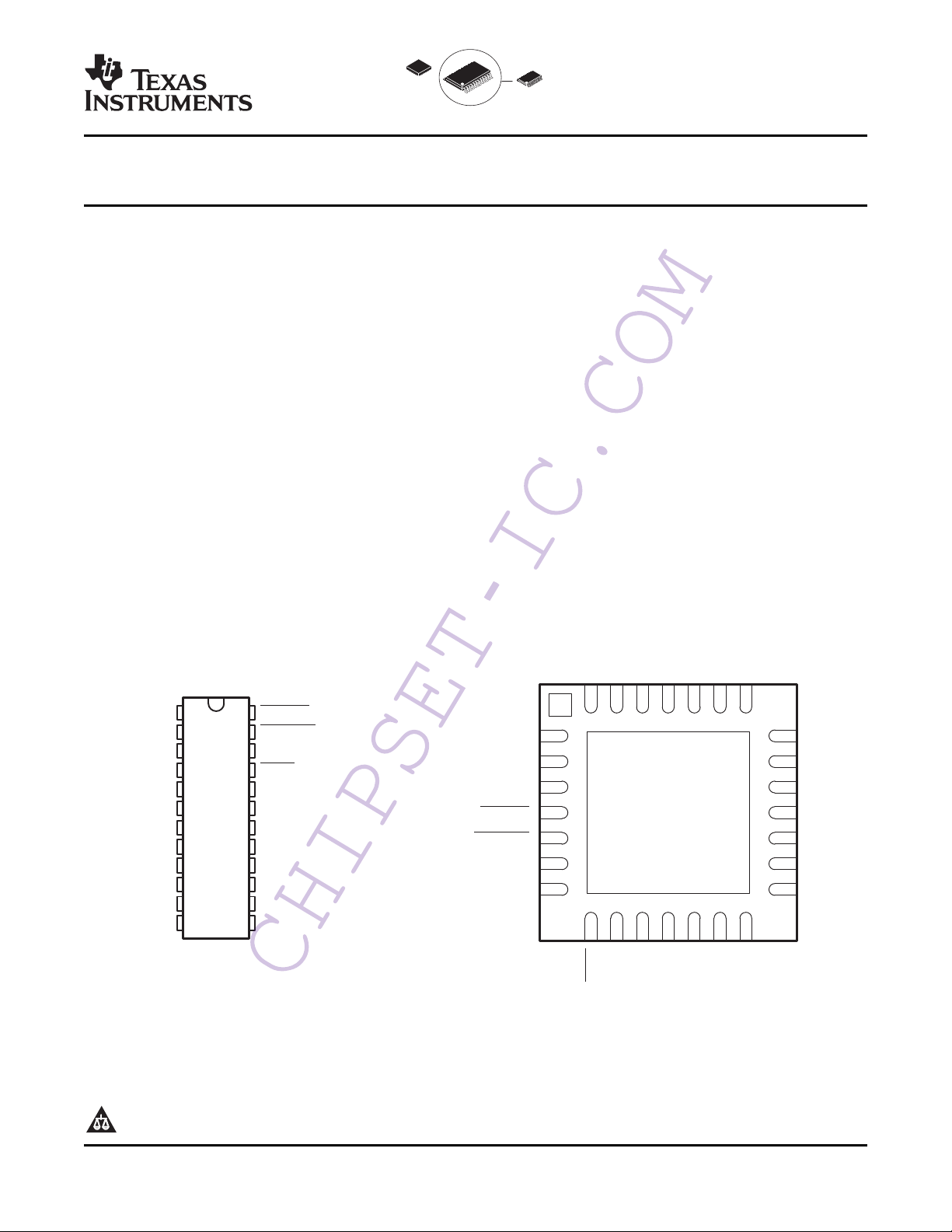
bq24702, bq24703
PW PACKAGE
(TOP VIEW)
8
9
10
11
12
13
14
ACSEL
ACPRES
ACDET
ACDRV
BATDRV
NC
VCC
ACN
ACP
NC
NC
BATP
IBAT
NC
28
27
26
25
24
23
22
1
2
3
4
5
6
7
BATDEP
SRSET
ACSET
VREF
ENABLE
BATSET
COMP
PWM
VHSP
ALARM
VS
GND
SRP
SRN
21
20
19
18
17
16
15
bq24703
RHD PACKAGE
(BOTTOM VIEW)
NC - No internal connection
www.ti.com
MULTICHEMISTRY BATTERY CHARGER CONTROLLER AND
SYSTEM POWER SELECTOR
1
FEATURES
• Dynamic Power Management, DPM Minimizes
Battery Charge Time
• Integrated Selector Supports Battery
Conditioning and Smart Battery Learn Cycle
• Zero Volt Operation
• Selector Feedback Circuit Ensures
Break-Before-Make Transition
• ± 0.4% Charge Voltage Accuracy, Suitable for
Charging Li-Ion Cells
• ± 4% Charge Current Accuracy
• 300-kHz Integrated PWM Controller for
High-Efficiency Buck Regulation
• Depleted Battery Detection and Indication to
Protect Battery From Over Discharge
• 20- μ A Sleep Mode Current for Low Battery
Drain
• 24-Pin TSSOP Package and 5 mm × 5 mm QFN
package (bq24703 only)
bq24702
bq24703
SLUS553E – MAY 2003 – REVISED OCTOBER 2007
DESCRIPTION
The bq24702/bq24703 is a highly integrated battery
charge controller and selector tailored for notebook
and sub-notebook PC applications.
The bq24702/bq24703 uses dynamic power
management (DPM) to minimize battery charge time
by maximizing use of available wall-adapter power.
This is achieved by dynamically adjusting the battery
charge current based on the total system (adapter)
current.
The bq24702/bq24703 uses a fixed frequency, pulse
width modulator (PWM) to accurately control battery
charge current and voltage. Charge current limits can
be programmed from a keyboard controller DAC or
by external resistor dividers from the precision 5-V,
± 0.6%, externally bypassed voltage reference
(VREF), supplied by the bq24702/bq24703.
1
PRODUCTION DATA information is current as of publication date.
Products conform to specifications per the terms of the Texas
Instruments standard warranty. Production processing does not
necessarily include testing of all parameters.
Please be aware that an important notice concerning availability, standard warranty, and use in critical applications of
Texas Instruments semiconductor products and disclaimers thereto appears at the end of this data sheet.
CHIPSET-IC.COM
Copyright © 2003 – 2007, Texas Instruments Incorporated
www.ti.com
0
0.20
0.40
0.60
0.80
1
1.20
1.40
1.60
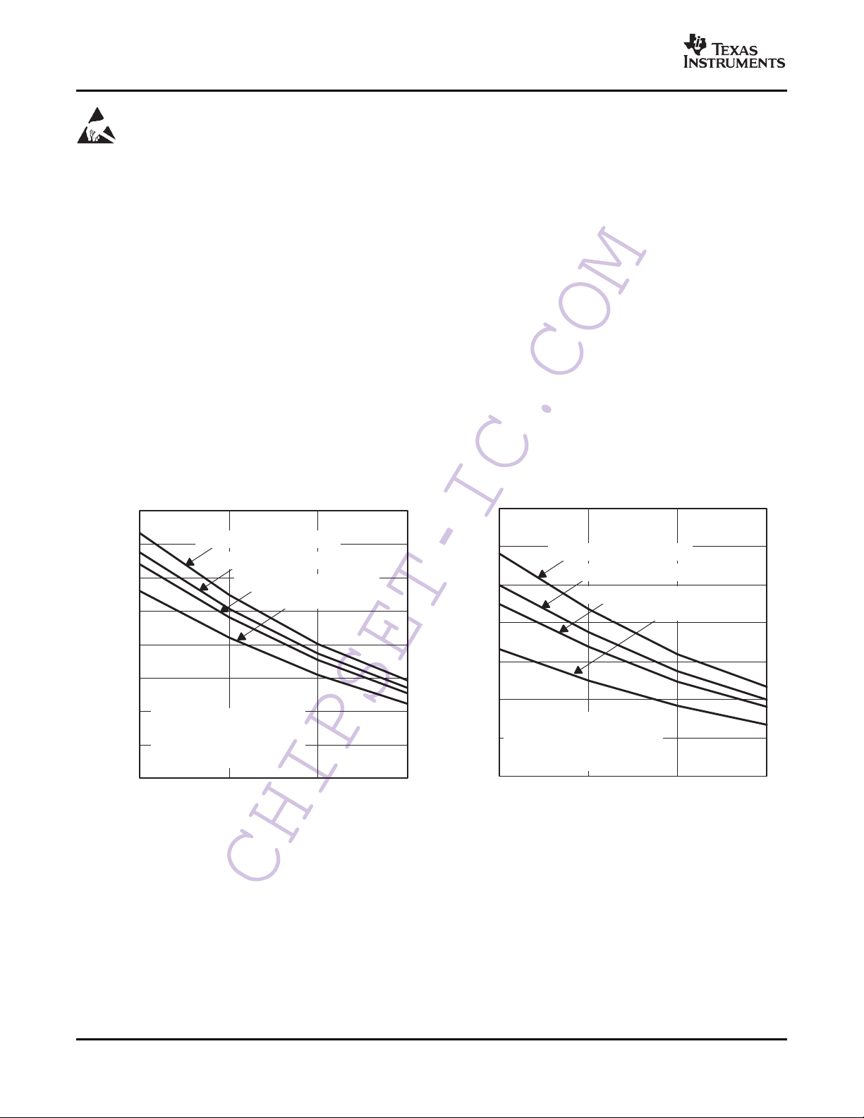
25 50 70 85
MAX Pd (W) @ 500 LFM
MAX Pd (W) @ 250 LFM
MAX Pd (W) @ 150 LFM
MAX Pd (W) @ 0 LFM
θJA = 89.37 C/W @ 0 LFM,
θJA = 77.98 C/W @ 150 LFM,
θJA = 73.93 C/W @ 250 LFM,
θJA = 68.23 C/W @ 500 LFM
Maximum Power Dissipation (High K Board) - W
MAXIMUM POWER DISSIPATION
(HIGH K BOARD)
vs
FREE-AIR TEMPERATURE
TA - Free-Air Temperature - °C
0
0.20
0.40
0.60
0.80
1
1.20
1.40
25 50 70 85
MAX Pd (W) @ 500 LFM
MAX Pd (W) @ 250 LFM
MAX Pd (W) @ 150 LFM
MAX Pd (W) @ 0 LFM
θJA = 150.17 C/W @ 0 LFM,
θJA = 110.95 C/W @ 150 LFM,
θJA = 99.81 C/W @ 250 LFM,
θJA = 86.03 C/W @ 500 LFM
Maximum Power Dissipation (Low K Board) - W
MAXIMUM POWER DISSIPATION
(LOW K BOARD)
vs
FREE-AIR TEMPERATURE
TA - Free-Air Temperature - °C
bq24702
bq24703
SLUS553E – MAY 2003 – REVISED OCTOBER 2007
These devices have limited built-in ESD protection. The leads should be shorted together or the device placed in conductive foam
during storage or handling to prevent electrostatic damage to the MOS gates.
DESCRIPTION (CONTINUED)
The battery voltage limit can be programmed by using the internal 1.196-V, ± 0.5% precision reference, making it
suitable for the critical charging demands of lithium-ion cells. Also, the bq24702/bq24703 provides an option to
override the precision reference and drive the error amplifier either directly from an external reference or from a
resistor divider off the 5 V supplied by the integrated circuit.
The selector function allows the manual selection of the system power source, battery or wall-adapter power.
The bq24702/bq24703 supports battery-conditioning and battery-learn cycles through the ACSEL function. The
ACSEL function allows manual selection of the battery or wall power as the main system power. It also provides
autonomous switching to the remaining source (battery or ac power) should the selected system power source
terminate (refer to Available Options table for the differences between the bq24702 and the bq24703). The
bq24702/bq24703 also provides an alarm function to indicate a depleted battery condition.
The bq24702/bq24703 PWM controller is ideally suited for operation in a buck converter for applications when
the wall-adapter voltage is greater than the battery voltage.
DISSIPATION RATINGS
A. The JEDEC low K (1s) board design used to derive this data was a 3-inch × 3-inch, two layer board with 2 ounce
copper traces on top of the board.
B. The JEDEC high K (1s) board design used to derive this data was a 3-inch × 3-inch, multilayer board with 1 ounce
internal power and ground planes and 2 ounce copper traces on top and bottom of the board.
2 Submit Documentation Feedback Copyright © 2003 – 2007, Texas Instruments Incorporated
CHIPSET-IC.COM
Product Folder Link(s): bq24702 bq24703

www.ti.com
SLUS553E – MAY 2003 – REVISED OCTOBER 2007
AVAILABLE OPTIONS
CONDITION
20 ° C ≤ TJ≤ 125 ° C
BATTERY AS POWER SOURCE
Battery removal Automatically selects ac + alarm Automatically selects ac + alarm
Battery reinserted Selection based on selector inputs Adapter latched until adapter is removed or ac select toggles.
AC AS POWER SOURCE
AC removal Automatically selects battery Automatically selects battery
AC reinserted Selection based on selector inputs Selection based on selector inputs
DEPLETED BATTERY CONDITION
Battery as power source Sends ALARM signal Automatically selects ac Sends ALARM signal
AC as power source Sends ALARM signal Sends ALARM signal
ALARM SIGNAL ACTIVE
Depleted battery condition Depleted battery condition
When selector input is not equal to selector
output (single pulse alarm)
bq24702PW bq24703RHD
SELECTOR OPERATION
bq24702
bq24703
ABSOLUTE MAXIMUM RATINGS
over operating free-air temperature range (unless otherwise noted)
V
CC
T
J
T
stg
(1) Stresses beyond those listed under absolute maximum ratings may cause permanent damage to the device. These are stress ratings
(2) All voltages are with respect to ground. Currents are positive into and negative out of the specified terminals. Consult the Packaging
Supply voltage range – 0.3 to 30 V
Battery voltage range: SRP, SRN – 0.3 to 30 V
Input voltage: ACN, ACP – 0.3 to 30 V
Virtual junction temperature range – 40 to 125 ° C
Maximum source/sink current VHSP 50 mA
Maximum ramp rate for V
Maximum sink current ACPRES, COMP, ALARM 2.5 mA
Maximum ramp rate for V
Maximum source/sink current BATDRV 10 mA
Maximum source/sink current ACDRV 10 mA
Maximum source/sink current PWM 50 mA
Maximum source/sink current pulsed ACDRV, (10- μ s rise time, 10- μ s fall time, 1-ms
pulse width, single pulse)
Maximum source current VREF 30 mA
Maximum source current SRP 100 mA
Maximum difference voltage SRP – SRN 30 V
Storage temperature range – 65 to 150 ° C
only, and functional operation of the device at these or any other conditions beyond those indicated under recommended operating
conditions is not implied. Exposure to absolute-maximum-rated conditions for extended periods may affect device reliability.
section of the data book for thermal limitations and considerations of the package.
CC
(BAT)
(1) (2)
VALUE UNIT
10 V/ μ s
10 V/ μ s
50 mA
CHIPSET-IC.COM
Copyright © 2003 – 2007, Texas Instruments Incorporated Submit Documentation Feedback 3
Product Folder Link(s): bq24702 bq24703

www.ti.com
bq24702
bq24703
SLUS553E – MAY 2003 – REVISED OCTOBER 2007
RECOMMENDED OPERATING CONDITIONS
(T
= T
A
Supply voltage, (VCC) V
Negative ac current sense, (ACN) 7 28 V
Positive ac current sense, (ACP) 7 28 V
Negative battery current sense, (SRN) 5 28 V
Positive battery current sense, (SRP) 5 28 V
AC or adapter power detection (ACDET) 0 5 V
AC power indicator (ACPRES) 0 5 V
AC adapter power select (ACSEL) 0 5 V
Depleted battery level (BATDEP) 0 5 V
Battery charge current programming voltage (SRSET) 0 2.5 V
Charge enable (ENABLE) 0 5 V
External override to an internal 0.5% precision reference (BATSET) 0 2.5 V
Inverting input to the PWM comparator (COMP) 0 5 V
Battery charge regulation voltage measurement input to the battery — voltage gmamplifier (BATP) 0 5 V
Battery current differential amplifier output (IBAT) 0 5 V
System load voltage input pin (VS) 0 2.5 V
Depleted battery alarm output (ALARM) 0 5 V
Gate drive output ( PWM) VHSP VCC V
Battery power source select output ( BATDRV) 0 28 V
AC or adapter power source selection output ( ACDRV) VHSP VCC V
ACSET 0 2.5 V
Operating free-air temperature, T
) all voltages relative to V
OPR
SS
Analog and PWM operation 7 28
Selector operation 4.5 28
A
MIN MAX UNIT
-40 85 ° C
CHIPSET-IC.COM
4 Submit Documentation Feedback Copyright © 2003 – 2007, Texas Instruments Incorporated
Product Folder Link(s): bq24702 bq24703

www.ti.com
ELECTRICAL CHARACTERISTICS
– 40 ° C ≤ TJ≤ 125 ° C, 7 V
QUIESCENT CURRENT
I
DD(OP)
I
DD(SLEEP)
LOGIC INTERFACE DC CHARACTERISTICS
V
OL
V
IL
V
IH
I
(SINK1)
I
(SINK2)
PWM OSCILLATOR
f
OSC(PWM)
V
(RAMP)
V
IK(COMP)
I
S(COMP)
LEAKAGE CURRENT
I
L( ACDET)
I
L(SRSET)
I
L(ACSET)
I
L(BATDEP)
I
L(VS)
I
L(ALARM)
I
L(ACSEL)
I
L(ENABLE)
I
L(ACPRES)
I
L(BATP)
I
L(BATSET)
Total chip operating current ACPRES = High, EN = 0 1 1.6 6 mA
Total battery sleep current, ac not present ACPRES = Low 22 28 μ A
Low-level output voltage (ACPRES, ALARM) IOL= 1 mA 0.4 V
Low-level input voltage (ACSEL, ENABLE) 0.6 V
High-level input voltage (ACSEL, ENABLE) 1.8 V
Sink current (ACPRES) V
Sink current (ALARM) V
Oscillator frequency kHz
Maximum duty cycle 100%
Input voltage for maximum dc (COMP) 3.8 V
Minimum duty cycle 0%
Input voltage for minimum dc (COMP) 0.8 V
Oscillator ramp voltage (peak-to-peak) 1.85 2.15 2.30
Internal input clamp voltage
(tracks COMP voltage for maximum dc)
Internal source current (COMP) Error amplifier = OFF, V
Leakage current, ACDET V
Leakage current, SRSET V
Leakage current, ACSET V
Leakage current, BATDEP V
Leakage current, VS V
Leakage current, ALARM V
Leakage current, ACSEL V
Leakage current, ENABLE V
Leakage current, ACPRES V
Leakage current, BATP V
Leakage current, BATSET V
SLUS553E – MAY 2003 – REVISED OCTOBER 2007
≤ V
DC
≤ 28 V
CC
, all voltages relative to V
DC
(unless otherwise specified)
SS
PARAMETER TEST CONDITIONS MIN TYP MAX UNIT
= 0.4 1.5 2 2.5 mA
OL
= 0.4 1.5 2 2.5 mA
OL
0 ° C ≤ TJ≤ 85 ° C 280 300 340
– 40 ° C ≤ TJ≤ 125 ° C 240 300 350
3.8 4.5
= 1 V 70 110 140 μ A
(COMP)
= 5 V 0.2 μ A
(ACDET)
= 2.5 V 0.2 μ A
(SRSET)
= 2.5 V 0.2 μ A
(ACSET)
(BATDEP)
(VS)
(ALARM)
(ACSEL)
(ENABLE)
(ACPRES)
(BATP)
(BATSET)
= 5 V 0.2 μ A
= 5 V 0.2 μ A
= 5 V 0.2 μ A
= 5 V 0.2 μ A
= 5 V 0.2 μ A
= 5 V 0.2 μ A
= 5 V 0.2 μ A
= 2.5 V 0.2 μ A
bq24702
bq24703
CHIPSET-IC.COM
Copyright © 2003 – 2007, Texas Instruments Incorporated Submit Documentation Feedback 5
Product Folder Link(s): bq24702 bq24703

www.ti.com
I
BAT
+
SRSET
R
SENSE
1
A
V
Dc +
SRSET
A
V
, Totalaccuracy in % +
(
Dm* Dc
)
Dc
100,I
(SRP)
* I
(SRN)
+ 0
bq24702
bq24703
SLUS553E – MAY 2003 – REVISED OCTOBER 2007
ELECTRICAL CHARACTERISTICS (Continued)
– 40 ° C ≤ TJ≤ 125 ° C, 7 V
BATTERY CURRENT-SENSE AMPLIFIER
g
m
CMRR Common-mode rejection ratio See
V
ICR
I
(SINK)
I
IB
V
(SET)
A
V
(1) Specified by design. Not production tested.
(2) I
(SRP)
example: If (V
Transconductance gain 75 120 175 mA/V
Common-mode input (SRP, SRN) voltage
range
Sink current (COMP) COMP = 1 V, (SRP – SRN) = 10 mV 0.5 1.5 2.5 mA
Input bias current (SRP)
Input bias current accuracy (I
Battery current programming voltage (SRSET) 0 2.5 V
Battery current set gain 24 25 26 V/V
Total battery current-sense mid-scale accuracy
Total battery current-sense full-scale accuracy
= I
= (V
(SRN)
(SRSET)
≤ V
CC
/ 50 k Ω ) + ((V
≤ 28 V
DC
PARAMETER TEST CONDITIONS MIN TYP MAX UNIT
(SRSET)
= 2.5 V) , (V
, all voltages relative to V
DC
(2)
– I
SRP
SRN
- V
(SRP)
- V
(SRP)
(SRN)
= 100 mV) Then I
(SRN)
) – 3 0 3
(unless otherwise specified)
SS
(1)
VCC = SRN, SRP + 2 V 5 30 V
V
= 16 V, (SRP – SRN) = 100 mV,
(SRP)
SRSET = 2.5 V, VCC = 28
(SRP - SRN) = 100 mV, SRSET= 2.5 V,
VCC = 28 V, 0 ≤ TJ≤ 125 ° C
0.65 V ≤ SRSET ≤ 2.5 V,
8 V ≤ SRN ≤ 16 V
SRSET = 1.25 V, TJ= 25 ° C
SRSET = 1.25 V
SRSET = 2.5 V, TJ= 25 ° C
SRSET = 2.5 V
/ 3 k Ω )
(SRP)
(3)
(4)
(4)
= I
= 83 A
(SRN)
(4)
(4)
70 85 110
– 5% 5%
– 6% 6%
– 3% 3%
– 4% 4%
90 dB
μ A
(3)
(4) Total battery-current set is based on the measured value of (SRP – SRN) = Δ m, and the calculated value of (SRP – SRN) = Δ C, using the
measured gain, AV.
CHIPSET-IC.COM
6 Submit Documentation Feedback Copyright © 2003 – 2007, Texas Instruments Incorporated
Product Folder Link(s): bq24702 bq24703

www.ti.com
ELECTRICAL CHARACTERISTICS (Continued)
I
AC
+
ACSET
R
SENSE
1
A
V
Dc +
ACSET
A
V
, Totalaccuracy in % +
(
Dm* Dc
)
Dc
100,I
(ACP)
* I
(ACN)
+ 0
– 40 ° C ≤ TJ≤ 125 ° C, 7 V
PARAMETER TEST CONDITIONS MIN TYP MAX UNIT
ADAPTER CURRENT-SENSE AMPLIFIER
g
m
CMRR Common-mode rejection ratio See
V
I
(SINK)
I
IB
V
A
BATTERY VOLTAGE ERROR AMPLIFIER
g
m
CMRR Common-mode rejection ratio See
V
V
I
(SINK)
V
Transconductance gain 75 130 175 mA/V
Common-mode input voltage range (ACP) 7 V
ICR
Sink current (COMP) COMP = 1 V, (ACP – ACN) = 10 mV 0.5 1.5 2.5 mA
Input bias current (ACP, ACN) 40 50 65
Input bias current accuracy ratio ACP = ACN = 28 V, VCC = 28 V,
(I
, I
(ACP)
(ACN)
AC current programming voltage (ACSET) 0 2.5 V
(SET)
AC current set gain 0.65 V ≤ ACSET ≤ 2.5 V, 12 V ≤ ACP ≤ 20 V
V
Total ac current-sense mid-scale accuracy
Total ac current-sense full-scale accuracy ACSET = 2.5 V, TJ= 25 ° C
Transconductance gain 75 135 175 mA/V
BATSET common-mode input voltage
ICR
range
Internal reference override input threshold
IT
voltage
Sink current COMP 0.5 1.5 2.5 mA
Error-amplifier precision reference voltage TJ= 0 ° C to 85 ° C 1.183 1.196 1.203 V
(FB)
≤ V
DC
) ACSET = 2.5 V, 0 ≤ TJ≤ 125 ° C
≤ 28 V
CC
, all voltages relative to VSS, (unless otherwise specified)
DC
SLUS553E – MAY 2003 – REVISED OCTOBER 2007
(1)
ACP = ACN = 28 V, VCC = 28 V, ACSET = 2.5
V
– 3 0 3
(1)
ACSET = 1.25 V, TJ= 25 ° C
ACSET = 1.25 V
ACSET = 2.5 V
(1)
COMP = 1 V, (BATP – BATSET) = 10 mV,
BATSET = 1.25 V
TJ= 25 ° C 1.190 1.196 1.202
TJ= – 40 ° C to 125 ° C 1.178 1.196 1.204
(2)
(2)
(2)
(2)
24.5 25.3 26.5 V/V
– 5% 5%
– 6% 6%
– 3.5% 3.5%
– 4% 4%
1 2.5 V
0.20 0.25 0.35 V
bq24702
bq24703
90 dB
CC
90 dB
V
A
(1) Calculation of the ac current:
(2) Total ac-current set accuracy is based on the measured value of (ACP-ACN) = Δ c, using the measured gain, A
V.
CHIPSET-IC.COM
Copyright © 2003 – 2007, Texas Instruments Incorporated Submit Documentation Feedback 7
Product Folder Link(s): bq24702 bq24703

www.ti.com
G
TR
+
V
IBAT
(
SRP* SRN
)
bq24702
bq24703
SLUS553E – MAY 2003 – REVISED OCTOBER 2007
ELECTRICAL CHARACTERISTICS (Continued)
– 40 ° C ≤ TJ≤ 125 ° C, 7 V
PARAMETER TEST CONDITIONS MIN TYP MAX UNIT
BATTERY CURRENT OUTPUT AMPLIFIER
G
V
CM Common-mode input range (SRP) 5 28 V
V
T)
I
5-V VOLTAGE REFERENCE
V
HALF SUPPLY REGULATOR
V
Transfer gain (SRP – SRN) = 5 mV
(TR)
Battery current readback output (SRP – SRN) = 5 mV, SRP = 12 V,
I(BAT)
voltage (IBAT) V
Line rejection voltage TJ= 25 ° C 10 mV/V
Battery current output voltage
O(IBA
range (IBAT)
Output source current (IBAT) (SRP – SRN) = 100 mV 5 7.1 9.4 mA
S(O)
Total battery current readback
full-scale accuracy
Output voltage (VREF) TJ= 25 ° C 4.985 5 5.013 V
ref
Line regulation I
Load regulation 1 mA ≤ I
Short circuit current 8 20 30 mA
5V REF output capacitor Capacitance 2.2 10 μ F
Output capacitor equivalent
resistor
Voltage regulation V
(HSP)
≤ V
DC
≤ 28 V
CC
, all voltages relative to V
DC
(1)
= 18 V, TJ= 25 ° C
CC
(SRP – SRN) = 50 mV, TJ= 25 ° C
(SRP – SRN) = 50 mV,
0 ° C ≤ TJ≤ 85 ° C
(SRP – SRN) = 100 mV,
TJ= 25 ° C
(SRP – SRN) = 100 mV,
0 ° C < TJ< 85 ° C
TJ= 0 ° C to 85 ° C 4.946 5 5.013
TJ= 40 ° C to 85 ° C 4.946 5 5.03 V
TJ= – 40 ° C to 125 ° C 4.926 5 5.03 V
LOAD
ESR 5 1000 m Ω
I
(SINK)
I
(SINK)
(1)
= 5 mA 0.1 0.37 mV/V
≤ 5 mA 1.1 4 mV/mA
LOAD
= 20 mA, V
= 1 mA, V
= 18 V V
CC
= 7 V 1.5
CC
(unless otherwise specified)
SS
20 V/V
100 mV
0 2.5 V
(1)
– 3% 2.4%
– 20% 20%
– 1.5% 1.2%
– 6% 8.5%
CC
– 11 V
CC
– 10.2 V
– 8.5
CC
(1) Battery readback transfer gain
CHIPSET-IC.COM
8 Submit Documentation Feedback Copyright © 2003 – 2007, Texas Instruments Incorporated
Product Folder Link(s): bq24702 bq24703

www.ti.com
ELECTRICAL CHARACTERISTICS (Continued)
V
IBATc
+
(
SRP* SRN) GTR Total Accuracy in % +
V
IBATm
* V
IBATc
V
IBATm
100
– 40 ° C ≤ TJ≤ 125 ° C, 7 V
PARAMETER TEST CONDITIONS MIN TYP MAX UNIT
MOSFET GATE DRIVE
AC driver R
AC driver R
Battery driver R
Battery driver R
t
da
t
db
V
OH
V
OL
SELECTOR
V
(ACPRES)
V
IT(ACPRES)
t
d(ACPRES)
V
(BATDEP)
V
(NOBAT)
t
(BATSEL)
t
(ACSEL)
V
(VS)
V
IT(VS)
ZERO VOLT OPERATION
r
DS(on)
(1) Total battery current readback accuracy is based on the measured value of V
using the measured value of the transfer gain, GTR.
Time delay from ac driver off to
battery driver on
Time delay from battery driver off to
ac driver on
PWM driver high-level output
voltage
PWM driver R
PWM driver low-level output voltage V
PWM driver R
AC presence detect voltage V
AC presence hysteresis 1%
Deglitch delay for adapter insertion 100 μ s
Battery depletion ALARM trip
voltage
No battery detect, switch to ACDRV bq24702 only
Battery select time (ACSEL low to VS < BATP, 50% threshold, ACSEL
BATDRV low) 2.4 V ↓ 0.2 V
AC select time (ACSEL high to
ACDRV low)
VS voltage to enable BATDRV BATP = 1 V 0.98 1 1.02 V
VS voltage hysteresis VS > BATP 20 35 85 mV
Static drain source on-state
resistance
Zero volt operation threshold V
≤ V
DC
CC
high V
DS(on)
low V
DS(on)
DS(on)
DS(on)
high 7 14 Ω
DS(on)
low 5 8.5 Ω
DS(on)
(2)
≤ 28 V
, all voltages relative to V
DC
high V
low V
SS
CC
CC
CC
CC
= 18 V, I
= 18 V, I
= 18 V, I
= 18 V, I
= 1 mA 85 150 Ω
( ACDRV)
= 1 mA 55 110 Ω
( ACDRV)
( BATDRV)
( BATDRV)
= 1 mA 315 600 Ω
= 1 mA 70 115 Ω
ACSEL 2.4 V ^ 0.2 V 1.2 2 μ s
ACSEL 0.2 V $ 2.4 V 2.4 3.3 μ s
IO= – 10 mA, VCC = 18 V V
IO= – 50 mA, VCC = 18 V V
IO= 10 mA, VCC = 18 V V
IO= 50 mA, VCC = 18 V V
– 40 ° C to 85 ° C 1.208 1.246 1.285
(1)
See
– 40 ° C to 85 ° C 1.208 1.246 1.285
(1)
– 40 ° C to 85 ° C 0.880 1 1.118
ACSEL 0.2 V ↑ 2.4 V 1 2.5 5 μ s
V
= 7 V, TJ= 125 ° C, IO= 100 mA 5.3 8.7 Ω
CC
BATDEP increasing 0.743 0.794 0.840
BATDEP decreasing 0.570 0.62 0.656
(unless otherwise specified)
, V
IBAT
SLUS553E – MAY 2003 – REVISED OCTOBER 2007
CC
CC
– 0.18 V
– 1.2 V
– 0.09
CC
– 0.8
CC
+0.1 V
HSP
+0.6 V
HSP
1.194 1.246 1.286
1.194 1.246 1.286
0.869 1 1.144 V
1 2.5 3.5 μ s
, and the calculated value of V
IBATm
bq24702
bq24703
V
+0.4
HSP
+1.2
HSP
V
, V
IBAT
,
IBATc
(2) See Table 1 to determine the logic operation of the bq24702 and the bq24703.
Copyright © 2003 – 2007, Texas Instruments Incorporated Submit Documentation Feedback 9
CHIPSET-IC.COM
Product Folder Link(s): bq24702 bq24703
www.ti.com
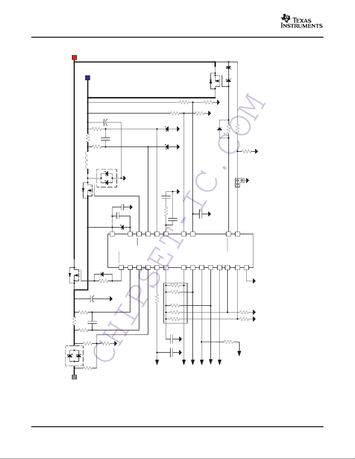
R6
R11
Open
R12
Note1
R14
0.025
R13
R15
C3
C12
35V
U2
SI4435DY
R18
D2
BAS16
ACDRV24
ACN11
12 ACP
1
ACDET
22VCC
20
VHSP
D3
13 V
21
SRP
C6
16V
C7
35 V
PWM
L1
U3
SI4435DY R20
SRN
D5
Note 1
D6
Note 1
R22
R23
Note1
R24
R25
Note1
16
15
BATDEP
BATP
4
13
R16
C5
C4
150pF
10COMP
D1
MBRD640CTT4
D4
MBRD640CTT4
C11
35 V
R21
Note1
R19
Note1
C8
U4
SI4435DY
D9 BAS16
R26 100K
BATDRV
23
SYSTEM
R27
R28
Note1
Battery Plus
VS 18
AC Adapter
VREF7
ENABLE
ACSEL3
8
19 ALARM
ACPRES
2
C1
ENABLE
ACSEL
ALARM
ACPRES
5
6
SRSET
ACSET
R2
R10
Note1
R8
Note1
C10
180pF
14 IBAT
C13
1 nF
IBAT
R29
17
GND
9BATSET BATSET
100 kΩ
100 Ω
1µ
F
100 Ω
10Ω
33µ
H
4.7µ
F
1µ
F
0.025 Ω
22µ
F
100 Ω
4.7µ
F
604 kΩ
Connect to GND
to Disable
100 kΩ
30 kΩ
4.7µ
F
Note 1: R8 Sets AC Adapter Current Limit
R10 Sets Charge Current
R12 Sets AC ADAPTER Current Limit
R23 Sets the Battery Depleted Threshold
R25 Sets the Charge Regulation Voltage
R28 Sets System Break Before Make
R19 = R21, Sets Zero Volt Charge Current
bq24703
bq24702
Note1
604 kΩ
604 kΩ
Note1
Note1
C11 Optional, See Application Notes
C12 For Value, See Application Notes
C8 Value Depends on R21 and R19, See Application Notes
D5, D6 Refer to the Application Section
PROCESSOR’S
POWER SUPPLY
bq24702
bq24703
SLUS553E – MAY 2003 – REVISED OCTOBER 2007
APPLICATION DIAGRAM
10 Submit Documentation Feedback Copyright © 2003 – 2007, Texas Instruments Incorporated
CHIPSET-IC.COM
Product Folder Link(s): bq24702 bq24703
www.ti.com
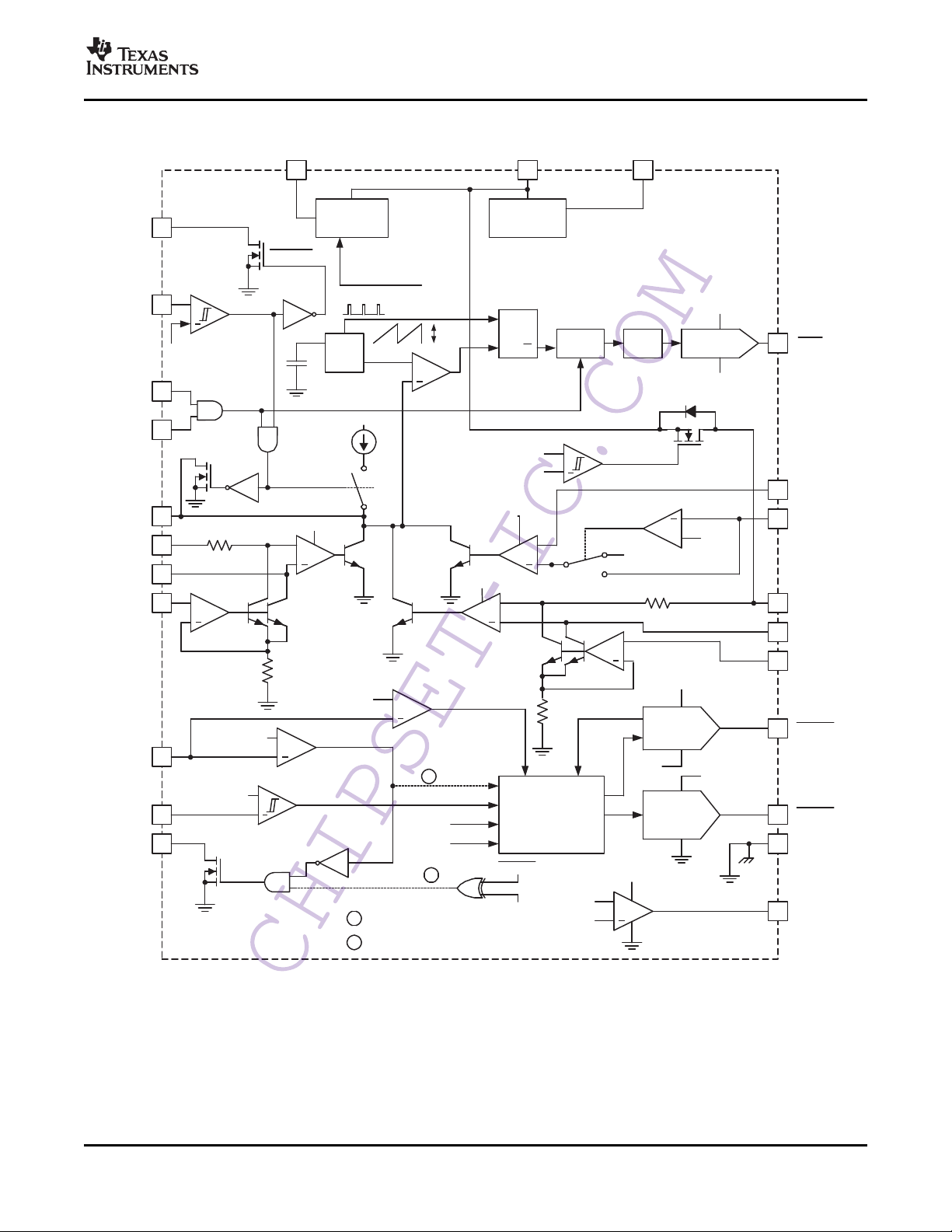
UDG-00137
20
VHSP
VHSP
REGULATOR
22
VCC
7
VREF
VOLTAGE
REFERENCE
VREF
ACPRES
2ACPRES
+
1ACDET
ACPRES
HYST
LEVEL
SHIFT
S Q
QR
PWM
LOGIC
OSC
21
HIGH-SIDE
DRIVE
300 kHz
+
3ACSEL
8ENABLE
VCC
VHSP
10COMP
5 V
100µA
+
+
5 V
SRN
+
2 k
Ω
12ACP
11ACN
+
6ACSET
25
k
Ω
VCC
ac
CURRENT
ERROR
AMPLIFIER
BATTERY
CURRENT
ERROR
AMPLIFIER
BATTERY
VOLTAGE
ERROR
AMPLIFIER
+
13
PWM
BATP
9 BATSET
16 SRP
2 k
Ω
15 SRN
5 SRSET
25
k
Ω
0.25 V
BATTERY
SELECT
DRIVE
ADAPTER
SELECT
DRIVE
+
24
VCC
VHSP
VCC
23 BATDRV
BATTERY SELECT
LOGIC
AND
ANTI-CROSS
CONDUCT
+
NO BATTERY
COMPARATOR
17 GND
+
A=20
VCC
14 IBAT
SRP
SRN
ACSEL
ACPRES
+
SWITCH TO
BATTERY
4BATDEP
+
DEPLETED
BATTERY
COMPARATOR
BATP
18VS
2
2
1
1
ACDRV
ACDRV
ACSEL
bq24702 ONLY
bq24703 ONLY
19ALARM
2 V
+
BATDA
VTBD
Zero Volt
Charging
V
ACPRES
V
FB
0.8 x V
NOBAT
V
BATDEP
bq24702
bq24703
SLUS553E – MAY 2003 – REVISED OCTOBER 2007
BLOCK DIAGRAM
CHIPSET-IC.COM
Copyright © 2003 – 2007, Texas Instruments Incorporated Submit Documentation Feedback 11
Product Folder Link(s): bq24702 bq24703

www.ti.com
bq24702
bq24703
SLUS553E – MAY 2003 – REVISED OCTOBER 2007
Table 1. TERMINAL FUNCTIONS
TERMINAL
NAME
ACDET 1 26 I AC or adapter power detection
ACDRV 24 25 O AC or adapter power source selection output
ACN 11 8 I Negative differential input
ACP 12 9 I Positive differential input
ACPRES 2 27 O AC power indicator
ACSEL 3 28 I AC adapter power select
ACSET 6 3 I Adapter current programming voltage
ALARM 19 19 O Alarm output
BATDEP 4 1 I Depleted battery level
BATDRV 23 24 O Battery power source select output
BATP 13 12 I Battery charge regulation voltage measurement input to the battery-voltage gmamplifier
BATSET 9 6 I External override to an internal precision reference
COMP 10 7 O Inverting input to the PWM comparator
ENABLE 8 5 I Charge enable
GND 17 17 O Supply return and ground reference
IBAT 14 13 O Battery current differential amplifier output
PWM 21 21 O Gate drive output
SRN 15 15 I Negative differential battery current sense amplifier input
SRP 16 16 I/O Positive differential battery current sense amplifier input
SRSET 5 2 I Battery charge current programming voltage
VCC 22 22 I Operational supply voltage
VHSP 20 20 O Voltage source to drive gates of the external MOSFETs
VREF 7 4 O Precision 5-V reference
VS 18 18 I System (load) voltage input pin
bq24702 bq24703
(PW) (QFN)
I/O DESCRIPTION
PIN ASSIGNMENTS
ACDET: AC or adapter power detection. This input pin is used to determine the presence of the ac adapter.
When the voltage level on the ACDET pin is less than V
PWM control is disabled, the BATDRV is driven low, and the ACDRV is driven high. This feature can be used to
automatically select battery as the system power source.
ACDRV: AC or adapter power source select output. This pin drives an external P-channel MOSFET used to
switch to the ac wall-adapter as the system power source. When the ACSEL pin is high while the voltage on the
ACDET pin is greater than V
when the ACDET is less than V
, the output ACDRV pin is driven low (V
ACPRES
.
ACPRES
ACN, ACP: Negative and positive differential inputs, respectively for ac-to-dc adapter current sense resistor.
ACPRES: This open-drain output pin is used to indicate the presence of ac power. A logic high indicates there is
a valid ac input. A low indicates the loss of ac power. ACPRES is high when the voltage level on the ACDET pin
is greater than V
.
ACPRES
CHIPSET-IC.COM
ACSEL: AC adapter power select. This input selects either the ac adapter or the battery as the power source. A
logic high selects ac power, while a logic low selects the battery.
ACSET: Adapter current programming voltage. This input sets the system current level at which dynamic power
management occurs. Adapter currents above this programmed level activate the dynamic power management
and proportionally reduce the available power to the battery.
12 Submit Documentation Feedback Copyright © 2003 – 2007, Texas Instruments Incorporated
Product Folder Link(s): bq24702 bq24703
, the bq24702/bq24703 is in sleep mode, the
ACPRES
). This pin is driven high (V
HSP
)
CC
 Loading...