

Texas Instruments BQ24650 Datasheet
VCC
REGN
BTST
HIDRV
PH
LODRV
GND
SRP
SRN
VFB
VREF
MPPSET
TS
TERM_EN
STAT1
STAT2
Q2
L
C9
R
SR
BQ24650
C6
Q1
C1
Solar Cell
Half Panel
C8
Battery Pack
C7
C4
C3
C2
C10
R2
R1
R3
R4
R9
R10
Pack
Thermistor
R7
R8
VIN
R5
R6
CE
VIN
D3
D4
D2
C5
D1
Q3
Thermal
Pad
Product
Folder
Order
Now
Technical
Documents
Tools &
Software
Support &
Community
BQ24650
SLUSA75B –JULY 2010–REVISED JANUARY 2020
BQ24650 Stand-Alone Synchronous Buck Battery Charge Controller for Solar Power
With Maximum Power Point Tracking
1 Features
1
• Maximum Power Point Tracking (MPPT) capability
by input Voltage regulation
• Programmable MPPT setting
• 5-V to 28-V Input solar panel
• 600-kHz NMOS-NMOS Synchronous buck
controller
• Resistor programmable float voltage
• Accommodates Li-Ion/Polymer, LiFePO4, lead
acid chemistries
• Accuracy
– ±0.5% Charge voltage regulation
– ±3% Charge current regulation
– ±0.6% Input voltage regulation
• High Integration
– Internal loop compensation
– Internal digital soft start
• Safety
– Input overvoltage protection
– Battery temperature-sensing
– Battery absent detection
– Thermal shutdown
• Charge status outputs for LED or host processor
• Charge enable on MPPSET pin
• Automatic sleep mode for low power consumption
– < 15-μA OFF-state battery discharge current
• Small 3.5 × 3.5 mm216-pin QFN package
2 Applications
• Solar-powered applications
• Remote monitoring stations
• Portable handheld instruments
• 12-V to 24-V Automotive systems
• Current-limited power source
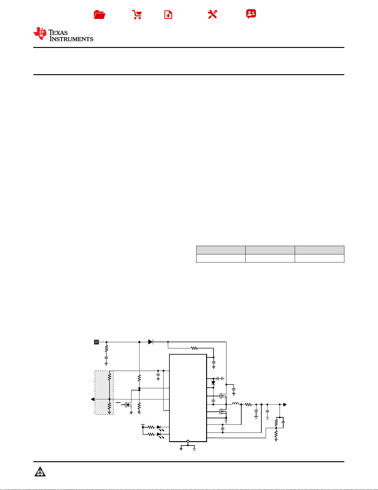
3 Description
The BQ24650 device is a highly integrated switchmode battery charge controller. It provides input
voltage regulation, which reduces charge current
when input voltage falls below a programmed level.
When the input is powered by a solar panel, the input
regulation loop lowers the charge current so that the
solar panel can provide maximum power output.
The BQ24650 offers a constant-frequency
synchronous PWM controller with high accuracy
current and voltage regulation, charge
preconditioning, charge termination, and charge
status monitoring.
Device Information
PART NUMBER PACKAGE BODY SIZE (NOM)
BQ24650 VQFN (16) 3.50 mm × 3.50 mm
(1) For all available packages, see the orderable addendum at
the end of the data sheet.
(1)
Typical Application
1
An IMPORTANT NOTICE at the end of this data sheet addresses availability, warranty, changes, use in safety-critical applications,
intellectual property matters and other important disclaimers. PRODUCTION DATA.

BQ24650
SLUSA75B –JULY 2010–REVISED JANUARY 2020
www.ti.com
Table of Contents
1 Features.................................................................. 1
2 Applications ........................................................... 1
3 Description ............................................................. 1
4 Revision History..................................................... 2
5 Description (continued)......................................... 3
6 Pin Configuration and Functions......................... 4
7 Specifications......................................................... 5
7.1 Absolute Maximum Ratings ...................................... 5
7.2 ESD Ratings.............................................................. 5
7.3 Recommended Operating Conditions....................... 5
7.4 Thermal Information.................................................. 6
7.5 Electrical Characteristics........................................... 6
7.6 Typical Characteristics............................................ 10
8 Detailed Description............................................ 12
8.1 Overview ................................................................. 12
8.2 Functional Block Diagram....................................... 12
8.3 Feature Description................................................. 12
8.4 Device Functional Modes........................................ 21
9 Application and Implementation ........................ 23
9.1 Application Information............................................ 23
9.2 Typical Application ................................................. 23
10 Power Supply Recommendations..................... 29
11 Layout................................................................... 29
11.1 Layout Guidelines ................................................. 29
11.2 Layout Example .................................................... 30
12 Device and Documentation Support ................. 31
12.1 Device Support...................................................... 31
12.2 Receiving Notification of Documentation Updates 31
12.3 Support Resources ............................................... 31
12.4 Trademarks........................................................... 31
12.5 Electrostatic Discharge Caution............................ 31
12.6 Glossary................................................................ 31
13 Mechanical, Packaging, and Orderable
Information........................................................... 31
4 Revision History
Changes from Revision A (April 2016) to Revision B Page
• Changed Title ........................................................................................................................................................................ 1
• Deleted Component Values from Typical Application on Page 1. ......................................................................................... 1
Changes from Original (July 2010) to Revision A Page
• Added ESD Ratings table, Feature Description section, Device Functional Modes, Application and Implementation
section, Power Supply Recommendations section, Layout section, Device and Documentation Support section, and
Mechanical, Packaging, and Orderable Information section.................................................................................................. 1
• Removed Ordering Information table .................................................................................................................................... 1
2
Submit Documentation Feedback Copyright © 2010–2020, Texas Instruments Incorporated
Product Folder Links: BQ24650

BQ24650
www.ti.com
SLUSA75B –JULY 2010–REVISED JANUARY 2020
5 Description (continued)
The BQ24650 charges the battery in three phases: pre-conditioning, constant current, and constant voltage.
Charge is terminated when the current reaches 1/10 of the fast charge rate. The pre-charge timer is fixed at 30
minutes. The BQ24650 automatically restarts the charge cycle if the battery voltage falls below an internal
threshold and enters a low quiescent current sleep mode when the input voltage falls below the battery voltage.
The BQ24650 supports a battery from 2.1 V to 26 V with VFB set to a 2.1-V feedback reference. The charge
current is programmed by selecting an appropriate sense resistor. The BQ24650 is available in a 16 -pin, 3.5 mm
× 3.5 mm2thin QFN package.
Product Folder Links: BQ24650
Submit Documentation FeedbackCopyright © 2010–2020, Texas Instruments Incorporated
3
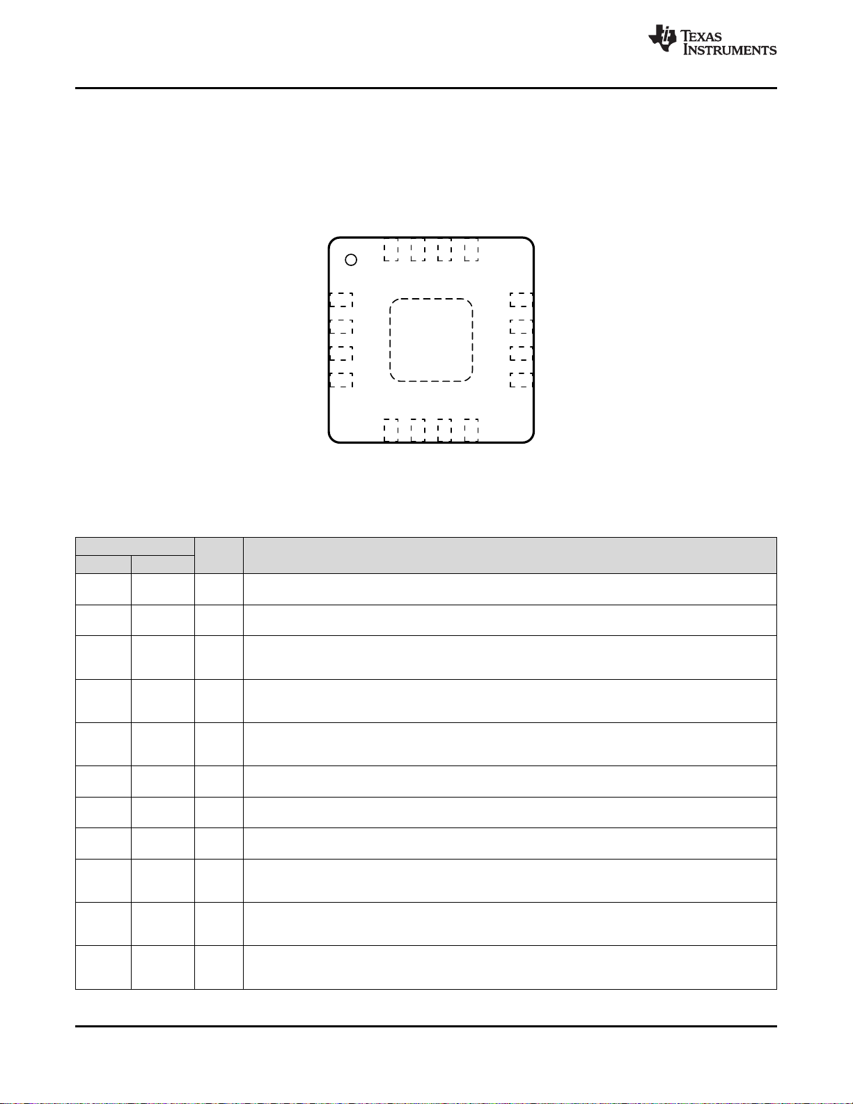
ThermalPad
16 BTST5STAT2
1VCC 12 REGN
15 HIDRV6VREF
2MPPSET 11 GND
14 PH7TERM_EN
3STAT1 10 SRP
13 LODRV8VFB
4TS 9 SRN
BQ24650
SLUSA75B –JULY 2010–REVISED JANUARY 2020
6 Pin Configuration and Functions
www.ti.com
RVA Package
16-Pin VQFN
Top View
PIN
NO. NAME
1 VCC P
2 MPPSET I
TYPE DESCRIPTION
IC power positive supply. Place a 1-μF ceramic capacitor from VCC to GND and place it as close as
possible to IC. Place a 10-Ω resistor from input side to VCC pin to filter the noise.
Input voltage set point. Use a voltage divider from input source to GND to set voltage on MPPSET to 1.2
V. To disable charge, pull MPPSET below 75 mV.
Open-drain charge status output to indicate various charger operation. Connect to the cathode of LED
3 STAT1 O
with 10 kΩ to the pullup rail. LOW or LED light up indicates charge in progress. Otherwise stays HI or
LED stays off. When any fault condition occurs, both STAT1 and STAT2 are HI, or both LEDs are off.
Temperature qualification voltage input. Connect to a negative temperature coefficient thermistor.
4 TS I
Program the hot and cold temperature window with a resistor divider from VREF to TS to GND. A 103AT2 thermister is recommended.
Open-drain charge status output to indicate various charger operation. Connect to the cathode of LED
5 STAT2 O
with 10 kΩ to the pullup rail. LOW or LED light up indicates charge is complete. Otherwise, stays HI or
LED stays off. When any fault condition occurs, both STAT1 and STAT2 are HI, or both LEDs are off.
6 VREF P
7 TERM_EN I
8 VFB I
3.3-V reference voltage output. Place a 1-μF ceramic capacitor from VREF to GND pin close to the IC.
This voltage could be used for programming voltage on TS and the pullup rail of STAT1 and STAT2.
Charge termination enable. Pull TERM_EN to GND to disable charge termination. Pull TERM_EN to
VREF to allow charge termination. TERM_EN must be terminated and cannot be left floating.
Charge voltage analog feedback adjustment. Connect the output of a resistor divider powered from the
battery terminals to this node to adjust the output battery voltage regulation.
Charge current sense resistor, negative input. A 0.1-μF ceramic capacitor is placed from SRN to SRP to
9 SRN I
10 SRP P/I
11 GND P
provide differential-mode filtering. An optional 0.1-μF ceramic capacitor is placed from SRN to GND for
common-mode filtering.
Charge current sense resistor, positive input. A 0.1-μF ceramic capacitor is placed from SRN to SRP to
provide differential-mode filtering. A 0.1-μF ceramic capacitor is placed from SRP to GND for commonmode filtering.
Power ground. Ground connection for high-current power converter node. On PCB layout, connect
directly to source of low-side power MOSFET, to ground connection of input and output capacitors of the
charger. Only connect to GND through the thermal pad underneath the IC.
Pin Functions
4
Submit Documentation Feedback Copyright © 2010–2020, Texas Instruments Incorporated
Product Folder Links: BQ24650
BQ24650
www.ti.com
SLUSA75B –JULY 2010–REVISED JANUARY 2020
Pin Functions (continued)
PIN
NO. NAME
12 REGN P
13 LODRV O
14 PH P
15 HIDRV O
16 BTST P PWM high-side driver positive supply. Connect the 0.1-µF bootstrap capacitor from PH to BTST.
—
Thermal
Pad
TYPE DESCRIPTION
PWM low-side driver positive 6-V supply output. Connect a 1-μF ceramic capacitor from REGN to GND,
close to the IC. Use to drive low-side driver and high-side driver bootstrap Schottky diode from REGN to
BTST.
PWM low-side driver output. Connect to the gate of the low-side N-channel power MOSFET with a short
trace.
Switching node, charge current output inductor connection. Connect the 0.1-μF bootstrap capacitor from
PH to BTST.
PWM high-side driver output. Connect to the gate of the high-side N-channel power MOSFET with a short
trace.
Exposed pad beneath the IC. The thermal pad must always be soldered to the board and have the vias
—
on the thermal pad plane star-connecting to GND and ground plane for high-current power converter. It
also serves as a thermal pad to dissipate heat.
7 Specifications
7.1 Absolute Maximum Ratings
over operating free-air temperature range (unless otherwise noted)
VCC, STAT1, STAT2, SRP, SRN –0.3 33
PH –2 36
Voltage (with respect to GND)
Maximum difference voltage SRP–SRN –0.5 0.5 V
Junction temperature, T
Storage temperature, T
(1) Stresses beyond those listed under Absolute Maximum Ratings may cause permanent damage to the device. These are stress ratings
only, and functional operation of the device at these or any other conditions beyond those indicated under Recommended Operating
Conditions is not implied. Exposure to absolute-maximum-rated conditions for extended periods may affect device reliability.
(2) All voltages are with respect to GND if not specified. Currents are positive into, negative out of the specified terminal. Consult Packaging
Section of the data book for thermal limitations and considerations of packages.
(3) Must have a series resistor between battery pack to VFB if battery pack voltage is expected to be greater than 16 V. Usually the resistor
divider top resistor takes care of this.
J
stg
VFB –0.3 16
REGN, LODRV, TS, MPPSET, TERM_EN –0.3 7
BTST, HIDRV with respect to GND –0.3 39
VREF –0.3 3.6
(1)(2)(3)
MIN MAX UNIT
V
–40 155 °C
–55 155 °C
7.2 ESD Ratings
V
(ESD)
(1) JEDEC document JEP155 states that 500-V HBM allows safe manufacturing with a standard ESD control process.
(2) JEDEC document JEP157 states that 250-V CDM allows safe manufacturing with a standard ESD control process.
Electrostatic discharge
Human-body model (HBM), per ANSI/ESDA/JEDEC JS-001
Charged-device model (CDM), per JEDEC specification JESD22-C101
(1)
(2)
7.3 Recommended Operating Conditions
MIN MAX UNIT
VCC, STAT1, STAT2, SRP, SRN –0.3 28
PH –2 30
Voltage range (with respect to
GND)
VFB –0.3 14
REGN, LODRV, TS, MPPSET, TERM_EN –0.3 6.5
BTST, HIDRV with respect to GND –0.3 34
VREF 3.3
Submit Documentation FeedbackCopyright © 2010–2020, Texas Instruments Incorporated
Product Folder Links: BQ24650
VALUE UNIT
±2000
±500
V
V
5
BQ24650
SLUSA75B –JULY 2010–REVISED JANUARY 2020
www.ti.com
Recommended Operating Conditions (continued)
MIN MAX UNIT
Maximum difference voltage SRP–SRN –0.2 0.2 V
Junction temperature, T
J
–40 125 °C
7.4 Thermal Information
BQ24650
THERMAL METRIC
R
θJA
R
θJC(top)
R
θJB
ψ
JT
ψ
JB
R
θJC(bot)
Junction-to-ambient thermal resistance
Junction-to-case (top) thermal resistance 81 °C/W
Junction-to-board thermal resistance 16 °C/W
Junction-to-top characterization parameter
Junction-to-board characterization parameter
Junction-to-case (bottom) thermal resistance 4 °C/W
(1) For more information about traditional and new thermal metrics, see the Semiconductor and IC Package Thermal Metrics application
report, SPRA953.
(2) The junction-to-ambient thermal resistance under natural convection is obtained in a simulation on a JEDEC-standard, high-K board, as
specified in JESD51-7, in an environment described in JESD51-2a
(3) The junction-to-top characterization parameter, ψJT, estimates the junction temperature of a device in a real system and is extracted
from the simulation data for obtaining R
(4) The junction-to-board characterization parameter, ψJB, estimates the junction temperature of a device in a real system and is extracted
from the simulation data for obtaining R
, using a procedure described in JESD51-2a (sections 6 and 7).
θJA
, using a procedure described in JESD51-2a (sections 6 and 7).
θJA
(1)
UNITRVA (VQFN)
16 PINS
(2)
(3)
(4)
43.8 °C/W
0.6 °C/W
15.77 °C/W
7.5 Electrical Characteristics
5 V ≤ V
OPERATING CONDITIONS
V
VCC_OP
QUIESCENT CURRENTS
I
BAT
I
AC
CHARGE VOLTAGE REGULATION
V
REG
I
VFB
CURRENT REGULATION – FAST CHARGE
V
IREG_CHG
CURRENT REGULATION – PRE-CHARGE
V
PRECHG
≤ 28 V, –40°C < TJ+ 125°C, typical values are at TA= 25°C, with respect to GND (unless otherwise noted)
VCC
PARAMETER TEST CONDITIONS MIN TYP MAX UNIT
VCC input voltage operating range 5 28 V
Total battery discharge current (sum of
currents into VCC, BTST, PH, SRP,
SRN, VFB), VFB ≤ 2.1V
Battery discharge current (sum of
currents into BTST, PH, SRP, SRN,
VFB), VFB ≤ 2.1V
Adapter supply current (sum of current
into VCC pin)
Feedback regulation voltage 2.1 V
Charge voltage regulation accuracy
Leakage current into VFB pin VFB = 2.1 V 100 nA
SRP-SRN current sense voltage range V
Charge current regulation accuracy V
Precharge current sense voltage
range
VCC < VBAT, VCC > V
VCC > VBAT, VCC > V
VCC > VBAT, VCC > V
CE = HIGH, Charge done
VCC > VBAT, VCC > V
VCC > VBAT, VCC > V
CE = HIGH, charge done
VCC > VBAT, VCC > V
CE = HIGH, Charging, Qg_total = 10 nC
(SLEEP) 15 µA
UVLO
, CE = LOW 5 µA
UVLO
VCCLOWV
UVLO
VCCLOWV
VCCLOWV
,
, CE = LOW 0.7 1 mA
,
2 3 mA
,
25 mA
[1]
TJ= 0°C to 85°C –0.5% 0.5%
TJ= –40°C to 125°C –0.7% 0.7%
= V
IREG_CHG
IREG_CHG
V
IREG_PRCHG
– V
SRP
SRN
= 40 mV –3% 3%
= V
– V
SRP
SRN
40 mV
4 mV
5 µA
6
Submit Documentation Feedback Copyright © 2010–2020, Texas Instruments Incorporated
Product Folder Links: BQ24650
www.ti.com
Electrical Characteristics (continued)
BQ24650
SLUSA75B –JULY 2010–REVISED JANUARY 2020
5 V ≤ V
≤ 28 V, –40°C < TJ+ 125°C, typical values are at TA= 25°C, with respect to GND (unless otherwise noted)
VCC
PARAMETER TEST CONDITIONS MIN TYP MAX UNIT
Precharge current regulation accuracy V
IREG_PRECH
CHARGE TERMINATION
V
TERMCHG
Termination current sense voltage
range
Termination current accuracy V
V
ITERM
ITERM
Deglitch time for termination (both
edges)
t
QUAL
I
QUAL
Termination qualification time V
Termination qualification current
BAT
Discharge current once termination is
detected
INPUT VOLTAGE REGULATION
V
MPPSET
MPPSET regulation voltage 1.2 V
Input voltage regulation accuracy –0.6% 0.6%
I
MPPSET
V
MPPSET_CD
V
MPPSET_CE
Leakage current into MPPSET pin V
MPPSET
MPPSET shorted to disable charge 75 mV
MPPSET released to enable charge 175 mV
INPUT UNDERVOLTAGE LOCKOUT COMPARATOR (UVLO)
V
UVLO
V
UVLO_HYS
AC undervoltage rising threshold Measure on VCC 3.65 3.85 4 V
AC undervoltage hysteresis, falling 350 mV
VCC LOWV COMPARATOR
V
VCC LOWV_fall
V
VCC LOWV_rise
Falling threshold, disable charge Measure on VCC 4.1 V
Rising threshold, resume charge 4.35 V
SLEEP COMPARATOR (REVERSE DISCHARGING PROTECTION)
V
SLEEP _FALL
V
SLEEP_HYS
SLEEP falling threshold V
VCC
SLEEP hysteresis 500 mV
SLEEP rising shutdown deglitch VCC falling below SRN 100 ms
SLEEP falling powerup deglitch
VCC rising above SRN, Delay to exit
SLEEP mode
BAT LOWV COMPARATOR
V
LOWV
V
LOWV_HYS
Precharge to fast charge transition
(LOWV threshold)
Measure on VFB pin 1.54 1.55 1.56 V
LOWV hysteresis 100 mV
LOWV rising deglitch VFB falling below V
LOWV falling deglitch VFB rising above V
RECHARGE COMPARATOR
V
RECHG
Recharge threshold (with respect to
V
)
REG
Measure on VFB pin 35 50 65 mV
Recharge rising deglitch VFB decreasing below V
Recharge falling deglitch VFB increasing above V
BAT OVERVOLTAGE COMPARATOR
V
OV_RISE
V
OV_FALL
Overvoltage rising threshold As percentage of V
Overvoltage falling threshold As percentage of V
INPUT OVERVOLTAGE COMPARATOR (ACOV)
V
ACOV
V
ACOV_HYS
AC overvoltage rising threshold on
VCC
AC overvoltage falling hysteresis 1 V
AC overvoltage deglitch (both edges) Delay to changing the STAT pins 1 ms
AC overvoltage rising deglitch Delay to disable charge 1 ms
= 4 mV –25% 25%
= V
SRP
– V
SRN
4 mV
= 4 mV –25% 25%
100 ms
> V
RECH
and I
CHG
< I
TERM
250 ms
2 mA
= 7 V, TA= 0 – 85°C 1 µA
– V
to enter SLEEP 40 100 150 mV
SRN
30 ms
LOWV
LOWV
FB
FB
+ V
RECHG
RECHG
LOWV_HYS
25 ms
25 ms
10 ms
10 ms
104%
102%
31 32 33 V
Product Folder Links: BQ24650
Submit Documentation FeedbackCopyright © 2010–2020, Texas Instruments Incorporated
7
BQ24650
SLUSA75B –JULY 2010–REVISED JANUARY 2020
Electrical Characteristics (continued)
www.ti.com
5 V ≤ V
≤ 28 V, –40°C < TJ+ 125°C, typical values are at TA= 25°C, with respect to GND (unless otherwise noted)
VCC
PARAMETER TEST CONDITIONS MIN TYP MAX UNIT
AC overvoltage falling deglitch Delay to resume charge 20 ms
THERMAL SHUTDOWN COMPARATOR
T
SHUT
T
SHUT_HYS
Thermal shutdown rising temperature Temperature increasing 145 °C
Thermal shutdown hysteresis 15 °C
Thermal shutdown rising deglitch Temperature increasing 100 µs
Thermal shutdown falling deglitch Temperature decreasing 10 ms
THERMISTOR COMPARATOR
V
LTF
V
LTF_HYS
V
HTF
V
TCO
Cold temperature rising threshold
Rising hysteresis 0.2% 0.4% 0.6%
Hot temperature rising threshold 46.7% 47.5% 48.3%
As percentage to V
Cut-off temperature rising threshold 44.3% 45% 45.7%
Deglitch time for temperature out of
range detection
Deglitch time for temperature in valid
range detection
VTS< V
VTS< V
VTS> V
VTS> V
CHARGE OVERCURRENT COMPARATOR (CYCLE-BY-CYCLE)
V
OC
Charge overcurrent rising threshold
Current rising, in synchronous mode
measure (V
CHARGE UNDERCURRENT COMPARATOR (CYCLE-BY-CYCLE)
V
ISYNSET
Charge undercurrent falling threshold Switch from CCM to DCM, V
BATTERY-SHORTED COMPARATOR (BATSHORT)
V
BATSHT
V
BATSHT_HYS
t
BATSHT_DEG
BAT short falling threshold, forced
non-synchronous mode
V
SRP
BAT short rising hysteresis 200 mV
Deglitch on both edges 1 µs
LOW CHARGE CURRENT COMPARATOR
V
LC
V
LC_HYS
t
LC_DEG
Low charge current falling threshold Measure V
Low charge current rising hysteresis 1.25 mV
Deglitch on both edges 1 µs
VREF REGULATOR
V
VREF_REG
I
VREF_LIM
VREF regulator voltage V
VREF current limit V
VCC
VREF
REGN REGULATOR
V
REGN_REG
I
REGN_LIM
REGN regulator voltage V
REGN current limit
VCC
V
REGN
75 mV
BATTERY DETECTION
t
WAKE
I
WAKE
t
DISCHARGE
I
DISCHARGE
I
FAULT
I
QUAL
t
QUAL
V
WAKE
V
DISCH
Wake timer Max time charge is enabled 500 ms
Wake current R
SENSE
Discharge timer Max time discharge current is applied 1 sec
Discharge current 6 mA
Fault current after a timeout fault 2 mA
Termination qualification current 2 mA
Termination qualification time 250 ms
Wake threshold (with respect to V
Discharge threshold
Voltage on VFB to detect battery absent
)
REG
during wake
Voltage on VFB to detect battery absent
during discharge
72.5% 73.5% 74.5%
VREF
, or VTS< V
LTF
HTF
– V
LTF
HTF
SRP
LTF_HYS
– V
TCO
or VTS>V
)
SRN
, or
TCO
, or
400 ms
20 ms
80 mV
> 2.2V 1 5 9 mV
SRP
falling 2 V
(SRP-SRN)
> V
, 0 – 35 mA load 3.267 3.3 3.333 V
UVLO
= 0 V, V
VCC
> V
UVLO
1.25 mV
35 mA
> 10 V, MPPSET > 175 mV 5.7 6.0 6.3 V
= 0 V, V
VCC
> V
, MPPSET <
UVLO
40 mA
= 10 mΩ 50 125 200 mA
50 mV
1.55 V
8
Submit Documentation Feedback Copyright © 2010–2020, Texas Instruments Incorporated
Product Folder Links: BQ24650
www.ti.com
Electrical Characteristics (continued)
BQ24650
SLUSA75B –JULY 2010–REVISED JANUARY 2020
5 V ≤ V
≤ 28 V, –40°C < TJ+ 125°C, typical values are at TA= 25°C, with respect to GND (unless otherwise noted)
VCC
PARAMETER TEST CONDITIONS MIN TYP MAX UNIT
PWM HIGH-SIDE DRIVER (HIDRV)
R
DS_HI_ON
R
DS_HI_OFF
V
BTST_REFRESH
High-side driver (HSD) turnon
resistance
VBTST – VPH = 5.5 V 3.3 6 Ω
High-side driver turnoff resistance 1 1.4 Ω
Bootstrap refresh comparator
threshold Voltage
VBTST – VPH when low side refresh pulse
is requested
PWM LOW-SIDE DRIVER (LODRV)
R
DS_LO_ON
R
DS_LO_OFF
Low-side driver (LSD) turn-on
resistance
Low-side driver turn-off resistance 1 1.4 Ω
PWM DRIVERS TIMING
Driver dead-time
Dead time when switching between LSD
and HSD, No load at LSD and HSD
PWM OSCILLATOR
V
RAMP_HEIGHT
PWM ramp height As percentage of VCC 7%
PWM switching frequency 510 600 690 kHz
INTERNAL SOFT START (8 STEPS TO REGULATION CURRENT ICHG)
Soft-start steps 8 step
Soft-start step time 1.6 ms
CHARGER SECTION POWER-UP SEQUENCING
Charge-enable delay after power-up
Delay from MPPSET > 175 mV to charger
is allowed to turn on
LOGIC IO PIN CHARACTERISTICS (STAT1, STAT2, TERM_EN)
V
OUT_LOW
I
OUT_HI
V
IN_LOW
V
IN_HI
I
IN_BIAS
STAT1, STAT2 output low saturation
voltage
Sink current = 5 mA 0.5 V
Leakage current V = 32 V 1.2 µA
TERM_EN input low threshold voltage 0.4 V
TERM_EN input high threshold
voltage
TERM_EN bias current V
TERM_EN
= 0.5 V 60 µA
4.0 4.2 V
4.1 7 Ω
30 ns
1.5 s
1.6 V
Product Folder Links: BQ24650
Submit Documentation FeedbackCopyright © 2010–2020, Texas Instruments Incorporated
9
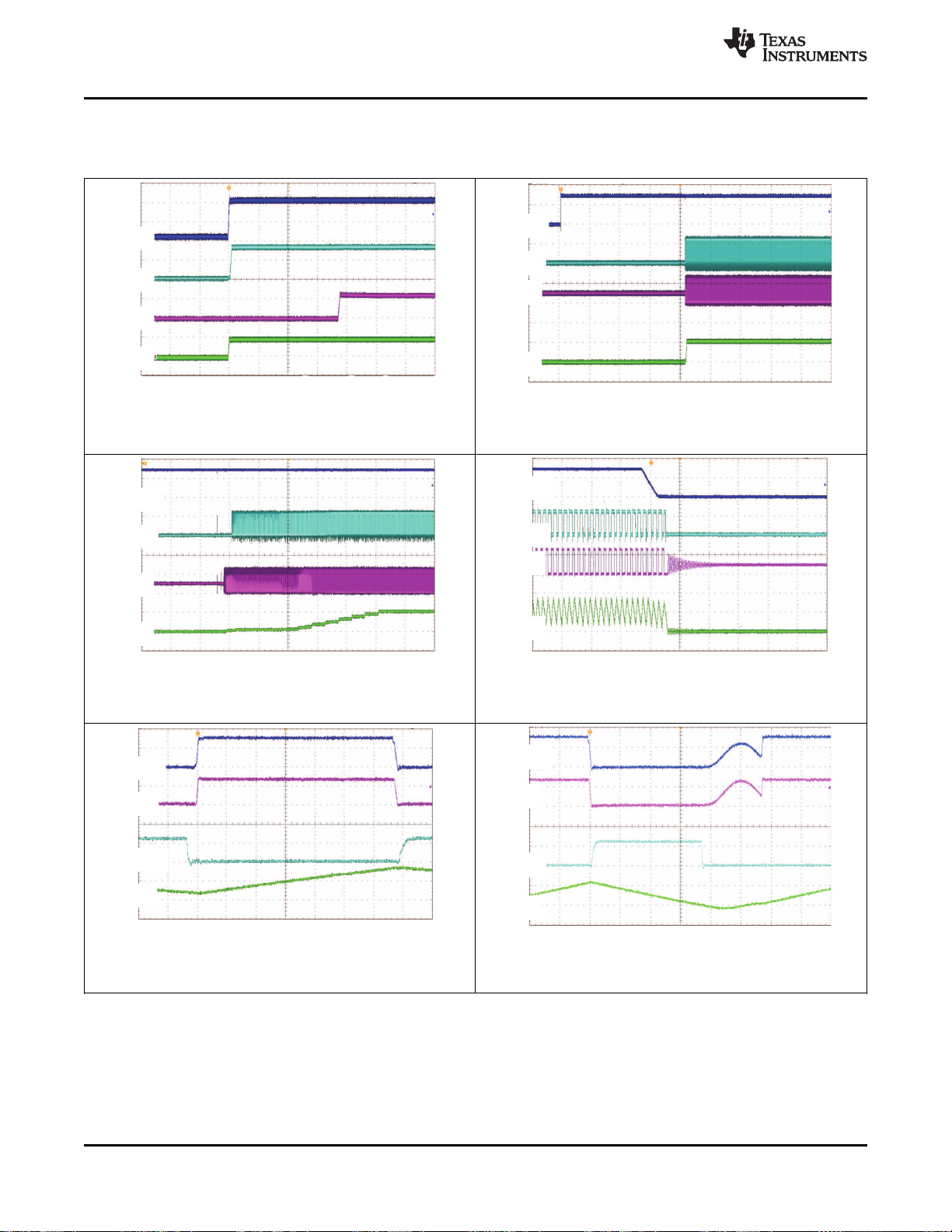
HIDRV
20V/div
LODRV
5V/div
PH
20V/div
IL
1A/div
200 ns/div
HIDRV
20V/div
LODRV
5V/div
PH
20V/div
IL
1A/div
100 ns/div
MPPSET
1V/div
LODRV
5V/div
PH
20V/div
IBAT
1A/div
10 s/divm
MPPSET
1V/div
LODRV
5V/div
PH
20V/div
IBAT
1A/div
4 ms/div
400 ms/div
MPPSET
1V/div
LODRV
5V/div
PH
20V/div
IBAT
1A/div
VCC
10V/div
VREF
2V/div
REGN
5V/div
STAT1
20V/div
800 s/divm
BQ24650
SLUSA75B –JULY 2010–REVISED JANUARY 2020
7.6 Typical Characteristics
VCC= 25 V, BQ24650 application circuit, TA= 25°C unless otherwise noted
www.ti.com
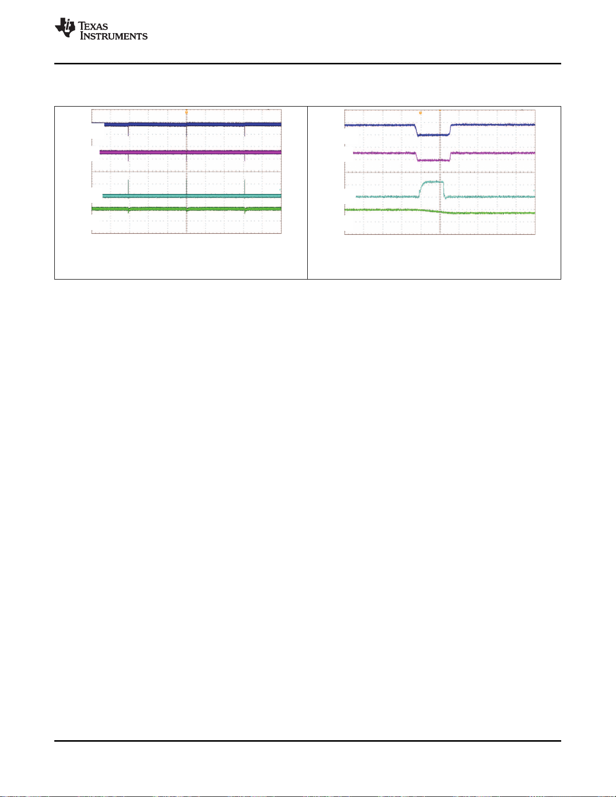
Figure 1. Power Up on V
CC
Figure 3. Charge Soft Start on MPPSET
Figure 2. Charge Start on MPPSET
Figure 4. Charge Stop on MPPSET
10
Figure 5. Switching in Continuous Conduction Mode
Figure 6. Switching in Discontinuous Conduction Mode
Submit Documentation Feedback Copyright © 2010–2020, Texas Instruments Incorporated
Product Folder Links: BQ24650
HIDRV
20V/div
LODRV
5V/div
PH
20V/div
IL
1A/div
400 s/divm
HIDRV
20V/div
LODRV
5V/div
PH
20V/div
IL
1A/div
100 ns/div
www.ti.com
Typical Characteristics (continued)
VCC= 25 V, BQ24650 application circuit, TA= 25°C unless otherwise noted
BQ24650
SLUSA75B –JULY 2010–REVISED JANUARY 2020
Figure 7. Switching at 100% Duty Cycle
Figure 8. Recharge the BTST-PH Capacitor
Product Folder Links: BQ24650
Submit Documentation FeedbackCopyright © 2010–2020, Texas Instruments Incorporated
11
VCC
BTST
HIDRV
PH
REGN
LODRV
GND
TS
VFB
SRP
6V LDO
V(SRP-SRN)
COMP
ERROR
AMPLIFIER
20 uA
1V
2.1 V
0.8V
SRN
STATE
MACHINE
LOGIC
BATTERY
DETECTION
LOGIC
VCC
PH
4V
+
_
BTST
REFRESH
CE
145 C°
IC Tj
TSHUT
SRN+100 mV
VCC
SLEEP
LEVEL
SHIFTER
+
-
+
-
+
-
+
-
+
-
V(SRP-SRN)
CHG_OCP
+
-
200% X IBAT_REG
SYNCH
SRP-SRN
IBAT_ REG
0.8V
0.8V
10
5
mV
20X
VFB
BAT_OVP
+
-
104% X 2.1V
LTF
+
-
HTF
VREF
TCO
+
-
+
-
SUSPEND
VCC
ACOV
+
-
32V
CE
VREF
STAT 1
STAT1
3.3V
LDO
VCC
VFB
LOWV
+
-
RCHRG
+
-
1.5V
+
-
2.05V
VFB
LOWV
RCHRG
TERM
+
-
V(SRP - SRN)
TERM
TERMINATE CHARGE
+
-
BQ24650
+
-
+
-
UVLO
V
UVLO
VCC
SLEEP
UVLO
PWM
CONTROL
LOGIC
+
-
PWM
+
-
+
-
+
-
STAT 2
+
-
CHARGE
20uA
DISCHARGE
CHARGE
8 mA
BAT_OVP
VOLTAGE
REFERENCE
VREF
0.8V
10
STAT2
30 Minute
Precharge
Timer
FAULT
FAULT
2 mA
DISCHARGE
MPPSET
1.2 V
+
-
175 mV
+
-
TERM_EN
FBO
EAI
EAO
Copyright © 2016, Texas Instruments Incorporated
BQ24650
SLUSA75B –JULY 2010–REVISED JANUARY 2020
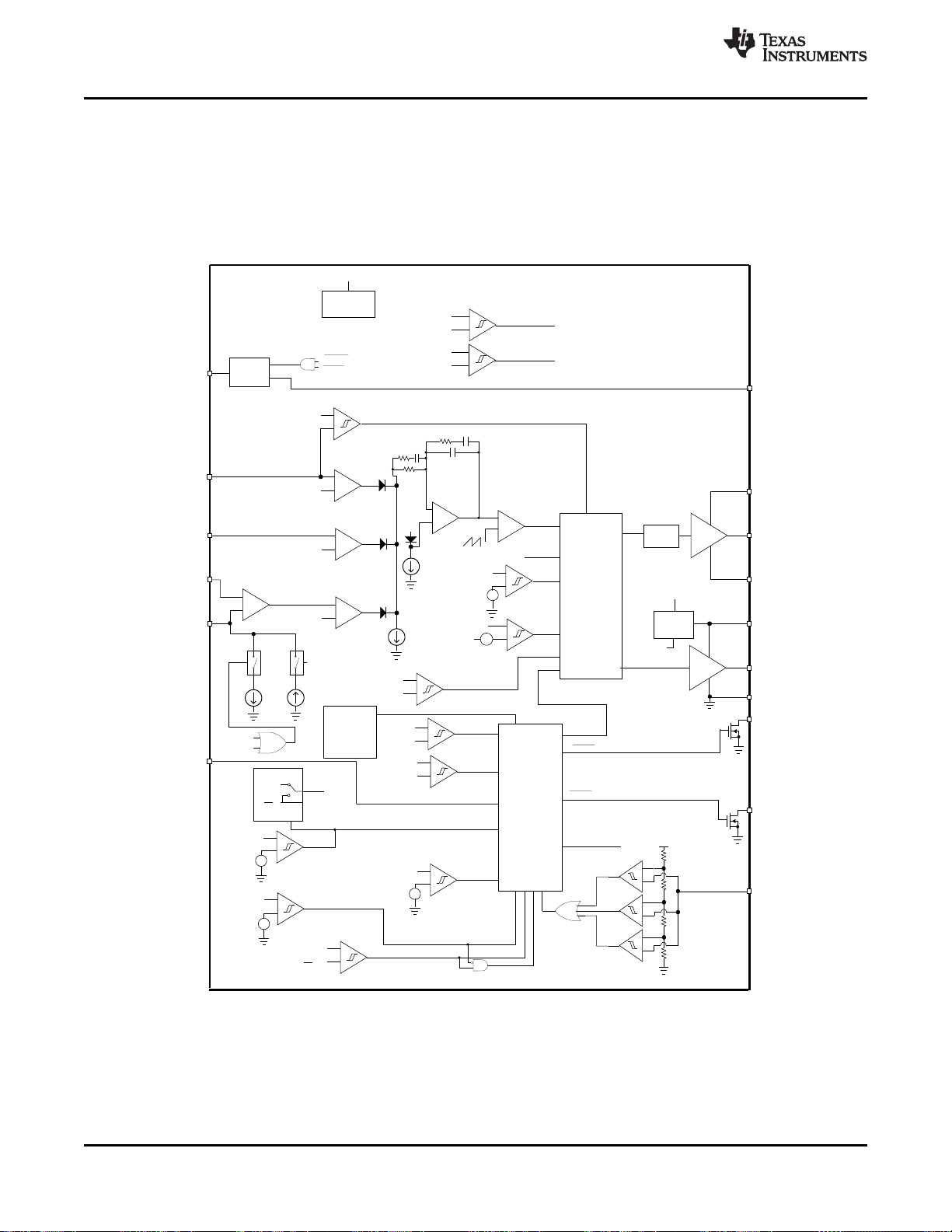
8 Detailed Description
8.1 Overview
The BQ24650 is a highly integrated solar input Li-ion or Li-polymer battery charge controller.
8.2 Functional Block Diagram
www.ti.com
8.3 Feature Description
8.3.1 Battery Voltage Regulation
The BQ24650 uses a high accuracy voltage regulator for the charging voltage. The charge voltage is
programmed through a resistor divider from the battery to ground, with the midpoint tied to the VFB pin. The
voltage at the VFB pin is regulated to 2.1 V, giving Equation 1 for the regulation voltage:
12
Submit Documentation Feedback Copyright © 2010–2020, Texas Instruments Incorporated
Product Folder Links: BQ24650
 Loading...