

Page 1
OAS
(bq24610)
OFB
(bq24617)
QFN-24
TOP VIEW
24 23 22 21 20 19
7 8 9 10 11 12
18
17
16
15
14
13
1
2
3
4
5
6
CE
ACN
ACP
ACDRV
STAT1
TS
SRN
SRP
ISET2
ACSET
GND
REGN
TTC
PG
STAT2
VREF
ISET1
VFB
VCC
BATDRV
BTST
HIDRV
PH
LODRV
bq24610
bq24617
www.ti.com
SLUS892 –DECEMBER 2009
Stand-Alone Synchronous Switch-Mode Li-Ion or Li-Polymer Battery Charger with System
1
FEATURES
Power Selector and Low I
Check for Samples: bq24610, bq24617
• 24-pin, 4×4-mm2QFN package
q
• 600 kHz NMOS-NMOS Synchronous Buck • Energy Star Low Quiescent Current I
Converter
• Stand-alone Charger Support for Li-Ion or
– < 15 µA Off-State Battery Discharge current
– < 1.5 mA Off-State Input Quiescent Current
Li-Polymer
• 5V–28V VCC Input Operating Range and APPLICATIONS Support 1-6 Battery Cells (bq24610)
• 5V–24V VCC Input Operating Range and
Support 1-5 Battery Cells (bq24617)
• Up to 10A Charge Current and Adapter Current
• High-Accuracy Voltage and Current Regulation
– ±0.5% Charge Voltage Accuracy
– ±3% Charge Current Accuracy
• Netbook, Mobile Internet Device and
Ultra-Mobile PC
• Personal Digital Assistants
• Handheld Terminals
• Industrial and Medical Equipment
• Portable Equipment
DESCRIPTION
– ±3% Adapter Current Accuracy
• Integration
– Automatic System Power Selection from
Adapter or Battery
– Internal Loop Compensation
– Internal Soft Start
– Dynamic Power Management
• Safety Protection
– Input Over-Voltage Protection
– Battery Thermistor Sense Hot/Cold Charge
Suspend
– Battery Detection
– Reverse Protection Input FET
– Programmable Safety Timer
– Charge Over-Current Protection
– Battery Short Protection
The bq24610/7 is highly integrated Li-ion or
Li-polymer switch-mode battery charge controller. It
offers a constant-frequency synchronous switching
PWM controller with high accuracy charge current
and voltage regulation, charge preconditioning,
termination, adapter current regulation and charge
status monitoring.
The bq24610/7 charges the battery in three phases:
preconditioning, constant current, and constant
voltage. Charge is terminated when the current
reaches a minimum user-selectable level. A
programmable charge timer provides a safety
backup. The bq24610/7 automatically restarts the
charge cycle if the battery voltage falls below an
internal threshold, and enters a low-quiescent current
sleep mode when the input voltage falls below the
battery voltage.
PACKAGE AND PIN-OUT
– Battery Over-Voltage Protection
– Thermal Shutdown
• Status Outputs
– Adapter Present
– Charger Operation Status
• Charge Enable Pin
• 6V Gate Drive for Synchronous Buck
Converter
• 30ns Driver Dead-time and 99.5% Max
Effective Duty Cycle
1
PRODUCTION DATA information is current as of publication date.
Products conform to specifications per the terms of the Texas
Instruments standard warranty. Production processing does not
necessarily include testing of all parameters.
Copyright © 2009, Texas Instruments Incorporated
Please be aware that an important notice concerning availability, standard warranty, and use in critical applications of Texas
Instruments semiconductor products and disclaimers thereto appears at the end of this data sheet.
q
Page 2
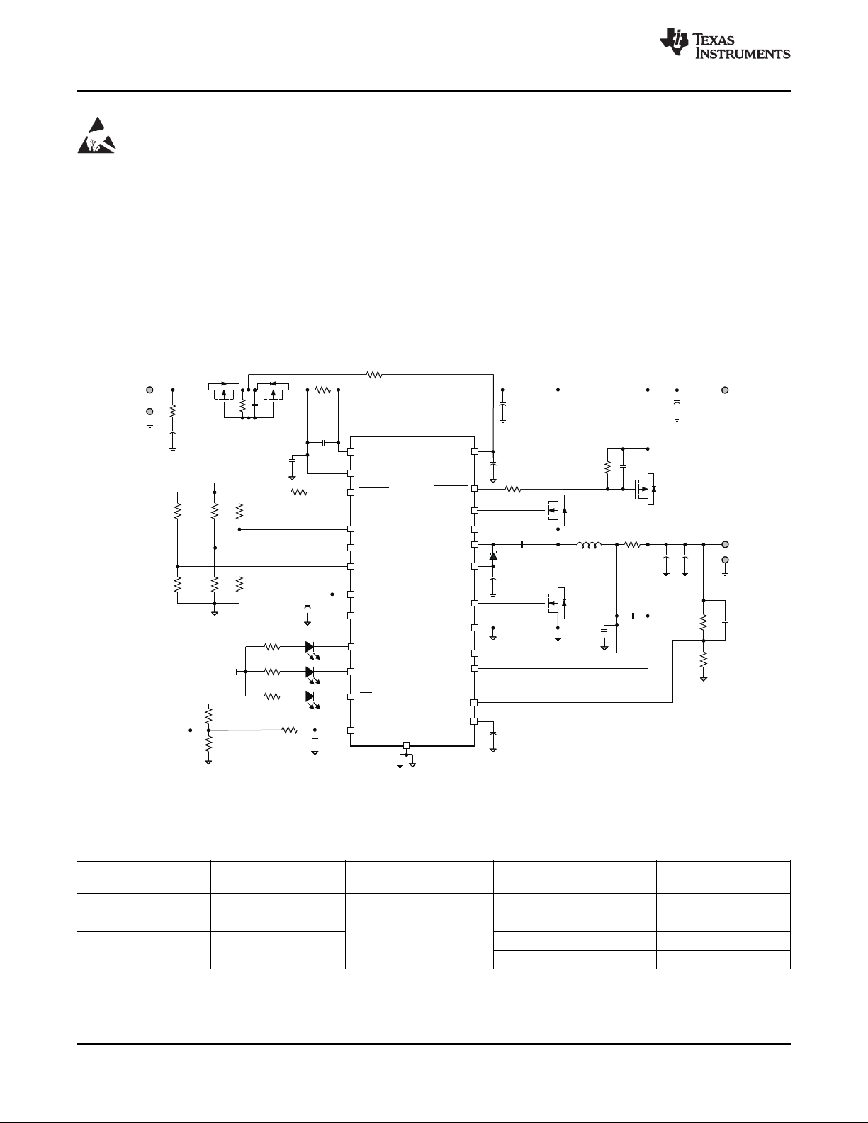
RAC
0.010 W
Q1 (ACFET)
N
P
ACN
ACP
ISET2
ACSET
VREF
CE
VFB
TS
VCC
HIDRV
N
PH
BTST
REGN
LODRV
GND
SRP
SRN
P
PACK+
PACK-
SYSTEM
ADAPTER+
ADAPTER-
C4
0.1 µF
C2
0.1 µF
C3 C7
Q4
Q5
C6
L1
6.8µH*
D1
BAT54
C5
C10
0.1
µF
TTC
CTTC
VREF
STAT2
Pack
Thermistor
Sense
BATDRV
ACDRV
bq24610
bq24617
P
Q2 (ACFET)
Q3 (BATFET)
VREF
ISET1
STAT1
VBAT
R9
9.31kW
R10
430kW
R1
100
kW
PG
ADAPTER +
Cff
22 pF
0.1 µF
1µF
C8
10 µF
1 µF
1 µF
RSR
0.010
W
C11
0.1
µF
C12
10 µF*
C13
10 µF*
R2
500 kΩ
R1210kW
R1110
kW
R1310kW
R3
100 kW
R4
32.4 kW
R5
100 kW
R6
10kW
R7
100 kW
R8
22.1 kW
R14
100 kW
C14
0.1 mF
R15
100
kW
C15
0.1
µF
PwrPad
0.056 Fμ
R16
100
W
C1
0.1 Fμ
103AT
SI7617DN
SI7616DN
SIS412DN
SIS412DN
SI7617DN
C9
10 μF
R17
10Ω
R20
2Ω
C16
2.2μF
R18
1kΩ
R19
1kΩ
D2
D3
D4
bq24610
bq24617
SLUS892 –DECEMBER 2009
This integrated circuit can be damaged by ESD. Texas Instruments recommends that all integrated circuits be handled with
appropriate precautions. Failure to observe proper handling and installation procedures can cause damage.
ESD damage can range from subtle performance degradation to complete device failure. Precision integrated circuits may be more
susceptible to damage because very small parametric changes could cause the device not to meet its published specifications.
DESCRIPTION (CONTINUED)
The bq24610/7 controls external switches to prevent battery discharge back to the input, connect the adapter to
the system, and to connect the battery to the system using 6-V gate drives for better system efficiency. The
bq24610/7 features Dynamic Power Management (DPM). These features reduce battery charge current when
the input power limit is reached to avoid overloading the AC adapter when supplying the load and the battery
charger simultaneously. A highly-accurate current-sense amplifier enables precise measurement of input current
from the AC adapter to monitor the overall system power.
TYPICAL APPLICATION
www.ti.com
VIN=19V, 3-cell, I
adapter_limit
PART NUMBER IC MARKING PACKAGE QUANTITY
bq24610 OAS
2 Submit Documentation Feedback Copyright © 2009, Texas Instruments Incorporated
bq24617 OFB
=4A, I
=3A, I
charge
Figure 1. Typical System Schematic
ORDERING INFORMATION
= I
pre-charge
=0.3A, 5 hour saftey timer
term
24-PIN 4×4 mm2QFN
Product Folder Link(s): bq24610 bq24617
ODERING NUMBER
(Tape andReel)
bq24610RGER 3000
bq24610RGET 250
bq24617RGER 3000
bq24617RGET 250
Page 3
bq24610
bq24617
www.ti.com
PACKAGE THERMAL DATA
PACKAGE θ
QFN – RGE
(1) This data is based on using the JEDEC High-K board and the exposed die pad is connected to a Cu pad on the board. This is
connected to the ground plane by a 2×2 via matrix. θJAhas 5% improvement by 3x3 via matrix.
(2) For the most current package and ordering information, see the Package Option Addendum at the end of this document, or see the TI
Web site at www.ti.com.
(1)(2)
JP
4°C/W 43°C/W 2.3 W 0.023 W/°C
θ
JA
TA= 25°C DERATING FACTOR
POWER RATING ABOVE TA= 25°C
ABSOLUTE MAXIMUM RATINGS
over operating free-air temperature range (unless otherwise noted)
VCC, ACP, ACN, SRP, SRN, BATDRV, ACDRV, CE, STAT1, STAT2, PG –0.3 to 33 V
PH –2 to 36 V
Voltage range
Maximum difference ACP–ACN, SRP–SRN –0.5 to 0.5 V
voltage
T
Junction temperature range –40 to 155 °C
J
T
Storage temperature range –55 to 155 °C
stg
(1) Stresses beyond those listed under absolute maximum ratings may cause permanent damage to the device. These are stress ratings
only, and functional operation of the device at these or any other conditions beyond those indicated under recommended operating
conditions is not implied. Exposure to absolute-maximum-rated conditions for extended periods may affect device reliability.
(2) All voltages are with respect to GND if not specified. Currents are positive into, negative out of the specified terminal. Consult Packaging
Section of the data book for thermal limitations and considerations of packages.
(3) Must have a series resistor between battery pack to VFB if Battery Pack voltage is expected to be greater than 16V. Usually the resistor
divider top resistor will take care of this.
VFB –0.3 to 16 V
REGN, LODRV, ACSET, TS, TTC –0.3 to 7 V
BTST, HIDRV with respect to GND –0.3 to 39 V
VREF, ISET1, ISET2 –0.3 to 3.6 V
(1) (2) (3)
SLUS892 –DECEMBER 2009
VALUE UNIT
RECOMMENDED OPERATING CONDITIONS
VALUE UNIT
VCC, ACP, ACN, SRP, SRN, BATDRV, ACDRV, CE, STAT1, STAT2, PG –0.3 to 28 V
PH –2 to 30 V
VFB –0.3 to 14 V
Voltage range REGN, LODRV, ACSET, TS, TTC –0.3 to 6.5 V
BTST, HIDRV with respect to GND –0.3 to 34 V
ISET1, ISET2 –0.3 to 3.3 V
VREF 3.3 V
Maximum difference ACP–ACN, SRP–SRN –0.2 to 0.2 V
voltage
T
Junction temperature range 0 to 125 °C
J
T
Storage temperature range –55 to 155 °C
stg
Copyright © 2009, Texas Instruments Incorporated Submit Documentation Feedback 3
Product Folder Link(s): bq24610 bq24617
Page 4
bq24610
bq24617
SLUS892 –DECEMBER 2009
ELECTRICAL CHARACTERISTICS
5.0V ≤ V(VCC) ≤ 28V, 0°C < TJ< +125°C, typical values are at TA= 25°C, with respect to GND (unless otherwise noted)
PARAMETER TEST CONDITIONS MIN TYP MAX UNIT
OPERATING CONDITIONS
V
VCC_OP
QUIESCENT CURRENTS
I
BAT
I
AC
CHARGE VOLTAGE REGULATION
V
FB
I
VFB
CURRENT REGULATION – FAST CHARGE
V
ISET1
V
IREG_CHG
K
ISET1
I
ISET1
CURRENT REGULATION – PRECHARGE
V
ISET2
K
ISET2
I
ISET2
VCC input voltage operating range(610) 5.0 28.0
VCC input voltage operating range(617) 5.0 24.0
Total battery discharge current (sum of
currents into VCC, BTST, PH, ACP, V
ACN, SRP, SRN, VFB), VFB ≤2.1 V
Battery discharge current (sum of
currents into BTST, PH, SRP, SRN,
VFB), VFB ≤ 2.1 V
Adapter supply current (current into V
VCC,ACP,ACN pin) done
< V
> V
> V
> V
> V
> V
SRN
SRN
SRN
SRN
SRN
SRN
, V
, V
, V
, V
, V
, V
VCC
V
VCC
V
VCC
done
V
VCC
current)
VCC
V
VCC
Qg_total = 20 nC
> V
VCC
UVLO
> V
VCC
UVLO
> V
VCC
VCCLOW
> V
VCC
UVLO
VCC>VVCCLOW
VCC>VVCCLOW
(SLEEP) 15 μA
CE = LOW 5 µA
CE = HIGH, Charge
CE = LOW (IC quiescent
, CE = HIGH, charge
, CE = HIGH, Charging,
1 1.5
2 5 mA
25
Feedback regulation voltage 2.1 V
Charge voltage regulation accuracy
TJ= 0°C to 85°C –0.5% 0.5%
TJ= -40°C to 125°C –0.7% 0.7%
Leakage current into VFB pin VFB = 2.1 V 100 nA
ISET1 voltage range 2 V
SRP-SRN current sense voltage range V
Charge current set factor (amps of
charge current per volt on ISET1 pin)
Charge current regulation accuracy
Leakage current into ISET1 pin V
R
V
V
V
V
= V
IREG_CHG
= 10 mΩ 5 A/V
SENSE
IREG_CHG
IREG_CHG
IREG_CHG
IREG_CHG
= 2 V 100 nA
ISET1
– V
SRP
SRN
= 40 mV –3% 3%
= 20 mV –4% 4%
= 5 mV –25% 25%
= 1.5 mV (V
> 3.1V) –40% 40%
SRN
ISET2 voltage range 2 V
Precharge current set factor (amps of
precharge current per volt on ISET2 pin)
Precharge current regulation accuracy V
Leakage current into ISET2 pin V
R
= 10 mΩ 1 A/V
SENSE
V
IREG_PRECH
IREG_PRECH
V
IREG_PRECH
ISET2
= 20 mV –4% 4%
= 5 mV –25% 25%
= 1.5 mV (V
< 3.1V) –55% 55%
SRN
= 2V 100 nA
www.ti.com
5 µA
100 mV
V
4 Submit Documentation Feedback Copyright © 2009, Texas Instruments Incorporated
Product Folder Link(s): bq24610 bq24617
Page 5
bq24610
bq24617
www.ti.com
ELECTRICAL CHARACTERISTICS (continued)
5.0V ≤ V(VCC) ≤ 28V, 0°C < TJ< +125°C, typical values are at TA= 25°C, with respect to GND (unless otherwise noted)
PARAMETER TEST CONDITIONS MIN TYP MAX UNIT
CHARGE TERMINATION
K
TERM
t
QUAL
I
QUAL
INPUT CURRENT REGULATION
V
ACSET
V
IREG_DPM
K
ACSET
I
ACSET
I
ISET1
INPUT UNDER-VOLTAGE LOCK-OUT COMPARATOR (UVLO)
V
UVLO
V
UVLO_HYS
VCC LOWV COMPARATOR
SLEEP COMPARATOR (REVERSE DISCHARGING PROTECTION)
V
SLEEP _FALL
V
SLEEP_HYS
ACN / SRN COMPARATOR
V
ACN-SRN_FALL
V
ACN-SRN_HYS
BAT LOWV COMPARATOR
V
LOWV
V
LOWV_HYS
RECHARGE COMPARATOR
V
RECHG
Termination current set factor (Amps of
termination current per volt on ISET2 R
pin)
Termination current accuracy V
= 10 mΩ 1 A/V
SENSE
V
= 20 mV –4% 4%
ITERM
= 5 mV –25% 25%
ITERM
V
= 1.5 mV –45% 45%
ITERM
Deglitch time for termination (both edge) 100 ms
Termination qualification time V
BAT>VRECH
and I
CHG<ITERM
Termination qualification current Discharge current once termination is detected 2 mA
ACSET Voltage Range 2 V
ACP-ACN Current Sense Voltage
Range
Input current set factor (amps of input
current per volt on ACSET pin)
Input current regulation accuracy
leakage current in to ACSET pin
Leakage current in to ACSET pin V
V
R
V
V
V
= V
IREG_DPM
= 10 mΩ 5 A/V
SENSE
IREG_DPM
IREG_DPM
IREG_DPM
= 2 V 100 nA
ACSET
– V
ACP
ACN
= 40 mV –3% 3%
= 20 mV –4% 4%
= 5 mV –25% 25%
AC Under-voltage rising threshold Measure on VCC 3.65 3.85 4 V
AC Under-voltage hysteresis, falling 350 mV
Falling threshold, disable charge Measure on VCC 4.1 V
Rising threshold, resume charge 4.35 4.5 V
SLEEP falling threshold V
VCC
– V
to enter SLEEP 40 100 150 mV
SRN
SLEEP hysteresis 500 mV
SLEEP rising delay VCC falling below SRN, Delay to turn off ACFET 1 μs
SLEEP falling delay VCC rising above SRN, Delay to turn on ACFET 30 μs
SLEEP rising shutdown deglitch VCC falling below SRN, Delay to enter SLEEP mode 100 ms
SLEEP falling powerup deglitch VCC rising above SRN, Delay to exit SLEEP mode 30 ms
ACN to SRN falling threshold V
ACN
– V
to turn on BATFET 100 200 310 mV
SRN
ACN to SRN rising hysteresis 100 mV
ACN to SRN rising deglitch V
ACN to SRN falling deglitch V
Precharge to fastcharge transition
(LOWV threshold)
– V
– V
SRN
SRN
> V
ACN-SRN_RISE
< V
ACN-SRN_FALL
ACN
ACN
Measured on VFB pin, Rising 1.534 1.55 1.566 V
LOWV hysteresis 100 mV
LOWV rising deglitch VFB falling below V
LOWV falling deglitch VFB rising above V
Recharge threshold (with-respect-to
V
)
REG
Measured on VFB pin, Falling 35 50 65 mV
Recharge rising deglitch VFB decreasing below V
Recharge falling deglitch VFB decreasing above V
LOWV
LOWV
+ V
RECHG
RECHG
LOWV_HYS
SLUS892 –DECEMBER 2009
250 ms
100 mV
2 ms
50 μs
25 ms
25 ms
10 ms
10 ms
Copyright © 2009, Texas Instruments Incorporated Submit Documentation Feedback 5
Product Folder Link(s): bq24610 bq24617
Page 6
bq24610
bq24617
SLUS892 –DECEMBER 2009
ELECTRICAL CHARACTERISTICS (continued)
5.0V ≤ V(VCC) ≤ 28V, 0°C < TJ< +125°C, typical values are at TA= 25°C, with respect to GND (unless otherwise noted)
PARAMETER TEST CONDITIONS MIN TYP MAX UNIT
BAT OVER-VOLTAGE COMPARATOR
V
OV_RISE
V
OV_FALL
INPUT OVER-VOLTAGE COMPARATOR (ACOV)
V
ACOV
V
ACOV_HYS
V
ACOV
V
ACOV_HYS
THERMAL SHUTDOWN COMPARATOR
T
SHUT
T
SHUT_HYS
THERMISTOR COMPARATOR
V
LTF
V
LTF_HYS
V
HTF
V
TCO
CHARGE OVER-CURRENT COMPARATOR (CYCLE-BY-CYCLE)
V
OC
CHARGE UNDER-CURRENT COMPARATOR (CYCLE-BY-CYCLE)
V
ISYNSET
BATTERY SHORTED COMPARATOR (BATSHORT)
V
BATSHT
V
BATSHT_HYS
V
BATSHT_DEG
LOW CHARGE CURRENT COMPARATOR
V
LC
V
LC_HYS
V
LC_DEG
VREF REGULATOR
V
VREF_REG
I
VREF_LIM
Over-voltage rising threshold As percentage of V
Over-voltage falling threshold As percentage of V
AC over-voltage rising threshold on
VCC (bq24610)
AC over-voltage falling hysteresis
(bq24610)
AC over-voltage rising threshold on
VCC (bq24617)
AC over-voltage falling
hysteresis(bq24617)
FB
FB
31.04 32 32.96 V
25.22 26 26.78 V
104%
102%
1 V
820 mV
AC over-voltage deglitch (both edge) Delay to changing the STAT pins 1 ms
AC over-voltage rising deglitch Delay to disable charge 1 ms
AC over-voltage falling deglitch Delay to resume charge 20 ms
Thermal shutdown rising temperature Temperature increasing 145 °C
Thermal shutdown hysteresis 15 °C
Thermal shutdown rising deglitch Temperature increasing 100 μs
Thermal shutdown falling deglitch Temperature decreasing 10 ms
Cold temperature rising threshold As Percentage to V
Rising hysteresis As Percentage to V
Hot temperature rising threshold As Percentage to V
Cut-off temperature rising threshold As Percentage to V
Deglitch time for temperature out of
range detection
Deglitch time for temperature in valid
range detection
VTS> V
VTS< V
LTF
LTF
, or VTS< V
– V
LTF_HYS
VREF
VREF
VREF
VREF
TCO
or VTS>V
, or VTS< V
TCO
HTF
, or VTS> V
HTF
Current rising, in non-synchronous mode, mesure on
Charge over-current falling threshold
V
Current rising, as percentage of V
synchronous mode, V
Charge over-current threshold floor 50 mV
Charge over-current threshold ceiling 180 mV
Minimum OCP threshold in synchronous mode,
measure on V
Maximum OCP threshold in synchronous mode,
measure on V
Charge under-current falling threshold Switch from SYNCH to NON-SYNCH, V
BAT Short falling threshold, forced
non-syn mode
V
, V
(SRP-SRN)
falling 2 V
SRP
< 2 V
SRP
(SRP-SRN)
(SRP-SRN)
SRP
, V
, V
> 2.2V
SRP
SRP
> 2.2V
> 2.2V
(IREG_CHG)
SRP
, in
> 2.2V 1 5 9 mV
72.5% 73.5% 74.5%
0.2% 0.4% 0.6%
36.2% 37% 37.8%
33.7% 34.4% 35.1%
400 ms
20 ms
45.5 mV
160%
BAT short rising hysteresis 200 mV
Deglitch on both edge 1 μs
Low charge current (average) falling
threshold to force into non-synchronous Measure on V
mode
(SRP-SRN)
1.25 mV
Low charge current rising hysteresis 1.25 mV
Deglitch on both edge 1 μs
VREF regulator voltage V
VREF current limit V
VCC
VREF
> V
, (0-35mA load) 3.267 3.3 3.333 V
UVLO
= 0V, V
VCC
> V
UVLO
35 mA
www.ti.com
6 Submit Documentation Feedback Copyright © 2009, Texas Instruments Incorporated
Product Folder Link(s): bq24610 bq24617
Page 7
bq24610
bq24617
www.ti.com
ELECTRICAL CHARACTERISTICS (continued)
5.0V ≤ V(VCC) ≤ 28V, 0°C < TJ< +125°C, typical values are at TA= 25°C, with respect to GND (unless otherwise noted)
PARAMETER TEST CONDITIONS MIN TYP MAX UNIT
REGN REGULATOR
V
REGN_REG
I
REGN_LIM
TTC INPUT AND SAFETY TIMER
T
PRECHG
T
CHARGE
K
TTC
BATTERY SWITCH (BATFET) DRIVER
R
DS_BAT_OFF
R
DS_BAT_ON
V
BATDRV_REG
AC SWITCH (ACFET) DRIVER
R
DS_AC_OFF
R
DS_AC_ON
V
ACDRV_REG
AC / BAT MOSFET DRIVERS TIMING
BATTERY DETECTION
t
WAKE
I
WAKE
t
DISCHARGE
I
DISCHARGE
I
FAULT
V
WAKE
V
DISCH
PWM HIGH SIDE DRIVER (HIDRV)
R
DS_HI_ON
R
DS_HI_OFF
V
BTST_REFRESH
PWM LOW SIDE DRIVER (LODRV)
R
DS_LO_ON
R
DS_LO_OFF
(1) Verified by design
REGN regulator voltage V
REGN current limit V
Precharge safety timer range
Fast charge saftey timer range, with +/-
10% accuracy
(1)
Fast charge timer accuracy
(1)
(1)
> 10V, CE = HIGH, (0-40mA load) 5.7 6.0 6.3 V
VCC
REGN
= 0V, V
VCC
> V
, CE = HIGH 40 mA
UVLO
Precharge time before fault occurs 1440 1800 2160 sec
Tchg = C
0.01 μF ≤ C
× K
TTC
TTC
≤ 0.11 μF –10% 10%
TTC
Timer multiplier 5.6 min/nF
V
below this threshold disables the safety timer and
TTC low threshold 0.4 V
TTC
termination
TTC oscillator high threshold 1.5 V
TTC oscillator low threshold 1 V
TTC source/sink current 45 50 55 μA
BATFET turn-off resistance V
BATFET turn-on resistance V
BATFET drive voltage 4.2 7 V
ACFET turn-off resistance V
ACFET turn-on resistance V
ACFET drive voltage 4.2 7 V
> 5V 150 Ω
ACN
> 5V 20 kΩ
ACN
V
BATDRV_REG
BATFET is on
VCC
VCC
V
ACDRV_REG
ACFET is on
= V
ACN
– V
BATDRV
when V
ACN
> 5V and
> 5V 30 Ω
> 5V 20 kΩ
= V
VCC
– V
ACDRV
when V
VCC
> 5V and
Driver dead time Dead time when switching between AC and BAT 10 μs
Wake time Max time charge is enabled 500 ms
Wake current R
= 10mΩ 50 125 200 mA
SENSE
Discharge time Max time discharge current is applied 1 sec
Discharge current 8 mA
Fault current after a timeout fault 2 mA
Wake threshold (with-respect-to V
Discharge threshold 1.55 V
High side driver (HSD) turn-on
resistance
High side driver turn-off resistance V
Bootstrap refresh comparator threshold
voltage
) Voltage on VFB to detect battery absent during Wake 50 mV
REG
Voltage on VFB to detect battery absent during
discharge
V
– VPH= 5.5 V 3.3 6 Ω
BTST
– VPH= 5.5 V 1 1.3 Ω
BTST
V
– VPHwhen low side refresh pulse is requested 4.0 4.2 V
BTST
Low side driver (LSD) turn-on resistance 4.1 7 Ω
Low side driver turn-off resistance 1 1.4 Ω
SLUS892 –DECEMBER 2009
1 10 Hr
Copyright © 2009, Texas Instruments Incorporated Submit Documentation Feedback 7
Product Folder Link(s): bq24610 bq24617
Page 8
bq24610
bq24617
SLUS892 –DECEMBER 2009
ELECTRICAL CHARACTERISTICS (continued)
5.0V ≤ V(VCC) ≤ 28V, 0°C < TJ< +125°C, typical values are at TA= 25°C, with respect to GND (unless otherwise noted)
PARAMETER TEST CONDITIONS MIN TYP MAX UNIT
PWM DRIVERS TIMING
Driver dead time 30 ns
PWM OSCILLATOR
V
RAMP_HEIGHT
INTERNAL SOFT START (8 steps to regulation current ICHG)
CHARGER SECTION POWER-UP SEQUENCING
LOGIC IO PIN CHARACTERISTICS (CE, STAT1, STAT2, PG)
V
IN_LO
V
IN_HI
V
BIAS_CE
V
OUT_LO
I
OUT_HI
PWM ramp height As percentage of VCC 7 %
PWM switching frequency
Soft start steps 8 step
Soft start step time 1.6 ms
Charge-enable delay after power-up Delay from CE=1 to charger is allowed to turn on 1.5 s
CE input low threshold voltage 0.8 V
CE input high threshold voltage 2.1
CE input bias current V = 3.3V (CE has internal 1MΩ pulldown resistor) 6 μA
STAT1, STAT2, PG output low
saturation voltage
Leakage current V = 32 V 1.2 µA
(2)
(2) Verified by design
Dead time when switching between LSD and HSD, no
load at LSD and HSD
510 600 690 kHz
Sink Current = 5 mA 0.5 V
www.ti.com
8 Submit Documentation Feedback Copyright © 2009, Texas Instruments Incorporated
Product Folder Link(s): bq24610 bq24617
Page 9
VCC
/PG
VREF
REGN
t − Time=4ms/div
5V/div
2V/div
10V/div
2V/div
t − Time=200ms/div
PH
LODRV
IBAT
CE
5V/div
5V/div
10V/div
2 A/div
t − Time=4ms/div
CE
PH
LODRV
IBAT
5V/div
5V/div
10V/div
2 A/div
t − Time=2 s/divμ
CE
PH
LODRV
IL
5V/div
5V/div
10V/div
2 A/div
www.ti.com
SLUS892 –DECEMBER 2009
TYPICAL CHARACTERISTICS
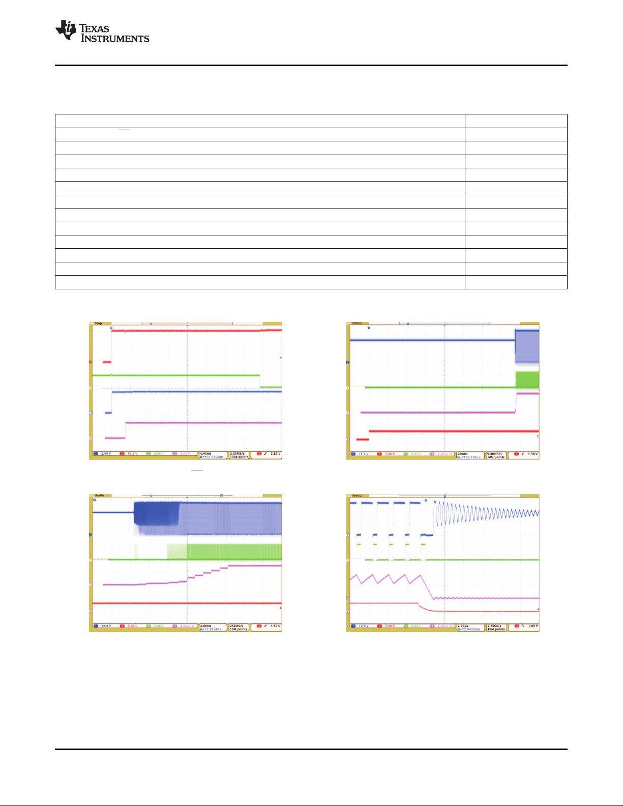
Table 1. Table of Graphs
Figure
REF REGN and PG Power Up (CE=1) Figure 2
Charge Enable Figure 3
Current Soft-Start (CE=1) Figure 4
Charge Disable Figure 5
Continuous Conduction Mode Switching Waveforms Figure 6
Cycle-by-Cycle Synchronous to Nonsynchronous Figure 7
100% Duty and Refresh Pulse Figure 8
Transient System Load (DPM) Figure 9
Battery Insertion Figure 10
Battery to Ground Short Protection Figure 11
Battery to ground Short Transition Figure 12
Efficiency vs Output Current Figure 13
bq24610
bq24617
Figure 2. REF REGN and PG Power Up (CE=1) Figure 3. Charge Enable
Figure 4. Current Soft-Start (CE=1) Figure 5. Charge Disable
Copyright © 2009, Texas Instruments Incorporated Submit Documentation Feedback 9
Product Folder Link(s): bq24610 bq24617
Page 10
t − Time=100ns/div
HIDRV
PH
LODRV
IL
2 A/div
20V/div
20V/div
5V/div
t − Time=100ns/div
PH
LODRV
IL
1 A/div
5V/div
5V/div
t − Time=400ns/div
PH
LODRV
IL
0.5 A/div
10V/div
5V/div
t − Time=200 s/divμ
IIN
ISYS
IBAT
2 A/div
2 A/div
2 A/div
t − Time=200ms/div
PH
IL
VBAT
2 A/div
5V/div
10V/div
t − Time=4ms/div
PH
IL
VBAT
LODRV
20V/div
5V/div
10V/div
2 A/div
bq24610
bq24617
SLUS892 –DECEMBER 2009
Figure 6. Continuous Conduction Mode Switching Waveform Figure 7. Cycle-by-Cycle Synchronous to Nonsynchronous
www.ti.com
Figure 8. 100% Duty and Refresh Pulse Figure 9. Transient System Load (DPM)
Figure 10. Battery Insertion Figure 11. Battery to GND Short Protection
10 Submit Documentation Feedback Copyright © 2009, Texas Instruments Incorporated
Product Folder Link(s): bq24610 bq24617
Page 11
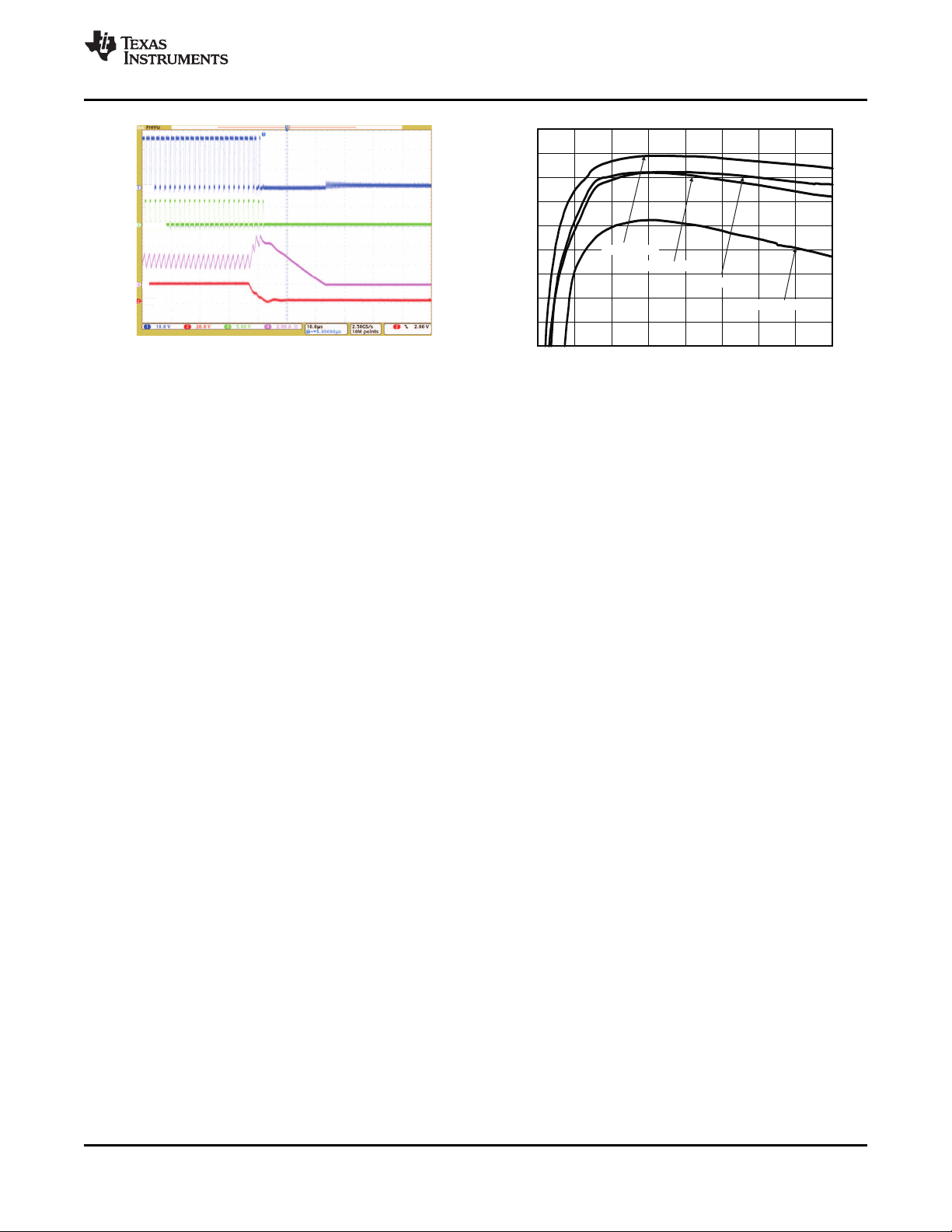
t − Time=10 s/divμ
PH
IL
VBAT
LODRV
20V/div
5V/div
10V/div
2 A/div
80
82
84
86
88
90
92
94
96
98
0 1 2 3
4
5
6
7
8
IBAT-OutputCurrent- A
Efficiency-%
12Vin,1cell
12Vin,2cell
20Vin,3cell
20Vin,4cell
www.ti.com
bq24610
bq24617
SLUS892 –DECEMBER 2009
Figure 12. Battery to GND Short Transition Figure 13. Efficiency vs Output Current
Copyright © 2009, Texas Instruments Incorporated Submit Documentation Feedback 11
Product Folder Link(s): bq24610 bq24617
Page 12

bq24610
bq24617
SLUS892 –DECEMBER 2009
Pin Functions – 24-Pin QFN
PIN
NO. NAME
1 ACN Adapter current sense resistor, negative input. A 0.1-μF ceramic capacitor is placed from ACN to ACP to provide differential-mode
filtering. An optional 0.1-μF ceramic capacitor is placed from ACN pin to GND for common-mode filtering.
2 ACP Adapter current sense resistor, positive input. A 0.1-μF ceramic capacitor is placed from ACN to ACP to provide differential-mode
filtering. A 0.1-μF ceramic capacitor is placed from ACP pin to GND for common-mode filtering.
3 ACDRV AC adapter to system MOSFET driver output. Connect through a 1-kΩ resistor to the gate of the ACFET P-channel power MOSFET
and the reverse conduction blocking P-channel power MOSFET. The internal gate drive is asymmetrical, allowing a quick turn-off and
slow turn-on, in addition to the internal break-before-make logic with respect to BATDRV. If needed, an optional capacitor from gate to
source of the ACFET is used to slow down the ON and OFF times.
4 CE Charge-enable active-HIGH logic input. HI enables charge. LO disables charge. It has an internal 1MΩ pull-down resistor.
5 STAT1 Open-drain charge status pin to indicate various charger operation (See Table 3)
6 TS Temperature qualification voltage input for battery pack negative temperature coefficient thermistor. Program the hot and cold
temperature window with a resistor divider from VREF to TS to GND. (See Figure 18)
7 TTC SafetyTimer and termination control. Connect a capacitor from this node to GND to set the timer. When this input is LOW, the timer
and termination are disabled. When this input is HIGH, the timer is disabled but termination is allowed.
8 PG Open-drain power-good status output. Active LOW when IC has a valid VCC (not in UVLO or ACOV or SLEEP mode). Active HIGH
when IC has an invalid VCC. PGcan be used to drive a LED or communicate with a host processor.
9 STAT2 Open-drain charge status pin to indicate various charger operation (See Table 3)
10 VREF 3.3V regulated voltage output. Place a 1-μF ceramic capacitor from VREF to GND pin close to the IC. This voltage could be used for
programming of voltage and current regulation and for programming the TS threshold.
11 ISET1 Fast Charge current set input. The voltage of ISET1 pin programs the fast charge current regulation set-point.
12 VFB Output voltage analog feedback adjustment. Connect the output of a resistive voltage divider from the battery terminals to this node to
adjust the output battery regulation voltage.
13 SRN Charge current sense resistor, negative input. A 0.1-μF ceramic capacitor is placed from SRN to SRP to provide differential-mode
filtering. An optional 0.1-μF ceramic capacitor is placed from SRN pin to GND for common-mode filtering.
14 SRP Charge current sense resistor, positive input. A 0.1-μF ceramic capacitor is placed from SRN to SRP to provide differential-mode
filtering. A 0.1-μF ceramic capacitor is placed from SRP pin to GND for common-mode filtering.
15 ISET2 Pre-charge and termination current set input. The voltage of ISET2 pin programs the pre-charge current regulation set-point and
termination current trigger point.
16 ACSET Adapter current set input. The voltage of ACSET pin programs the input current regulation set-point during Dynamic Power
Management (DPM)
17 GND Low-current sensitive analog/digital ground. On PCB layout, connect with PowerPad underneath the IC.
18 REGN PWM low side driver positive 6V supply output. Connect a 1-μF ceramic capacitor from REGN to GND pin, close to the IC. Use for
low side driver and high-side driver bootstrap voltage by connecting a small signal Schottky diode from REGN to BTST.
19 LODRV PWM low side driver output. Connect to the gate of the low-side power MOSFET with a short trace.
20 PH PWM high side driver negative supply. Connect to the Phase switching node (junction of the low-side power MOSFET drain, high-side
power MOSFET source, and output inductor). Connect the 0.1-μF bootstrap capacitor from PH to BTST.
21 HIDRV PWM high side driver output. Connect to the gate of the high-side power MOSFET with a short trace.
22 BTST PWM high side driver positive supply. Connect to the Phase switching node (junction of the low-side power MOSFET drain, high-side
power MOSFET source, and output inductor). Connect the 0.1-μF bootstrap capacitor from SW to BTST.
23 BATDRV Battery to system MOSFET driver output. Gate drive for the battery to system load BAT PMOS power FET to isolate the system from
the battery to prevent current flow from the system to the battery, while allowing a low impedance path from battery to system.
Connect this pin through a 1-kΩ resistor to the gate of the input BAT P-channel MOSFET. Connect the source of the FET to the
system load voltage node. Connect the drain of the FET to the battery pack positive terminal. The internal gate drive is asymmetrical
to allow a quick turn-off and slow turn-on, in addition to the internal break-before-make logic with respect to ACDRV. If needed, an
optional capacitor from gate to source of the BATFET is used to slow down the ON and OFF times.
24 VCC IC power positive supply. Connect through a 10-Ω to the common-source (diode-OR) point: source of high-side P-channel MOSFET
and source of reverse-blocking power P-channel MOSFET. Place a 1-μF ceramic capacitor from VCC to GND pin close to the IC.
PowerPAD Exposed pad beneath the IC. Always solder PowerPAD to the board, and have vias on the PowerPAD plane star-connecting to GND
and ground plane for high-current power converter. It also serves as a thermal pad to dissipate the heat.
FUNCTION DESCRIPTION
www.ti.com
12 Submit Documentation Feedback Copyright © 2009, Texas Instruments Incorporated
Product Folder Link(s): bq24610 bq24617
Page 13

VCC
ACDRV
BATDRV
BTST
HIDRV
PH
REGN
LODRV
GND
TS
bq24610/17
CE
ACP
ACN
VFB
SRP
6 VLDO
V(ACP-ACN)
+
-
V(SRP-SRN)
COMP
ERROR
AMPLIFIER
20µA
1V
2.1 V
IBAT_ REG
SRN
VCC
VCC-6 V
LDO
STATE
MACHINE
LOGIC
BATTERY
DETECTION
LOGIC
VCC
PH
4.2V
+
-
BTST REFRESH
SYSTEM
POWER
SELECTOR
LOGIC
CE
145 degC
ICTj
TSHUT
SRN+100 mV
VCC
SLEEP
LEVEL
SHIFTER
ACN
+
-
+
+
-
+
-
+
-
+
-
V(SRP-SRN)
CHG_OCP
+
-
160% XIBAT_REG
SYNCH
SRP-SRN
ISET1
ISET2
ACSET
IBAT_ REG
ISET1
ISET2
5 mV
20X
BAT
BAT_OVP
+
-
104% XVBAT_REG
LTF
+
-
HTF
VREF
TCO
+
-
+
-
SUSPEND
VCC
ACOV
+
-
V
ACOV
VREF
STAT 1
STAT1
20X
STAT 2
STAT2
3.3 V
LDO
VCC
VFB
LOWV
+
-
RCHRG
+
-
1.55V
+
-
2.05 V
VFB
RCHRG
TERM
+
-
V(SRP - SRN)
ISET2
TERM
TERMINATECHARGE
+
-
TTC
TTC
+
-
+
-
UVLO
V
UVLO
VCC
SLEEP
UVLO
VCC-6 V
VCC-6V
ACN-6V
ACN-6 V
LDO
ACN ACN-6 V
ACOV
PWM
CONTROL
LOGIC
+
-
PWM
+
-
+
-
+
-
PG
PG
+
-
CHARGE
20 µA
DISCHARGE
CHARGE
OR
DISCHARGE
8 mA
BAT_OVP
+
-
DISABLE
TMR/TERM
0.4 V
TTC
INTERNAL
REFERENCE
VREF
ACN-SRN
SRN+200 mV
+
-
ACN
Safety
Timer
TTC
FAULT
2 mA
FAULT
1M
CE
-
bq24610
bq24617
www.ti.com
BLOCK DIAGRAM
Figure 14. Functional Block Diagram for bq24610/7
Copyright © 2009, Texas Instruments Incorporated Submit Documentation Feedback 13
Product Folder Link(s): bq24610 bq24617
SLUS892 –DECEMBER 2009
Page 14

VCC > SRN
No
IndicateSLEEP
SLEEP MODE
Yes
EnableVREFLDO &
ChipBias
Turnon
BATDRVFET
30msdelay
TurnoffBATFET
Turnon ACFET
Battery
present?
Yes
Initiatebattery
detectalgorithm
Indicatebattery
absent
No
Conditionsmet
forcharge?
No
IndicateNOT
CHARGING,
Suspendtimers
Yes
VFB < VLOWV Yes
Start 30 minute
prechargetimer
IndicateCharge-
In-Progress
Regulate
prechargecurrent
VFB < VLOWV
Precharge
timerexpired?
Yes
No
Yes
IndicateFAULT
FAULT
EnableI
FAULT
VFB > VRECH
StartFastcharge
timer
IndicateCharge-
In-Progress
Regulate
fastchargecurrent
Fastcharge
TimerExpired?
No Yes
VFB > VRECH
&
ICHG < ITERM
Yes
No
IndicateChargeIn
Progress
Turnoffcharge,
EnableI
DISCHG
for 1
second
VFB < VRECH
No
IndicateDONE
ChargeComplete
Yes
IndicateBATTERY
ABSENT
BatteryRemoved
Yes
POR
See EnablingandDisabling
ChargeSection
Conditionsmet
forcharge?
No
Yes
No
Conditionsmet
forcharge?
No
Yes
IndicateNOT
CHARGING,
Suspendtimers
No
No
bq24610
bq24617
SLUS892 –DECEMBER 2009
OPERATIONAL FLOWCHART
www.ti.com
Figure 15. Operational Flowchart
14 Submit Documentation Feedback Copyright © 2009, Texas Instruments Incorporated
Product Folder Link(s): bq24610 bq24617
Page 15

V
LOWV
V
RECH
I
PRECH
& I
TERM
Precharge
Time
FastchargeSafetyTime
Precharge
Current
Regulation
Phase
FastchargeCurrent
RegulationPhase
FastchargeVoltage
RegulationPhase
Termination
Charge
Voltage
Charge
Current
RegulationCurrent
RegulationVoltage
R2
V = 2.1 V 1+ ,
BAT
R1
é ù
´
ê ú
ë û
ISET1
CHARGE
SR
V
I =
20 R´
www.ti.com
bq24610
bq24617
SLUS892 –DECEMBER 2009
DETAILED DESCRIPTION
Battery Voltage Regulation
The bq24610/7 uses a high accuracy voltage bandgap and regulator for the high charging voltage accuaracy.
The charge voltage is programmed via a resistor divider from the battery to ground, with the midpoint tied to the
VFB pin. The voltage at the VFB pin is regulated to 2.1V, giving the following equation for the regulation voltage:
where R2 is connected from VFB to the battery and R1 is connected from VFB to GND.
Battery Current Regulation
The ISET1 input sets the maximum fast charging current. Battery charge current is sensed by resistor R
connected between SRP and SRN. The full-scale differential voltage between SRP and SRN is 100mV. Thus, for
a 10mΩ sense resistor, the maximum charging current is 10A. The equation for charge current is:
V
voltage across RSRwith default value of 10mΩ. However, resistors of other values can also be used. A larger
sense resistor will give a larger sense voltage, a higher regulation accuracy; but, at the expense of higher
conduction loss.
Figure 16. Typical Charging Profile
, the input voltage range of ISET1 is between 0V and 2V. The SRP and SRN pins are used to sense
ISET1
(1)
SR
(2)
Copyright © 2009, Texas Instruments Incorporated Submit Documentation Feedback 15
Product Folder Link(s): bq24610 bq24617
Page 16

ACSET
DPM
AC
V
I =
20 R´
ISET2
PRECHARGE
SR
V
I =
100 R´
ISET2
TERM
SR
V
I =
100 R´
CHARGE TTC TTC
t = C K´
bq24610
bq24617
SLUS892 –DECEMBER 2009
Input Adapter Current Regulation
The total input from an AC adapter or other DC sources is a function of the system supply current and the battery
charging current. System current normally fluctuates as portions of the systems are powered up or down. Without
Dynamic Power Management (DPM), the source must be able to supply the maximum system current and the
maximum charger input current simultaneously. By using DPM, the battery charger reduces the charging current
when the input current exceeds the input current limit set by ACSET. The current capability of the AC adaptor
can be lowered, reducing system cost.
Similar to setting battery regulation current, adaptor current is sensed by resistor RACconnected between ACP
and ACN. Its maximum value is set by ACSET using Equation 3:
V
, the input voltage range of ACSET is between 0 and 2V. The ACP and ACN pins are used to sense
ACSET
voltage across RACwith default value of 10mΩ. However, resistors of other values can also be used. A larger the
sense resistor will give a larger sense voltage, and a higher regulation accuracy; but, at the expense of higher
conduction loss.
Precharge
On power-up, if the battery voltage is below the V
the battery. This feature is intended to revive deeply discharged cells. If the V
30 minutes of initiating precharge, the charger turns off and a FAULT is indicated on the status pins.
V
, the precharge current is determined by the voltage on the ISET2 pin according to Equation 4.
ISET2
threshold, the bq24610/7 applies the precharge current to
LOWV
threshold is not reached within
LOWV
www.ti.com
(3)
(4)
Charge Termination, Recharge, and Safety Timer
The bq24610/7 monitors the charging current during the voltage regulation phase. When V
termination is detected while the voltage on the VFB pin is higher than the V
current is less than the I
threshold, as calculated in Equation 5:
TERM
threshold AND the charge
RECH
The input voltage of ISET2 is between 0 and 2V. The minimum precharge/termination current is clamped to be
around 125mA with default 10mΩ sensing resistor. As a safety backup, the bq24610/7 also provides a
programmable charge timer. The charge time is programmed by the capacitor connected between the TTC pin
and GND, and is given by Equation 6
where C
GND, and K
(range from 0.01µF to 0.11 µF to give 1-10hr safety time) is the capacitor connected from TTC pin to
TTC
is the constant multiplier (5.6min/nF).
TTC
A new charge cycle is initiated and safety timer is reset when one of the following conditions occur:
• The battery voltage falls below the recharge threshold
• A power-on-reset (POR) event occurs
• CE is toggled
The TTC pin may be taken LOW to disable termination and to disable the safety timer. If TTC is pulled to VREF,
the bq24610/7 will continue to allow termination but disable the safety timer. TTC taken low will reset the safety
timer. When ACOV, VCCLOWV and SLEEP mode resume normal, the safety timer will be reset.
TTC
is valid,
(5)
(6)
16 Submit Documentation Feedback Copyright © 2009, Texas Instruments Incorporated
Product Folder Link(s): bq24610 bq24617
Page 17

bq24610
bq24617
www.ti.com
Power Up
The bq24610/7 uses a SLEEP comparator to determine the source of power on the VCC pin, since VCC can be
supplied either from the battery or the adapter. If the VCC voltage is greater than the SRN voltage, bq24610/7
will enable the ACFET and disable BATFET. If all other conditions are met for charging, bq24610/7 will then
attempt to charge the battery (See Enabling and Disabling Charging). If the SRN voltage is greater than VCC,
indicating that the battery is the power source, bq24610/7 enables the BATFET, and enters a low quiescent
current (<15μA) SLEEP mode to minimize current drain from the battery.
If VCC is below the UVLO threshold, the device is disabled, ACFET turns off and BATFET turns on.
Enable and Disable Charging
The following conditions have to be valid before charge is enabled:
• CE is HIGH
• The device is not in Under-Voltage-Lockout (UVLO) and not in VCCLOWV mode
• The device is not in SLEEP mode
• The VCC voltage is lower than the AC over-voltage threshold (VCC < V
• 30ms delay is complete after initial power-up
• The REGN LDO and VREF LDO voltages are at the correct levels
• Thermal Shut (TSHUT) is not valid
• TS fault is not detected
One of the following conditions will stop on-going charging:
• CE is LOW;
• Adapter is removed, causing the device to enter UVLO, VCCLOWV or SLEEP mode;
• Adapter is over voltage;
• The REGN or VREF LDOs are overloaded;
• TSHUT IC temperature threshold is reached (145°C on rising-edge with 15°C hysteresis).
• TS voltage goes out of range indicating the battery temperature is too hot or too cold.
• TTC safety timer out
ACOV
)
SLUS892 –DECEMBER 2009
System Power Selector
The bq24610/7 automatically switches adapter or battery power to the system load. The battery is connected to
the system by default during power up or during SLEEP mode. The battery is disconnected from the system and
then the adapter is connected to the system 30ms after exiting SLEEP. An automatic break-before-make logic
prevents shoot-through currents when the selectors switch.
The ACDRV is used to drive a pair of back-to-back p-channel power MOSFETs between adapter and ACP with
sources connected together and to VCC. The FET connected to adapter prevents reverse discharge from the
battery to the adapter when turned off. The p-channel FET with the drain connected to the adapter input provides
reverse battery discharge protection when off; and also minimizes system power dissipation, with its low-R
compared to a Schottky diode. The other p-channel FET connected to ACP separates battery from adapter, and
provides a limited dI/dt when connecting the adapter to the system by controlling the FET turn-on time. The
BATDRV controls a p-channel power MOSFET placed between BAT and system.
When adapter is not detected, the ACDRV is pulled to VCC to keep ACFET off, disconnecting the adapter from
system. BATDRV stays at ACN-6V to connect battery to system.
Approximately 30ms after the device comes out of SLEEP mode, the system begins to switch from battery to
adapter. The break-before-make logic keeps both ACFET and BATFET off for 10us before ACFET turns on. This
prevents shoot-through current or any large discharging current from going into the battery. The BATDRV is
pulled up to ACN and the ACDRV pin is set to VCC-6V by an internal regulator to turn on p-channel ACFET,
connecting the adapter to the system.
When the adapter is removed, the system waits until VCC drops back to within 200mV above SRN to switch from
adapter back to battery. The break-before-make logic still keeps 10μs dead time. The ACDRV is pulled up to
VCC and the BATDRV pin is set to ACN-6V by an internal regulator to turn on p-channel BATFET, connecting
the battery to the system.
DSON
,
Copyright © 2009, Texas Instruments Incorporated Submit Documentation Feedback 17
Product Folder Link(s): bq24610 bq24617
Page 18

o
o o
1
=
2 L C
f
p
bq24610
bq24617
SLUS892 –DECEMBER 2009
Asymmetrical gate drive (fast turn-off and slow turn-on) for the ACDRV and BATDRV drivers provides fast
turn-off and slow turn-on of the ACFET and BATFET to help the break-before-make logic and to allow a soft-start
at turn-on of either FET. The soft-start time can be further increased, by putting a capacitor from gate to source
of the p-channel power MOSFETs.
Automatic Internal Soft-Start Charger Current
The charger automatically soft-starts the charger regulation current every time the charger goes into fast-charge
to ensure there is no overshoot or stress on the output capacitors or the power converter. The soft-start consists
of stepping-up the charge regulation current into 8 evenly divided steps up to the programmed charge current.
Each step lasts around 1.6ms, for a typical rise time of 12.8ms. No external components are needed for this
function.
Converter Operation
The synchronous buck PWM converter uses a fixed frequency voltage mode with feed-forward control scheme. A
type III compensation network allows using ceramic capacitors at the output of the converter. The compensation
input stage is connected internally between the feedback output (FBO) and the error amplifier input (EAI). The
feedback compensation stage is connected between the error amplifier input (EAI) and error amplifier output
(EAO). The LC output filter is selected to give a resonant frequency of 12kHz–17kHz for bq24610/7, where
resonant frequency, fo, is given by:
www.ti.com
(7)
An internal saw-tooth ramp is compared to the internal EAO error control signal to vary the duty-cycle of the
converter. The ramp height is 7% of the input adapter voltage making it always directly proportional to the input
adapter voltage. This cancels out any loop gain variation due to a change in input voltage, and simplifies the loop
compensation. The ramp is offset by 300mV in order to allow zero percent duty-cycle when the EAO signal is
below the ramp. The EAO signal is also allowed to exceed the saw-tooth ramp signal in order to get a 100%
duty-cycle PWM request. Internal gate drive logic allows achieving 99.5% duty-cycle while ensuring the
N-channel upper device always has enough voltage to stay fully on. If the BTST pin to PH pin voltage falls below
4.2V for more than 3 cycles, then the high-side n-channel power MOSFET is turned off and the low-side
n-channel power MOSFET is turned on to pull the PH node down and recharge the BTST capacitor. Then the
high-side driver returns to 100% duty-cycle operation until the (BTST-PH) voltage is detected to fall low again
due to leakage current discharging the BTST capacitor below the 4.2 V, and the reset pulse is reissued.
The fixed frequency oscillator keeps tight control of the switching frequency under all conditions of input voltage,
battery voltage, charge current, and temperature, simplifying output filter design and keeping it out of the audible
noise region. Also see Application Information for how to select inductor, capacitor and MOSFET.
Synchronous and Non-Synchronous Operation
The charger operates in synchronous mode when the SRP-SRN voltage is above 5mV (0.5A inductor current for
a 10mΩ sense resistor). During synchronous mode, the internal gate drive logic ensures there is
break-before-make complimentary switching to prevent shoot-through currents. During the 30ns dead time where
both FETs are off, the body-diode of the low-side power MOSFET conducts the inductor current. Having the
low-side FET turn-on keeps the power dissipation low, and allows safely charging at high currents. During
synchronous mode the inductor current is always flowing and converter operates in continuous conduction mode
(CCM), creating a fixed two-pole system.
The charger operates in non-synchronous mode when the SRP-SRN voltage is below 5mV (0.5A inductor
current for a 10mΩ sense resistor). The charger is forced into non-synchronous mode when battery voltage is
lower than 2V or when the average SRP-SRN voltage is lower than 1.25mV.
During non-synchronous operation, the body-diode of lower-side MOSFET can conduct the positive inductor
current after the high-side n-channel power MOSFET turns off. When the load current decreases and the
inductor current drops to zero, the body diode will be naturally turned off and the inductor current will become
discontinuous. This mode is called Discontinuous Conduction Mode (DCM). During DCM, the low-side n-channel
power MOSFET will turn-on for around 80ns when the bootstrap capacitor voltage drops below 4.2V, then the
low-side power MOSFET will turn-off and stay off until the beginning of the next cycle, where the high-side power
MOSFET is turned on again. The 80ns low-side MOSFET on-time is required to ensure the bootstrap capacitor is
18 Submit Documentation Feedback Copyright © 2009, Texas Instruments Incorporated
Product Folder Link(s): bq24610 bq24617
Page 19

bq24610
bq24617
www.ti.com
always recharged and able to keep the high-side power MOSFET on during the next cycle. This is important for
battery chargers, where unlike regular dc-dc converters, there is a battery load that maintains a voltage and can
both source and sink current. The 80ns low-side pulse pulls the PH node (connection between high and low-side
MOSFET) down, allowing the bootstrap capacitor to recharge up to the REGN LDO value. After the 80ns, the
low-side MOSFET is kept off to prevent negative inductor current from occurring.
At very low currents during non-synchronous operation, there may be a small amount of negative inductor
current during the 80ns recharge pulse. The charge should be low enough to be absorbed by the input
capacitance. Whenever the converter goes into zero percent duty-cycle, the high-side MOSFET does not turn on,
and the low-side MOSFET does not turn on (only 80ns recharge pulse) either, and there is almost no discharge
from the battery.
During the DCM mode the loop response automatically changes and has a single pole system at which the pole
is proportional to the load current, because the converter does not sink current, and only the load provides a
current sink. This means at very low currents the loop response is slower, as there is less sinking current
available to discharge the output voltage.
Cycle-by-Cycle Charge Under Current Protection
If the SRP-SRN voltage decreases below 5mV (The charger is also forced into non-synchronous mode when the
average SRP-SRN voltage is lower than 1.25mV), the low side FET will be turned off for the remainder of the
switching cycle to prevent negative inductor current. During DCM, the low-side FET will only turn on for at around
80ns when the bootstrap capacitor voltage drops below 4.2V to provide refresh charge for the bootstrap
capacitor. This is important to prevent negative inductor current from causing a boost effect in which the input
voltage increases as power is transferred from the battery to the input capacitors and lead to an over-voltage
stress on the VCC node and potentially cause damage to the system.
SLUS892 –DECEMBER 2009
Input Over Voltage Protection (ACOV)
ACOV provides protection to prevent system damage due to high input voltage. Once the adapter voltage
reaches the ACOV threshold, charge is disabled and the system is switched to battery instead of adapter.
Input Under Voltage Lock Out (UVLO)
The system must have a minimum VCC voltage to allow proper operation. This VCC voltage could come from
either input adapter or battery, since a conduction path exists from the battery to VCC through the high side
NMOS body diode. When VCC is below the UVLO threshold, all circuits on the IC are disabled, and the gate
drive bias to ACFET and BATFET are disabled.
Battery Over-Voltage Protection
The converter will not allow the high-side FET to turn-on until the BAT voltage goes below 102% of the regulation
voltage. This allows one-cycle response to an over-voltage condition – such as occurs when the load is removed
or the battery is disconnected. An 8mA current sink from SRP to GND is on only during charge and allows
discharging the stored output inductor energy that is transferred to the output capacitors. BATOVP will also
suspend the safety timer.
Cycle-by-Cycle Charge Over-Current Protection
The charger has a secondary cycle-to-cycle over-current protection. It monitors the charge current, and prevents
the current from exceeding 160% of the programmed charge current. The high-side gate drive turns off when the
over-current is detected, and automatically resumes when the current falls below the over-current threshold.
Thermal Shutdown Protection
The QFN package has low thermal impedance, which provides good thermal conduction from the silicon to the
ambient, to keep junctions temperatures low. As added level of protection, the charger converter turns off and
self-protects whenever the junction temperature exceeds the TSHUT threshold of 145°C. The charger stays off
until the junction temperature falls below 130°C, then the charger will soft-start again if all other enable charge
conditions are valid. Thermal shutdown will also suspend the safety timer.
Copyright © 2009, Texas Instruments Incorporated Submit Documentation Feedback 19
Product Folder Link(s): bq24610 bq24617
Page 20

CHARGESUSPENDED CHARGESUSPENDED
TEMPERATURERANGE
TOINITIATECHARGE
TEMPERATURERANGE
DURING A CHARGE
CYCLE
V
LTF
GND
V
TCO
GND
V
LTFH
VREF
VREF
CHARGESUSPENDED CHARGESUSPENDED
V
HTF
V
LTF
V
LTFH
VR EF COLD HO T
LTF HT F
VR EF VRE F
HOT COLD
HTF LTF
1 1
V RTH RTH
V V
RT2 =
V V
RTH 1 RT H 1
V V
æ ö
´ ´ ´ -
ç ÷
è ø
æ ö æ ö
´ - - ´ -
ç ÷ ç ÷
è ø è ø
VREF
LTF
COLD
V
1
V
RT1 =
1 1
+
RT2 RTH
-
VREF
TS
RT2
RT1
RTH
103AT
bq24610/7
bq24610
bq24617
SLUS892 –DECEMBER 2009
Temperature Qualification
The controller continuously monitors battery temperature by measuring the voltage between the TS pin and
GND. A negative temperature coefficient thermistor (NTC) and an external voltage divider typically develop this
voltage. The controller compares this voltage against its internal thresholds to determine if charging is allowed.
To initiate a charge cycle, the battery temperature must be within the V(LTF) to V(HTF) thresholds. If battery
temperature is outside of this range, the controller suspends charge and the safety timer and waits until the
battery temperature is within the V(LTF) to V(HTF) range. During the charge cycle the battery temperature must
be within the V(LTF) to V(TCO) thresholds. If battery temperature is outside of this range, the controller suspends
charge and waits until the battery temperature is within the V(LTF) to V(HTF) range. The controller suspends
charge by turning off the PWM charge FETs. Figure below summarizes the operation.
www.ti.com
Figure 17. TS pin, Thermistor Sense Thresholds
Assuming a 103AT NTC thermistor on the battery pack as shown in Figure 1, the value RT1 and RT2 can be
determined by using the following equations:
(8)
(9)
20 Submit Documentation Feedback Copyright © 2009, Texas Instruments Incorporated
Figure 18. TS Resistor Network
Product Folder Link(s): bq24610 bq24617
Page 21

www.ti.com
bq24610
bq24617
SLUS892 –DECEMBER 2009
For example, 103AT NTC thermistors are used to monitor the battery pack temperature. Select T
T
= 40ºC then we get RT2= 430kΩ, RT1= 9.31kΩ and T
HOT
CUT-OFF
is around 45ºC. A small RC filter is suggested
COLD
= 0ºC and
to use for system-level ESD protection.
Timer Fault Recovery
The bq24610/7 provides a recovery method to deal with timer fault conditions. The following summarizes this
method:
Condition 1: The battery voltage is above the recharge threshold and a timeout fault occurs.
Recovery Method: The timer fault will clear when the battery voltage falls below the recharge threshold, and
battery detection will begin. Taking CE low or a POR condition will also clear the fault.
Condition 2: The battery voltage is below the recharge threshold and a timeout fault occurs.
Recovery Method: Under this scenario, the bq24610/7 applies the I
current to the battery. This small
FAULT
current is used to detect a battery removal condition and remains on as long as the battery voltage stays below
the recharge threshold. If the battery voltage goes above the recharge threshold, the bq24610/7 disables the
fault current and executes the recovery method described in Condition 1. Taking CE low or a POR condition will
also clear the fault.
PG Output
The open drain PG(power good) output indicates whether the VCC voltage is valid or not. The open drain FET
turns on whenever bq24610/7 has a valid VCC input ( not in UVLO or ACOV or SLEEP mode). The PGpin can
be used to drive an LED or communicate to the host processor.
CE (Charge Enable)
The CE digital input is used to disable or enable the charge process. A high-level signal on this pin enables
charge, provided all the other conditions for charge are met (see Enabling and Disabling Charge). A high to low
transition on this pin also resets all timers and fault conditions. There is an internal 1MΩ pulldown resistor on the
CE pin, so if CE is floated the charge will not turn on.
Inductor, Capacitor, and Sense Resistor Selection Guidelines
The bq24610/7 provides internal loop compensation. With this scheme, best stability occurs when the LC
resonant frequency, fo, is approximately 12kHz–17kHz for bq24610/7.
The following table provides a summary of typical LC components for various charge currents:
Table 2. Typical Inductor, Capacitor, and Sense Resistor Values as a Function of Charge Current for
bq24610/7 (600 kHz Switching Frequency)
CHARGE CURRENT 2A 4A 6A 8A 10A
Output Inductor Lo 6.8 μH 6.8 μH 4.7 μH 3.3 μH 3.3 μH
Output Capacitor Co 20 μF 20 μF 30 μF 40 μF 40 μF
Sense Resistor 10 mΩ 10 mΩ 10 mΩ 10 mΩ 10 mΩ
Charge Status Outputs
The open-drain STAT1 and STAT2 outputs indicate various charger operations as shown in the table below.
These status pins can be used to drive LEDs or communicate with the host processor. Note that OFF indicates
that the open-drain transistor is turned off.
Table 3. STAT Pin Definition for bq24610/7
CHARGE STATE STAT1 STAT2
Charge in progress ON OFF
Charge complete OFF ON
Charge suspend, timer fault, over-voltage, sleep mode, battery absent OFF OFF
Copyright © 2009, Texas Instruments Incorporated Submit Documentation Feedback 21
Product Folder Link(s): bq24610 bq24617
Page 22

PORorRECHARGE
Enable 125mA Charge,
Start 0.5stimer
VFB > V
RECH
No
BatteryPresent,
BeginCharge
0.5stimer
expired
Yes
No
Yes
Disable 125mA
Charge
Apply 8mA discharge
current, start 1stimer
VFB < V
LOWV
No
BatteryPresent,
BeginCharge
1stimer
expired
Yes
No
Yes
Disable 8mA
dischargecurrent
Thebatterydetectionroutinerunson
powerup, orifVFBfallsbelowVRECH
duetoremovingabatteryor
dischargingabattery
Battery Absent
bq24610
bq24617
SLUS892 –DECEMBER 2009
Battery Detection
For applications with removable battery packs, bq24610/7 provides a battery absent detection scheme to reliably
detect insertion or removal of battery packs.
www.ti.com
Figure 19. Battery Detection Flowchart
Once the device has powered up, an 8mA discharge current will be applied to the SRN terminal. If the battery
voltage falls below the LOWV threshold within 1 second, the discharge source is turned off, and the charger is
turned on at low charge current (125mA). If the battery voltage gets up above the recharge threshold within
500ms, there is no battery present and the cycle restarts. If either the 500ms or 1 second timer time out before
the respective thresholds are hit, a battery is detected and a charge cycle is initiated.
22 Submit Documentation Feedback Copyright © 2009, Texas Instruments Incorporated
Product Folder Link(s): bq24610 bq24617
Page 23

V
RECH
V
LOWV
Battery
inserted
Batterynotdetected
t
WAKE
Batterydetected
t
LOWV_DEG
t
RECH_DEG
V
REG
( )V
WAKE
( )V
DISH
DISC H DISCH
MAX
2
1
I t
C =
R
0.5 1+
R
´
é ù
´
ê ú
ë û
MAX
8mA 1sec
C = = 2.7 mF
500k
0.5 1+
100k
´
é ù
´
ê ú
ë û
www.ti.com
bq24610
bq24617
SLUS892 –DECEMBER 2009
Figure 20. Battery Detect Timing Diagram
Care must be taken that the total output capacitance at the battery node is not so large that the discharge current
source cannot pull the voltage below the LOWV threshold during the 1 second discharge time. The maximum
output capacitance can be calculated as follows:
(10)
Where C
is the maximum output capacitance, I
MAX
is the discharge current, t
DISCH
is the discharge time, and
DISCH
R2and R1are the voltage feedback resistors from the battery to the VFB pin. The 0.5 factor is the difference
between the RECHARGE and the LOWV thresholds at the VFB pin.
Example
For a 3-cell Li+ charger, with R2 = 500k, R1 = 100k (giving 12.6V for voltage regulation), I
DISCH
= 8mA, t
DISCH
= 1
second,
(11)
Based on these calculations, no more than 2.7 mF should be allowed on the battery node for proper operation of
the battery detection circuit.
Component List for Typical System Circuit of Figure 1
PART DESIGNATOR QTY DESCRIPTION
Q1, Q2, Q3 3 P-channel MOSFET, –30 V,–35 A, PowerPAK 1212-8, Vishay-Siliconix, Si7617DN
Q4, Q5 2 N-channel MOSFET, 30 V, 12 A, PowerPAK 1212-8, Vishay-Siliconix, Sis412DN
D1 1 Diode, Dual Schottky, 30 V, 200 mA, SOT23, Fairchild, BAT54C
D2, D3, D4 3 LED Diode, Green, 2.1V, 20mA, LTST-C190GKT
RAC, R
SR
Copyright © 2009, Texas Instruments Incorporated Submit Documentation Feedback 23
2 Sense Resistor, 10 mΩ, 2010, Vishay-Dale, WSL2010R0100F
Product Folder Link(s): bq24610 bq24617
Page 24

bq24610
bq24617
SLUS892 –DECEMBER 2009
PART DESIGNATOR QTY DESCRIPTION
L1 1 Inductor, 6.8 µH, 5.5A, Vishay-Dale IHLP2525CZ
C8, C9, C12, C13 4 Capacitor, Ceramic, 10 µF, 35 V, 20%, X7R
C4, C5 2 Capacitor, Ceramic, 1 µF, 16 V, 10%, X7R
C1, C3, C6, C11 4 Capacitor, Ceramic, 0.1 µF, 16 V, 10%, X7R
C2, C10 2 Capacitor, Ceramic, 0.1 µF, 50 V, 10%, X7R
C7 1 Capacitor, Ceramic, 1 µF, 50 V, 10%, X7R
C14, C15 (Optional) 2 Capacitor, Ceramic, 0.1 µF, 50 V, 10%, X7R
C16 1 Capacitor, Ceramic, 2.2 µF, 35V, 10%, X7R
C
ff
C
TTC
R1, R3, R5, R7 4 Resistor, Chip, 100 kΩ, 1/16W, 0.5%
R2 1 Resistor, Chip, 500 kΩ, 1/16W, 0.5%
R4 1 Resistor, Chip, 32.4 kΩ, 1/16W, 0.5%
R6 1 Resistor, Chip, 10 kΩ, 1/16W, 0.5%
R8 1 Resistor, Chip, 22.1 kΩ, 1/16W, 0.5%
R9 1 Resistor, Chip, 9.31 kΩ, 1/16W, 1%
R10 1 Resistor, Chip, 430 kΩ, 1/16W, 1%
R11, R12, R13, R18, R19 5 Resistor, Chip, 10 kΩ, 1/16W, 5%
R14, R15 (optional) 2 Resistor, Chip, 100 kΩ, 1/16W, 5%
R16 1 Resistor, Chip, 100 Ω, 1/16W, 5%
R17 1 Resistor, Chip, 10 Ω, 1/4W, 5%
R20 1 Resistor, Chip, 2 Ω, 1W, 5%
1 Capacitor, Ceramic, 22 pF, 25V, 10%, X7R
1 Capacitor, Ceramic, 0.056 µF, 16V, 5%, X7R
www.ti.com
24 Submit Documentation Feedback Copyright © 2009, Texas Instruments Incorporated
Product Folder Link(s): bq24610 bq24617
Page 25

SAT CHG RIPPLE
I I + (1/2) I³
IN
RIPPLE
S
V D (1 D)
I =
f L
´ ´ -
´
CIN CHG
I = I D (1 D)´ ´ -
RIPPLE
COUT RIPPLE
I
I = 0.29 I
2 3
» ´
´
2
OUT
o
2
IN
s
V
1
V 1
V
8LC f
æ ö
D = -
ç ÷
ç ÷
è ø
bq24610
bq24617
www.ti.com
APPLICATION INFORMATION
Inductor Selection
The bq24610/7 has 600kHz switching frequency to allow the use of small inductor and capacitor values. Inductor
saturation current should be higher than the charging current (I
The inductor ripple current depends on input voltage (VIN), duty cycle (D=V
inductance (L):
The maximum inductor ripple current happens with D = 0.5 or close to 0.5. For example, the battery charging
voltage range is from 9V to 12.6V for 3-cell battery pack. For 20V adapter voltage, 10V battery voltage gives the
maximum inductor ripple current. Another example is 4-cell battery, the battery voltage range is from 12V to
16.8V, and 12V battery voltage gives the maximum inductor ripple current.
Usually inductor ripple is designed in the range of (20–40%) maximum charging current as a trade-off between
inductor size and efficiency for a practical design.
The bq24610/7 has cycle-by-cycle charge under current protection (UCP) by monitoring charging current sensing
resistor to prevent negative inductor current. The Typical UCP threshold is 5mV falling edge corresponding to
0.5A falling edge for a 10mΩ charging current sensing resistor.
) plus half the ripple current (I
CHG
OUT/VIN
), switching frequency (fs) and
SLUS892 –DECEMBER 2009
):
RIPPLE
(12)
(13)
Input Capacitor
Input capacitor should have enough ripple current rating to absorb input switching ripple current. The worst case
RMS ripple current is half of the charging current when duty cycle is 0.5. If the converter does not operate at
50% duty cycle, then the worst case capacitor RMS current I
occurs where the duty cycle is closest to 50%
CIN
and can be estimated by the following equation:
(14)
Low ESR ceramic capacitor such as X7R or X5R is preferred for input decoupling capacitor and should be
placed to the drain of the high side MOSFET and source of the low side MOSFET as close as possible. Voltage
rating of the capacitor must be higher than normal input voltage level. 25V rating or higher capacitor is preferred
for 20V input voltage. 10-20µF capacitance is suggested for typical of 3-4A charging current.
Output Capacitor
Output capacitor also should have enough ripple current rating to absorb output switching ripple current. The
output capacitor RMS current I
The output capacitor voltage ripple can be calculated as follows:
At certain input/output voltage and switching frequenccy, the voltage ripple can be reduced by increasing the
output filter LC.
The bq24610/7 has internal loop compensator. To get good loop stability, the resonant frequency of the output
inductor and output capacitor should be designed between 12 kHz and 17 kHz. The preferred ceramic capacitor
is 25V or higher rating, X7R or X5R for 4-cell application.
COUT
is given:
(15)
(16)
Copyright © 2009, Texas Instruments Incorporated Submit Documentation Feedback 25
Product Folder Link(s): bq24610 bq24617
Page 26

top DS(on) G D bottom DS (on) G
FOM = R Q FOM = R Q´ ´
( )
2
top CHG DS(on) IN CHG on off S
1
P = D I R + V I t + t f
2
´ ´ ´ ´ ´ ´
SW SW
on off
on off
Q Q
t = , t =
I I
SW GD GS
1
Q = Q + Q2´
REG N plt p lt
on off
on off
V V V
I = , I =
R R
-
2
bottom C HG D S(on)
P = (1 D) I R- ´ ´
ICLoss_driver IN g_total s
P V Q f= × ×
bq24610
bq24617
SLUS892 –DECEMBER 2009
Power MOSFETs Selection
Two external N-channel MOSFETs are used for a synchronous switching battery charger. The gate drivers are
internally integrated into the IC with 6V of gate drive voltage. 30V or higher voltage rating MOSFETs are
preferred for 20V input voltage and 40V or higher rating MOSFETs are prefered for 20-28V input voltage.
Figure-of-merit (FOM) is usually used for selecting proper MOSFET based on a tradeoff between the conduction
loss and switching loss. For top side MOSFET, FOM is defined as the product of a MOSFET's on-resistance,
R
MOSFET's on-resistance, R
The lower the FOM value, the lower the total power loss. Usually lower R
package size.
The top-side MOSFET loss includes conduction loss and switching loss. It is a function of duty cycle
(D=V
(F), turn on time (ton) and turn off time (t
The first item represents the conduction loss. Usually MOSFET R
temperature rise. The second term represents the switching loss. The MOSFET turn-on and turn off times are
given by:
, and the gate-to-drain charge, QGD. For bottom side MOSFET, FOM is defined as the product of the
DS(ON)
OUT/VIN
), charging current (I
, and the total gate charge, QG.
DS(ON)
), MOSFET's on-resistance R
CHG
toff
):
has higher cost with the same
DS(ON)
), input voltage (VIN), switching frequency
DS(ON)
increases by 50% with 100ºC junction
DS(ON)
www.ti.com
(17)
(18)
(19)
where Qswis the switching charge, Ionis the turn-on gate driving current and Ioff is the turn-off gate driving
current. If the switching charge is not given in MOSFET datasheet, it can be estimated by gate-to-drain charge
(QGD) and gate-to-source charge (QGS):
(20)
Gate driving current total can be estimated by REGN voltage (V
turn-on gate resistance (Ron) and turn-off gate resistance R
) of the gate driver:
off
), MOSFET plateau voltage (V
REGN
), total
plt
(21)
The conduction loss of the bottom-side MOSFET is calculated with the following equation when it operates in
synchronous continuous conduction mode:
(22)
If the SRP-SRN voltage decreases below 5mV (The charger is also forced into non-synchronous mode when the
average SRP-SRN voltage is lower than 1.25mV), the low side FET will be turned off for the remainder of the
switching cycle to prevent negative inductor current.
As a result all the freewheeling current goes through the body-diode of the bottom-side MOSFET. The maximum
charging current in non-synchronous mode can be up to 0.9A (0.5A typ) for a 10mΩ charging current sensing
resistor considering IC tolerance. Choose the bottom-side MOSFET with either an internal Schottky or body
diode capable of carrying the maximum non-synchronous mode charging current.
MOSFET gate driver power loss contributes to the domainant losses on controller IC, when the buck converter is
switching. Choosing the MOSFET with a small Q
Where Q
is the total gate charge for both upper and lower MOSFET at 6V V
g_total
will reduce the IC power loss to avoid thermal shutdown.
g_total
REGN
(23)
26 Submit Documentation Feedback Copyright © 2009, Texas Instruments Incorporated
Product Folder Link(s): bq24610 bq24617
Page 27

R1
2 W
C1
2.2 mF
D1
C2
0.1-1 mF
R2
4.7 -30W
Adapter
connector
VCCpin
(2010)
(1206)
bq24610
bq24617
www.ti.com
Input Filter Design
During adapter hot plug-in, the parasitic inductance and input capacitor from the adapter cable form a second
order system. The voltage spike at VCC pin maybe beyond IC maximum voltage rating and damage IC. The
input filter must be carefully designed and tested to prevent over voltage event on VCC pin. ACP/ACN pin needs
to be placed after the input ACFET in order to avoid the over-voltage stress on these pins during hot-plug-in.
There are several methods to damping or limit the over voltage spike during adapter hot plug-in. An electrolytic
capacitor with high ESR as an input capacitor can damp the over voltage spike well below the IC maximum pin
voltage rating. A high current capability TVS Zener diode can also limit the over voltage level to an IC safe level.
However these two solutions may not have low cost or small size.
A cost effective and small size solution is shown in Figure 21. The R1 and C1 are composed of a damping RC
network to damp the hot plug-in oscillation. As a result the over voltage spike is limited to a safe level. D1 is used
for reverse voltage protection for VCC pin ( it can be the body diode of input ACFET). C2 is VCC pin decoupling
capacitor and it should be place to VCC pin as close as possible. The R2 and C2 form a damping RC network to
further protect the IC from high dv/dt and high voltage spike. C2 value should be less than C1 value so R1 can
dominant the equivalent ESR value to get enough damping effetc for hot plug-in. R1 and R2 package must be
sized enough to handle inrush current power loss according to resistor manufacturer’s datasheet. The filter
components value always need to be verified with real application and minor adjustments may need to fit in the
real application circuit.
SLUS892 –DECEMBER 2009
Figure 21. Input Filter
PCB Layout
The switching node rise and fall times should be minimized for minimum switching loss. Proper layout of the
components to minimize high frequency current path loop (see Figure 22) is important to prevent electrical and
magnetic field radiation and high frequency resonant problems. Here is a PCB layout priority list for proper
layout. Layout PCB according to this specific order is essential.
1. Place input capacitor as close as possible to switching MOSFET’s supply and ground connections and use
shortest copper trace connection. These parts should be placed on the same layer of PCB instead of on
different layers and using vias to make this connection.
2. The IC should be placed close to the switching MOSFET’s gate terminals and keep the gate drive signal
traces short for a clean MOSFET drive. The IC can be placed on the other side of the PCB of switching
MOSFETs.
3. Place inductor input terminal to switching MOSFET’s output terminal as close as possible. Minimize the
copper area of this trace to lower electrical and magnetic field radiation but make the trace wide enough to
carry the charging current. Do not use multiple layers in parallel for this connection. Minimize parasitic
capacitance from this area to any other trace or plane.
4. The charging current sensing resistor should be placed right next to the inductor output. Route the sense
leads connected across the sensing resistor back to the IC in same layer, close to each other (minimize loop
area) and do not route the sense leads through a high-current path (see Figure 23 for Kelvin connection for
best current accuracy). Place decoupling capacitor on these traces next to the IC.
5. Place output capacitor next to the sensing resistor output and ground.
6. Output capacitor ground connections need to be tied to the same copper that connects to the input capacitor
ground before connecting to system ground.
7. Route analog ground separately from power ground and use single ground connection to tie charger power
ground to charger analog ground. Just beneath the IC use analog ground copper pour but avoid power pins
to reduce inductive and capacitive noise coupling. Connect analog ground to GND. Connect analog ground
and power ground together using PowerPAD as the single ground connection point. Or using a 0Ω resistor to
Copyright © 2009, Texas Instruments Incorporated Submit Documentation Feedback 27
Product Folder Link(s): bq24610 bq24617
Page 28

High
Frequency
Current
Path
L1
R1
C3
C1
C2
PGND
SW
V
BAT
BAT
V
IN
CurrentDirection
ToSRP -SRNpinor ACP - ACNpin
R
SNS
CurrentSensingDirection
bq24610
bq24617
SLUS892 –DECEMBER 2009
tie analog ground to power ground (PowerPAD should tie to analog ground in this case). A star-connection
under PowerPAD is highly recommended.
8. It is critical that the exposed PowerPAD on the backside of the IC package be soldered to the PCB ground.
Ensure that there are sufficient thermal vias directly under the IC, connecting to the ground plane on the
other layers.
9. Decoupling capacitors should be placed next to the IC pins and make trace connection as short as possible.
10. All via size and number should be enough for a given current path.
Figure 22. High Frequency Current Path
www.ti.com
Figure 23. Sensing Resistor PCB Layout
Refer to the EVM design (SLUU396) for the recommended component placement with trace and via locations.
For the QFN information, refer to SCBA017 and SLUA271.
28 Submit Documentation Feedback Copyright © 2009, Texas Instruments Incorporated
Product Folder Link(s): bq24610 bq24617
Page 29

PACKAGE OPTION ADDENDUM
www.ti.com 5-Feb-2010
PACKAGING INFORMATION
Orderable Device Status
(1)
Package
Type
Package
Drawing
Pins Package
Qty
Eco Plan
BQ24610RGER ACTIVE VQFN RGE 24 3000 Green (RoHS &
(2)
Lead/Ball Finish MSL Peak Temp
CU NIPDAU Level-2-260C-1 YEAR
(3)
no Sb/Br)
BQ24610RGET ACTIVE VQFN RGE 24 250 Green (RoHS &
CU NIPDAU Level-2-260C-1 YEAR
no Sb/Br)
BQ24617RGER ACTIVE VQFN RGE 24 3000 Green (RoHS &
CU NIPDAU Level-2-260C-1 YEAR
no Sb/Br)
BQ24617RGET ACTIVE VQFN RGE 24 250 Green (RoHS &
CU NIPDAU Level-2-260C-1 YEAR
no Sb/Br)
(1)
The marketing status values are defined as follows:
ACTIVE: Product device recommended for new designs.
LIFEBUY: TI has announced that the device will be discontinued, and a lifetime-buy period is in effect.
NRND: Not recommended for new designs. Device is in production to support existing customers, but TI does not recommend using this part in
a new design.
PREVIEW: Device has been announced but is not in production. Samples may or may not be available.
OBSOLETE: TI has discontinued the production of the device.
(2)
Eco Plan - The planned eco-friendly classification: Pb-Free (RoHS), Pb-Free (RoHS Exempt), or Green (RoHS & no Sb/Br) - please check
http://www.ti.com/productcontent for the latest availability information and additional product content details.
TBD: The Pb-Free/Green conversion plan has not been defined.
Pb-Free (RoHS): TI's terms "Lead-Free" or "Pb-Free" mean semiconductor products that are compatible with the current RoHS requirements
for all 6 substances, including the requirement that lead not exceed 0.1% by weight in homogeneous materials. Where designed to be soldered
at high temperatures, TI Pb-Free products are suitable for use in specified lead-free processes.
Pb-Free (RoHS Exempt): This component has a RoHS exemption for either 1) lead-based flip-chip solder bumps used between the die and
package, or 2) lead-based die adhesive used between the die and leadframe. The component is otherwise considered Pb-Free (RoHS
compatible) as defined above.
Green (RoHS & no Sb/Br): TI defines "Green" to mean Pb-Free (RoHS compatible), and free of Bromine (Br) and Antimony (Sb) based flame
retardants (Br or Sb do not exceed 0.1% by weight in homogeneous material)
(3)
MSL, Peak Temp. -- The Moisture Sensitivity Level rating according to the JEDEC industry standard classifications, and peak solder
temperature.
Important Information and Disclaimer:The information provided on this page represents TI's knowledge and belief as of the date that it is
provided. TI bases its knowledge and belief on information provided by third parties, and makes no representation or warranty as to the
accuracy of such information. Efforts are underway to better integrate information from third parties. TI has taken and continues to take
reasonable steps to provide representative and accurate information but may not have conducted destructive testing or chemical analysis on
incoming materials and chemicals. TI and TI suppliers consider certain information to be proprietary, and thus CAS numbers and other limited
information may not be available for release.
In no event shall TI's liability arising out of such information exceed the total purchase price of the TI part(s) at issue in this document sold by TI
to Customer on an annual basis.
Addendum-Page 1
Page 30

PACKAGE MATERIALS INFORMATION
www.ti.com 20-Jul-2010
TAPE AND REEL INFORMATION
*All dimensions are nominal
Device Package
BQ24610RGER VQFN RGE 24 3000 330.0 12.4 4.25 4.25 1.15 8.0 12.0 Q2
BQ24610RGET VQFN RGE 24 250 180.0 12.4 4.25 4.25 1.15 8.0 12.0 Q2
BQ24617RGER VQFN RGE 24 3000 330.0 12.4 4.25 4.25 1.15 8.0 12.0 Q2
Type
Package
Drawing
Pins SPQ Reel
Diameter
(mm)
Reel
Width
W1 (mm)
A0
(mm)B0(mm)K0(mm)P1(mm)W(mm)
Pin1
Quadrant
Pack Materials-Page 1
Page 31

PACKAGE MATERIALS INFORMATION
www.ti.com 20-Jul-2010
*All dimensions are nominal
Device Package Type Package Drawing Pins SPQ Length (mm) Width (mm) Height (mm)
BQ24610RGER VQFN RGE 24 3000 346.0 346.0 29.0
BQ24610RGET VQFN RGE 24 250 190.5 212.7 31.8
BQ24617RGER VQFN RGE 24 3000 346.0 346.0 29.0
Pack Materials-Page 2
Page 32

Page 33

Page 34
Page 35

IMPORTANT NOTICE
Texas Instruments Incorporated and its subsidiaries (TI) reserve the right to make corrections, modifications, enhancements, improvements,
and other changes to its products and services at any time and to discontinue any product or service without notice. Customers should
obtain the latest relevant information before placing orders and should verify that such information is current and complete. All products are
sold subject to TI’s terms and conditions of sale supplied at the time of order acknowledgment.
TI warrants performance of its hardware products to the specifications applicable at the time of sale in accordance with TI’s standard
warranty. Testing and other quality control techniques are used to the extent TI deems necessary to support this warranty. Except where
mandated by government requirements, testing of all parameters of each product is not necessarily performed.
TI assumes no liability for applications assistance or customer product design. Customers are responsible for their products and
applications using TI components. To minimize the risks associated with customer products and applications, customers should provide
adequate design and operating safeguards.
TI does not warrant or represent that any license, either express or implied, is granted under any TI patent right, copyright, mask work right,
or other TI intellectual property right relating to any combination, machine, or process in which TI products or services are used. Information
published by TI regarding third-party products or services does not constitute a license from TI to use such products or services or a
warranty or endorsement thereof. Use of such information may require a license from a third party under the patents or other intellectual
property of the third party, or a license from TI under the patents or other intellectual property of TI.
Reproduction of TI information in TI data books or data sheets is permissible only if reproduction is without alteration and is accompanied
by all associated warranties, conditions, limitations, and notices. Reproduction of this information with alteration is an unfair and deceptive
business practice. TI is not responsible or liable for such altered documentation. Information of third parties may be subject to additional
restrictions.
Resale of TI products or services with statements different from or beyond the parameters stated by TI for that product or service voids all
express and any implied warranties for the associated TI product or service and is an unfair and deceptive business practice. TI is not
responsible or liable for any such statements.
TI products are not authorized for use in safety-critical applications (such as life support) where a failure of the TI product would reasonably
be expected to cause severe personal injury or death, unless officers of the parties have executed an agreement specifically governing
such use. Buyers represent that they have all necessary expertise in the safety and regulatory ramifications of their applications, and
acknowledge and agree that they are solely responsible for all legal, regulatory and safety-related requirements concerning their products
and any use of TI products in such safety-critical applications, notwithstanding any applications-related information or support that may be
provided by TI. Further, Buyers must fully indemnify TI and its representatives against any damages arising out of the use of TI products in
such safety-critical applications.
TI products are neither designed nor intended for use in military/aerospace applications or environments unless the TI products are
specifically designated by TI as military-grade or "enhanced plastic." Only products designated by TI as military-grade meet military
specifications. Buyers acknowledge and agree that any such use of TI products which TI has not designated as military-grade is solely at
the Buyer's risk, and that they are solely responsible for compliance with all legal and regulatory requirements in connection with such use.
TI products are neither designed nor intended for use in automotive applications or environments unless the specific TI products are
designated by TI as compliant with ISO/TS 16949 requirements. Buyers acknowledge and agree that, if they use any non-designated
products in automotive applications, TI will not be responsible for any failure to meet such requirements.
Following are URLs where you can obtain information on other Texas Instruments products and application solutions:
Products Applications
Amplifiers amplifier.ti.com Audio www.ti.com/audio
Data Converters dataconverter.ti.com Automotive www.ti.com/automotive
DLP® Products www.dlp.com Communications and www.ti.com/communications
DSP dsp.ti.com Computers and www.ti.com/computers
Clocks and Timers www.ti.com/clocks Consumer Electronics www.ti.com/consumer-apps
Interface interface.ti.com Energy www.ti.com/energy
Logic logic.ti.com Industrial www.ti.com/industrial
Power Mgmt power.ti.com Medical www.ti.com/medical
Microcontrollers microcontroller.ti.com Security www.ti.com/security
RFID www.ti-rfid.com Space, Avionics & www.ti.com/space-avionics-defense
RF/IF and ZigBee® Solutions www.ti.com/lprf Video and Imaging www.ti.com/video
Mailing Address: Texas Instruments, Post Office Box 655303, Dallas, Texas 75265
Copyright © 2010, Texas Instruments Incorporated
Telecom
Peripherals
Defense
Wireless www.ti.com/wireless-apps
 Loading...