

Page 1
User's Guide
SLVUA61–April 2014
BQ24392EVM User's Guide
This document is the EVM user guide for the BQ24392. The BQ24392 is a charger detection IC with an
integrated USB 2.0 high-speed isolation switch for use with a micro- or mini-USB port. The device is
compatible with all BC1.2 chargers and detects both Apple®and TomTom™ chargers.
NOTE: This board is not designed to support high-current charging.
Contents
1 About this Manual............................................................................................................ 2
1.1 Information about Cautions and Warnings ...................................................................... 2
2 Introduction ................................................................................................................... 2
2.1 List of Hardware Items for Operation ............................................................................ 3
3 BQ24392 Implementation Guidelines..................................................................................... 4
3.1 Detection Overview................................................................................................. 4
3.2 Slow Plug-in Event.................................................................................................. 5
3.3 DBP Timer........................................................................................................... 5
3.4 Using the BQ24932 GPIOS ....................................................................................... 5
3.5 EVM Overview ...................................................................................................... 6
3.6 BQ24392 Quick Start Evaluation ................................................................................. 8
4 Board Documentation...................................................................................................... 12
4.1 Bill of Materials .................................................................................................... 12
4.2 Schematic .......................................................................................................... 13
4.3 Board Layout....................................................................................................... 14
5 Board Stackup and Layout Guidelines .................................................................................. 17
6 Related Documentation.................................................................................................... 17
List of Figures
1 EVM Block Diagram......................................................................................................... 3
2 Data Connections Recessed from Power Connections ................................................................ 5
3 Schematic for 3.3-V Output LDO .......................................................................................... 6
4 Schematic for GOOD_BAT Selection Header ........................................................................... 7
5 GOOD_BAT Selection Header on EVM .................................................................................. 7
6 Test Point Locations......................................................................................................... 7
7 LED Output Schematic...................................................................................................... 8
8 Device and USB Connections.............................................................................................. 8
9 EVM After High-Current Charger Attached............................................................................... 9
10 SDP with GOOD_BAT Low or Nonstandard Charger................................................................. 10
11 SDP with GOOD_BAT = High ............................................................................................ 10
12 USB Communication with Thumb Drive Through BQ24392.......................................................... 11
13 BQ24392EVM Schematic ................................................................................................. 13
14 Top Overlay................................................................................................................. 14
15 Top Layer.................................................................................................................... 14
16 Ground Layer ............................................................................................................... 15
17 Power Layer................................................................................................................. 15
SLVUA61–April 2014 BQ24392EVM User's Guide
Submit Documentation Feedback
Copyright © 2014, Texas Instruments Incorporated
1
Page 2
About this Manual
18 Bottom Layer................................................................................................................ 16
19 Bottom Overlay ............................................................................................................. 16
20 Board Stackup.............................................................................................................. 17
List of Tables
1 Detection Table .............................................................................................................. 4
2 BQ24392 Outputs............................................................................................................ 5
3 LED State After Inserting Charger......................................................................................... 9
4 Output Status for Different Low-Current Charger Attachments........................................................ 9
5 bq24392 EVM Bill of Materials ........................................................................................... 12
1 About this Manual
This user’s guide describes the BQ24392 evaluation module (EVM) and its intended use. This guide
contains the bill of materials (BOM), EVM schematics, printed-circuit-board (PCB) layout information, and
an implementation guide.
1.1 Information about Cautions and Warnings
www.ti.com
The information in a caution or a warning is provided for your protection. Please read each caution and
warning carefully.
2 Introduction
The BQ24932EVM is an evaluation module for TI's BC1.2-compatible charger detection IC with an
integrated USB 2.0 high-speed isolation switch. In addition to detecting BC1.2-compliant chargers, the
BQ24932 is also able to detect Apple and TomTom chargers, allowing the system containing the
BQ24392 to charge from more types of chargers, enhancing the end-user experience.
The evaluation module is designed to easily demonstrate the capabilities of the BQ24392 without the need
for external supplies or metering equipment through the use of status indicator LEDs. See Figure 1 for the
EVM block diagram.
2
BQ24392EVM User's Guide SLVUA61–April 2014
Copyright © 2014, Texas Instruments Incorporated
Submit Documentation Feedback
Page 3
Common
MHL
DUT
Output LED
Indictaors
J1
J2
J5
J4
BQ24392EVM
TP9_CHG_AL_N
Through
Path
TP10_SW_OPEN
TP11_CHG_DET
TP12_GOOD_BAT
J3
GND
High
GOOD_BAT
www.ti.com
Figure 1. EVM Block Diagram
2.1 List of Hardware Items for Operation
The following items are required for EVM evaluation:
• BQ24392 EVM
• BC1.2-compliant charger
• PC with USB port
• USB cable
• USB peripheral to connect to the PC
Introduction
SLVUA61–April 2014 BQ24392EVM User's Guide
Submit Documentation Feedback
Copyright © 2014, Texas Instruments Incorporated
3
Page 4
BQ24392 Implementation Guidelines
3 BQ24392 Implementation Guidelines
3.1 Detection Overview
After accessory insertion and once VBUS is greater than VBUS_VALID threshold, the device proceeds
onto data contact detection. This state has a 600 ms timeout feature specified in the BCDv1.2
specification. If the device passes DCD, a 130 ms de-bounce period is started and the BQ24392 proceeds
to primary detection and then secondary detection to determine if a DCP, SDP, or CDP is attached to the
USB port. Detection time for a DCP, SDP, and CDP is – at a minimum – 130 ms, and can be as long as
600 ms, due to the slow plug in effect.
If data contact detection fails, the BQ24392 proceeds to detect whether an Apple or TomTom charger is
detected. Thus, for Apple and TomTom chargers, detection time typically takes ~600 ms.
The 3 output pins change their status at the end of detection. Table 1 is the detection table with the GPIO
status for each type of supported accessory. More information on how to use the GPIOs is available in
Section 5.
Table 1. Detection Table
Device Type VBUS DP_CON (D+) DM_CON (D–)
Standard Downstream Port >3.5 V Pull-down R to GND Pull-down R to GND
Charging Downstream Port >3.5 V Pull-down R to GND V
Dedicated Charging Port > 3.5 V Short to D– Short to D+
Apple Charger > 3.5 V 2.0 < VDP< 2.8 2.0 < VDP< 2.8
TomTom Charger > 3.5 V 2.0 < VDP< 3.1 2.0 < VDP< 3.1
PS/2 Charger > 3.5 V Pull-up R to VBUS Pull-up R to VBUS X LOW LOW Hi-Z Not connected
Noncompliant USB Charger > 3.5 V Open Open X LOW LOW Hi-Z Not connected
Any Device < 3.5 V Open Open X Hi-Z LOW Hi-Z Not connected
Any Device DBP Timer
Expired
> 3.5 V x x LOW Hi-Z LOW Hi-Z Not connected
DM_SRC
www.ti.com
GOOD_BAT CHG_AL_N CHG_DET SW_OPEN Switch
(Input) (Output) (Output) (Output) Status
HIGH LOW LOW LOW Connected
LOW LOW LOW Hi-Z Not connected
HIGH LOW HIGH LOW Connected
LOW LOW HIGH Hi-Z Not connected
HIGH LOW HIGH Hi-Z Not connected
LOW LOW HIGH Hi-Z Not connected
HIGH LOW HIGH Hi-Z Not connected
LOW LOW HIGH Hi-Z Not connected
HIGH LOW HIGH Hi-Z Not connected
LOW LOW HIGH Hi-Z Not connected
4
BQ24392EVM User's Guide SLVUA61–April 2014
Copyright © 2014, Texas Instruments Incorporated
Submit Documentation Feedback
Page 5
Data Lines
VBUS and
Ground
www.ti.com
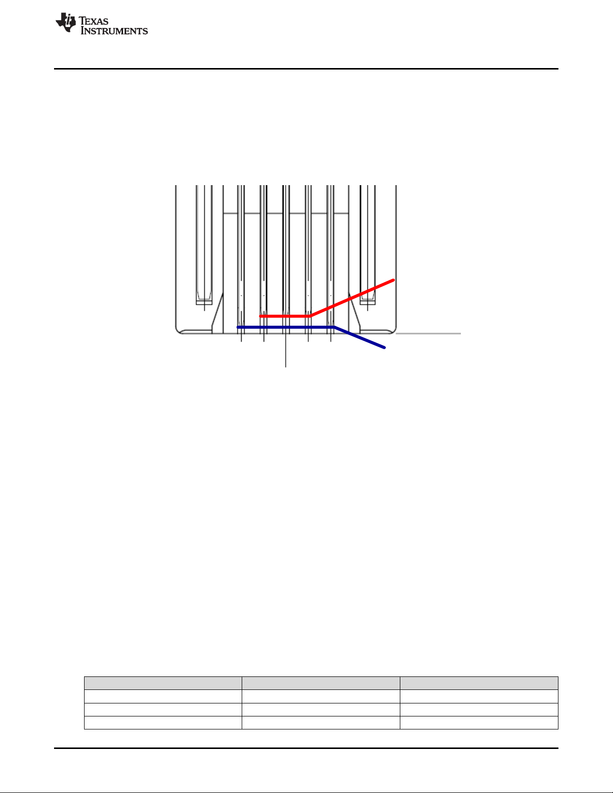
3.2 Slow Plug-in Event
As you insert a charger into the USB receptacle, the pins are configured so that the VBUS and GND pins
make contact first. This presents a problem as the BQ24392 (or any other charger detection IC) requires
access to the D+ D– lines to run detection. This is why the BQ24392 has a standard 130 ms de-bounce
time after VBUS valid to run the detection algorithm. This delay helps minimize the effects of the D+ D–
lines making contact after VBUS and GND.
Figure 2 is from the datasheet of a standard male micro-USB connector and shows how the data
connections (red line) are slightly recessed from the power connections (blue line).
BQ24392 Implementation Guidelines
Figure 2. Data Connections Recessed from Power Connections
However, in some cases the charger is inserted very slowly, causing the VBUS and GND to make contact
long before D+ D–. Due to this effect, there is no guaranteed detection time as the detection time can vary
based on how long it takes to insert the charger. If longer than 600 ms is taken to insert the charger into
the USB receptacle, the detection algorithm of the BQ24392 will timeout and instead of the charger being
detected as a DCP, it is now detected as a nonstandard charger (D+ and D– floating).
3.3 DBP Timer
The BQ24392 features a dead battery provision timer per the BC1.2 specification. Once a charger has
been detected and the GOOD_BAT pin is low, a dead battery timer is initiated. If the GOOD_BAT
continues to be LOW for 30 minutes (maximum of 45 minutes), charging is disabled and CHG_AL_N goes
into the High-Z state to indicate this. Toggling GOOD_BAT high after the DBP timer expires re-starts
detection and the DBP timer.
3.4 Using the BQ24932 GPIOS
3.4.1 CHG_AL and CHG_DET
The BQ24392 has 2 outputs, CHG_AL_N and CHG_DET, that the host can used to determine whether it
can charge and if it can charge at a low or high current. Table 2 demonstrates how these outputs should
be interpreted. CHG_AL_N is an open drain output and is active when the output of the pin is low.
CHG_DET is a push-pull output and is high in the active state.
Table 2. BQ24392 Outputs
CHG_AL_N CHG_DET
High-Z X Charging is not allowed
Low Low Low-current charging is allowed
Low High High-current charging is allowed
SLVUA61–April 2014 BQ24392EVM User's Guide
Submit Documentation Feedback
Copyright © 2014, Texas Instruments Incorporated
5
Page 6
BQ24392 Implementation Guidelines
The system must define what is meant by low- and high-current charging. If CHG_DET is high, a system
could try to draw 2 A, 1.5 A, or 1.0 A. If the system is trying to support > 1.5-A chargers, then the system
has to use a charger IC that is capable of monitoring the VBUS voltage as it tries to pull the higher current
values. If the voltage on VBUS starts to drop because that high of a current is supported then the system
has to back down on how much current it is trying to draw until it finds a stable state with VBUS not
dropping.
3.4.2 SW_OPEN
SW_OPEN is an open drain output that indicates whether the USB switches are opened or closed. In the
High-Z state the switches are open and in the active, or low state, the switches are closed. The host
should monitor this pin to know when the switches are closed or open.
3.4.3 GOOD_BAT
GOOD_BAT is used by the host controller to indicate the status of the battery to the BQ24392. This pin
affects the switch status for a SDP or CDP, and it also affects the DBP timer as discussed in the DBP
timer section.
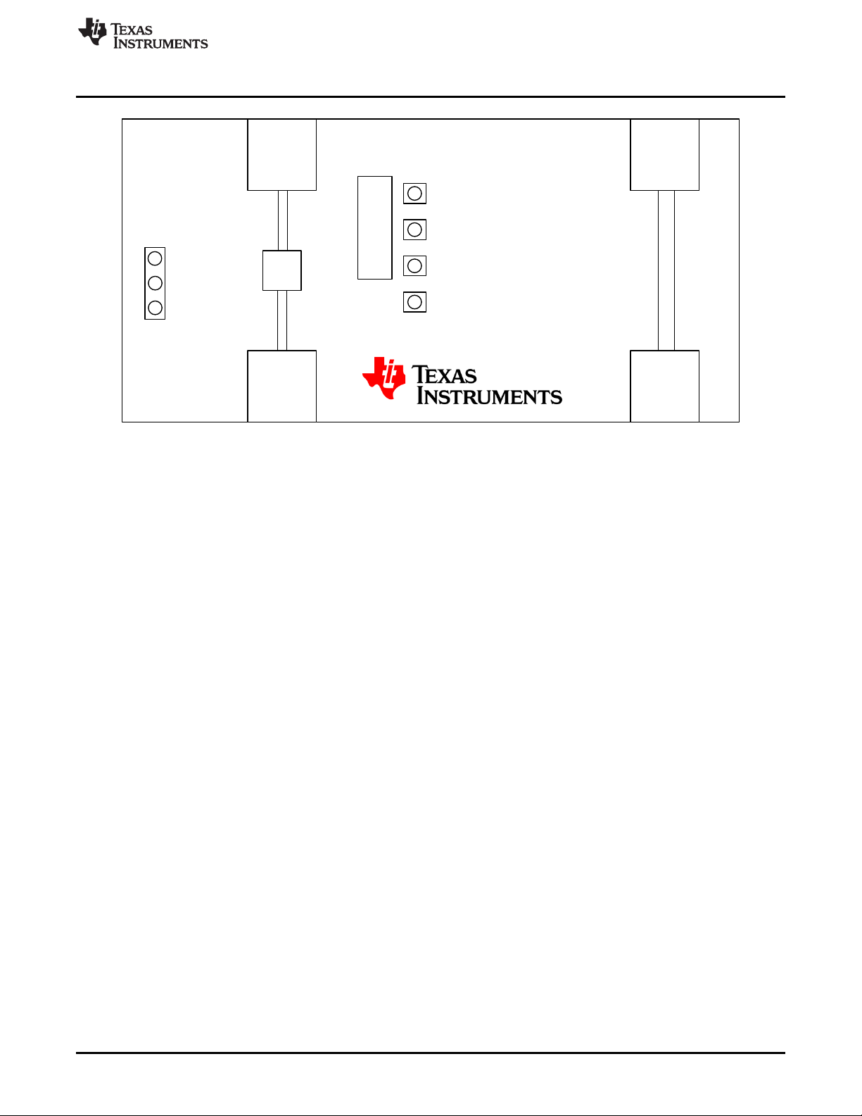
3.5 EVM Overview
The EVM for the BQ24392 is designed to be self-contained so no use of lab equipment is required to
evaluate the functionality of the battery charging detection or the USB communication capabilities.
However, there are test points available for more detailed analysis of the detection timings.
www.ti.com
3.5.1 Board Power
The EVM is fully supplied by VBUS from the charger or PC connected to the board with test points for
monitoring VBUS as a device is attached. The EVM also has an LED output indicating when VBUS is
present as depicted in the following figure:
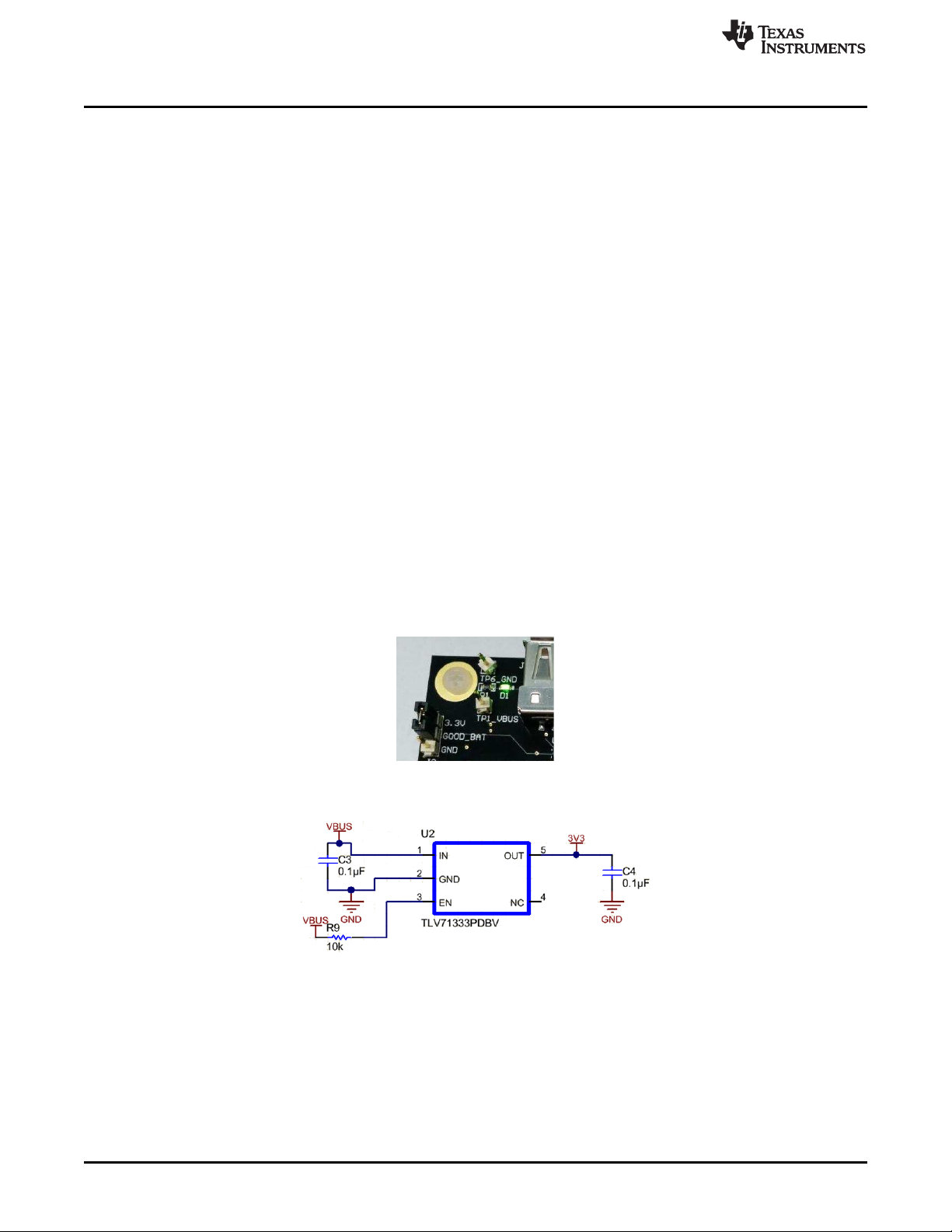
The EVM contains a 3.3-V output LDO for the SW_OPEN output and GOOD_BAT input as these pins
must not be connected to VBUS. Figure 3 is the schematic for this portion of the design.
Figure 3. Schematic for 3.3-V Output LDO
6
BQ24392EVM User's Guide SLVUA61–April 2014
Copyright © 2014, Texas Instruments Incorporated
Submit Documentation Feedback
Page 7
www.ti.com
3.5.2 GOOD_BAT Selection Jumper
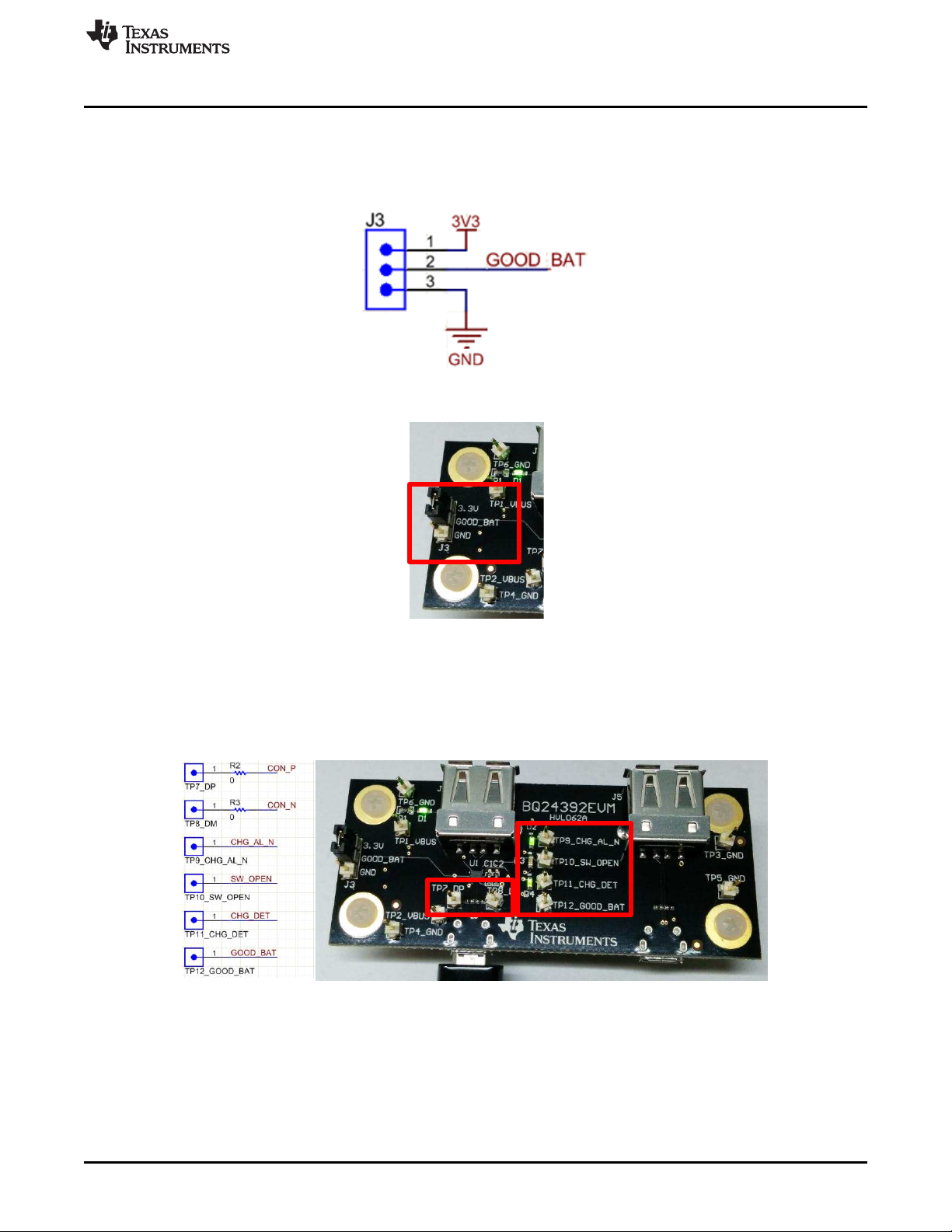
There is a 3-pin header (J3) on the EVM to select the GOOD_BAT input to be high or low. The jumper
positioning is fully labeled on the EVM itself for ease of use. Figure 4 and Figure 5 illustrate the schematic
and the EVM board labeling.
Figure 4. Schematic for GOOD_BAT Selection Header
BQ24392 Implementation Guidelines
3.5.3 Test Points
The EVM also contains test point for the 3 outputs, 1 input, and the D+ D– pins. Figure 6 shows the
schematic for these test points and the locations on the EVM.
Figure 5. GOOD_BAT Selection Header on EVM
Figure 6. Test Point Locations
SLVUA61–April 2014 BQ24392EVM User's Guide
Submit Documentation Feedback
Copyright © 2014, Texas Instruments Incorporated
7
Page 8

BQ24392 Implementation Guidelines
These test points also feature LED indicators that turn on when the output is active. That is, for CHG_DET
the LED turns on when the output is high. For CHG_AL_N and SW_OPEN, the LED turns on when the
output is low. Figure 7 is the schematic section for the LED output indicators.
3.5.4 USB Connections
The micro-USB connector (J2) is the common side of the BQ24392 and the standard-A USB connector
(J1) is the host side of the BQ24392.
There is also a through path on the board that can be used for testing. The connectors for the through
path are J4 and J5.
www.ti.com
Figure 7. LED Output Schematic
Figure 8. Device and USB Connections
3.6 BQ24392 Quick Start Evaluation
3.6.1 High-Current Chargers
High-current chargers include the following:
• BC1.2-compliant DCPs
• BC1.2-compliant CDPs
• Apple Chargers
• TomTom Chargers
8
BQ24392EVM User's Guide SLVUA61–April 2014
Copyright © 2014, Texas Instruments Incorporated
Submit Documentation Feedback
Page 9

www.ti.com
Table 3 shows the states the BQ24392 EVM has the output LEDs in after inserting any chargers from the
high-current charger list.
Output LED Status
CH_AL_N ON
CHG_DET ON
SW_OPEN OFF
Figure 9 is an image of the EVM after a high-current charger attachment.
BQ24392 Implementation Guidelines
Table 3. LED State After Inserting Charger
Figure 9. EVM After High-Current Charger Attached
3.6.2 Low-Current Chargers
Low-Current chargers include the following:
• SDP
• Nonstandard chargers with VBUS = 5 V and D+ D– floating
Table 4 shows the output status for different low current charger attachments, notice that the
GOOD_BAT input affects the SW_OPEN output for an SDP but not a nonstandard charger.
Table 4. Output Status for Different Low-Current Charger Attachments
Attachment GOOD_BAT LED Status
SDP LOW CHG_AL_N = ON
SDP High CHG_AL_N = ON
Nonstandard X CHG_AL_N = ON
CHG_DET = OFF
SW_OPEN = OFF
CHG_DET = OFF
SW_OPEN = ON
CHG_DET = OFF
SW_OPEN = OFF
SLVUA61–April 2014 BQ24392EVM User's Guide
Submit Documentation Feedback
Copyright © 2014, Texas Instruments Incorporated
9
Page 10

BQ24392 Implementation Guidelines
Figure 10. SDP with GOOD_BAT Low or Nonstandard Charger
Figure 11 shows how with an SDP, changing the GOOD_BAT input to high closes the switches and turns
on the SW_OPEN Output.
www.ti.com
10
Figure 11. SDP with GOOD_BAT = High
BQ24392EVM User's Guide SLVUA61–April 2014
Copyright © 2014, Texas Instruments Incorporated
Submit Documentation Feedback
Page 11

www.ti.com
3.6.3 USB Communication
It is also possible to communicate over USB through the BQ24392 EVM. By attaching an SDP to the
common side with GOOD_BAT = High, we can communicate to a USB thumb drive inserted into the
standard-A receptacle, see Figure 12 for an example.
BQ24392 Implementation Guidelines
Figure 12. USB Communication with Thumb Drive Through BQ24392
SLVUA61–April 2014 BQ24392EVM User's Guide
Submit Documentation Feedback
Copyright © 2014, Texas Instruments Incorporated
11
Page 12

Board Documentation
4 Board Documentation
This section contains the BOM, the EVM schematic, and the PCB layout drawings.
4.1 Bill of Materials
Table 5 lists the bill of materials for this EVM.
Designator Qty Value Description Package Reference Part Number
C1 1 1uF CAP, CERM, 1uF, 16V, +/-10%, X5R, 0603 0603 C0603C105K4PACTU
C2 1 0.1uF CAP, CERM, 0.1uF, 16V, +/-5%, X7R, 0603 0603 0603YC104JAT2A
C3, C4 2 0.1uF CAP, CERM, 0.1uF, 6.3V, +/-10%, X5R, 0402 0402 C1005X5R0J104K
D1, D2, D3, D4 4 Green LED, Green, SMD LED, GREEN, 0603 SML-LX0603GW-TR
H3, H4, H7, H8 4 Machine Screw, Round, #4-40 x 1/4, Nylon, Screw NY PMS 440 0025 PH
J1, J5 2 Connector, Receptacle, USB TYPE A, 4POS USB TYPE A 896-43-004-00-000000
J2, J4 2 Receptacle, Micro-USB-B, Right Angle, SMD Micro USB receptacle 105017-0001
J3 1 Header, TH, 100mil, 3x1, Gold plated, 230 mil 3x1 Header TSW-103-07-G-S
R1, R7 2 1.1k RES, 1.1k ohm, 5%, 0.1W, 0603 0603 CRCW06031K10JNEA
R2, R3, R4, R5 4 0 RES, 0 ohm, 5%, 0.063W, 0402 0402 CRCW04020000Z0ED
R6, R8 2 2.80k RES, 2.80k ohm, 1%, 0.1W, 0603 0603 CRCW06032K80FKEA
R9 1 10k RES,10k ohm, 5%, 0.1W, 0603 0603 CRCW060310K0JNEA
SH-J1 1 1x2 Shunt, 100mil, Gold plated, Black Shunt 969102-0000-DA
TP1_VBUS, TP2_VBUS, 12 Header, TH, 100mil, 1pos, Gold plated, 230 Testpoint TSW-101-07-G-S
TP3_GND, TP4_GND, mil above insulator
TP5_GND, TP6_GND,
TP7_DP, TP8_DM,
TP9_CHG_AL_N,
TP10_SW_OPEN,
TP11_CHG_DET,
TP12_GOOD_BAT
U1 1 Charger Detection Device with High Speed RSE0010A BQ24392RSE
U2 1 TLV7133PDBV IC, 150mA, Low IQ, Ultra Small LDO Voltage SOT TLV7133PDBV
www.ti.com
Table 5. bq24392 EVM Bill of Materials
Philips panhead
SMD CONNECTOR
RECEPTACLE 4POS
SMD
above insulator
USB Switch Battery Charger Specification
v1.2, RSE0010A
Reg.
12
BQ24392EVM User's Guide SLVUA61–April 2014
Copyright © 2014, Texas Instruments Incorporated
Submit Documentation Feedback
Page 13

SW_OPEN
1
DM_HOST
2
DP_HOST
3
CHG_AL_N
4
GOOD_BAT
5
GND
6
DP_CON
7
DM_CON
8
VBUS
9
CHG_DET
10
U1
BQ24392RSE
1
2
3
4
5
6
7
8
9
10
11
J2
1
2
3
4
5
6
7
8
9
10
11
J4
GND
GND
VBUS
VBUSVBUS
GND
GND
HOST_N
HOST_P
CON_P
CON_N
VBUS
GND
CHG_DET
CHG_AL_N
SW_OPEN
GOOD_BAT
Green
D4
Green
D3
GND
GND
GND
SW_OPENCHG_AL_N
VBUS 3V3
GND
CHG_DET
3V3
GOOD_BAT
GND
Jumper to select logic high or low for GOOD_BAT input
1
TP5_GND
1
TP4_GND
1
TP3_GND
1
TP6_GND
Through Path
1
TP9_CHG_AL_N
1
TP10_SW_OPEN
1
TP12_GOOD_BAT
CHG_AL_N
SW_OPEN
GOOD_BAT
1
TP11_CHG_DET
CHG_DET
GND
GND
1
TP8_DM
1
TP7_DP
2.80k
R6
1
TP2_VBUS
VBUS
0
R2
CON_N
CON_P
VBUS
1
D-
2
D+
3
GND
4
5
6
J5
VBUS
1
D-
2
D+
3
GND
4
5
6
J1
VBUS is Power input to Board
1
TP1_VBUS
GND
1.1k
R7
GND
VBUS
2.80k
R8
0
R3
Green
D2
Through_N
Through_P
IN
1
GND
2
EN3NC
4
OUT
5
U2
TLV71333PDBV
GND
VBUS
VBUS
3V3
GND
VBUS_Through_Path
0
R4
0
R5
Through_N
Through_P
10k
R9
1.1k
R1
Green
D1
0.1µF
C3
0.1µF
C4
1
2
3
J3
TSW-103-07-G-S
Resistors to match device USB path
1µFC10.1µF
C2
VBUS input range = 4.75 V to 5.25 V
Place de-coupling caps as close to VBUS pin as possible
Avoid placing de-coupling caps near DP/DM traces
LEDs are on if output is boolean True
Diode Forward Voltage = 2.2 V
VOL Max specified at IOL of 2 mA
www.ti.com
4.2 Schematic
Figure 13 illustrates the EVM schematic.
Board Documentation
SLVUA61–April 2014 BQ24392EVM User's Guide
Submit Documentation Feedback
Figure 13. BQ24392EVM Schematic
Copyright © 2014, Texas Instruments Incorporated
13
Page 14

Board Documentation
4.3 Board Layout
Figure 14 through Figure 19 illustrate the PCB layout for this EVM.
www.ti.com
Figure 14. Top Overlay
14
Figure 15. Top Layer
BQ24392EVM User's Guide SLVUA61–April 2014
Copyright © 2014, Texas Instruments Incorporated
Submit Documentation Feedback
Page 15

www.ti.com
Board Documentation
Figure 16. Ground Layer
Figure 17. Power Layer
SLVUA61–April 2014 BQ24392EVM User's Guide
Submit Documentation Feedback
Copyright © 2014, Texas Instruments Incorporated
15
Page 16

Board Documentation
www.ti.com
Figure 18. Bottom Layer
16
Figure 19. Bottom Overlay
BQ24392EVM User's Guide SLVUA61–April 2014
Copyright © 2014, Texas Instruments Incorporated
Submit Documentation Feedback
Page 17

www.ti.com
5 Board Stackup and Layout Guidelines
Figure 20 depicts the board stackup. All signal and plane layers are 1.4-mil thick.
• Core: FR-4
• Prepreg: FR-4
Figure 20. Board Stackup
6 Related Documentation
BQ24392 Charger Detection Device with High Speed USB Switch Battery Charger Specification v1.2
(SLIS146)
Board Stackup and Layout Guidelines
SLVUA61–April 2014 BQ24392EVM User's Guide
Submit Documentation Feedback
Copyright © 2014, Texas Instruments Incorporated
17
Page 18

ADDITIONAL TERMS AND CONDITIONS, WARNINGS, RESTRICTIONS, AND DISCLAIMERS FOR
EVALUATION MODULES
Texas Instruments Incorporated (TI) markets, sells, and loans all evaluation boards, kits, and/or modules (EVMs) pursuant to, and user
expressly acknowledges, represents, and agrees, and takes sole responsibility and risk with respect to, the following:
1. User agrees and acknowledges that EVMs are intended to be handled and used for feasibility evaluation only in laboratory and/or
development environments. Notwithstanding the foregoing, in certain instances, TI makes certain EVMs available to users that do not
handle and use EVMs solely for feasibility evaluation only in laboratory and/or development environments, but may use EVMs in a
hobbyist environment. All EVMs made available to hobbyist users are FCC certified, as applicable. Hobbyist users acknowledge, agree,
and shall comply with all applicable terms, conditions, warnings, and restrictions in this document and are subject to the disclaimer and
indemnity provisions included in this document.
2. Unless otherwise indicated, EVMs are not finished products and not intended for consumer use. EVMs are intended solely for use by
technically qualified electronics experts who are familiar with the dangers and application risks associated with handling electrical
mechanical components, systems, and subsystems.
3. User agrees that EVMs shall not be used as, or incorporated into, all or any part of a finished product.
4. User agrees and acknowledges that certain EVMs may not be designed or manufactured by TI.
5. User must read the user's guide and all other documentation accompanying EVMs, including without limitation any warning or
restriction notices, prior to handling and/or using EVMs. Such notices contain important safety information related to, for example,
temperatures and voltages. For additional information on TI's environmental and/or safety programs, please visit www.ti.com/esh or
contact TI.
6. User assumes all responsibility, obligation, and any corresponding liability for proper and safe handling and use of EVMs.
7. Should any EVM not meet the specifications indicated in the user’s guide or other documentation accompanying such EVM, the EVM
may be returned to TI within 30 days from the date of delivery for a full refund. THE FOREGOING LIMITED WARRANTY IS THE
EXCLUSIVE WARRANTY MADE BY TI TO USER AND IS IN LIEU OF ALL OTHER WARRANTIES, EXPRESSED, IMPLIED, OR
STATUTORY, INCLUDING ANY WARRANTY OF MERCHANTABILITY OR FITNESS FOR ANY PARTICULAR PURPOSE. TI SHALL
NOT BE LIABLE TO USER FOR ANY INDIRECT, SPECIAL, INCIDENTAL, OR CONSEQUENTIAL DAMAGES RELATED TO THE
HANDLING OR USE OF ANY EVM.
8. No license is granted under any patent right or other intellectual property right of TI covering or relating to any machine, process, or
combination in which EVMs might be or are used. TI currently deals with a variety of customers, and therefore TI’s arrangement with
the user is not exclusive. TI assumes no liability for applications assistance, customer product design, software performance, or
infringement of patents or services with respect to the handling or use of EVMs.
9. User assumes sole responsibility to determine whether EVMs may be subject to any applicable federal, state, or local laws and
regulatory requirements (including but not limited to U.S. Food and Drug Administration regulations, if applicable) related to its handling
and use of EVMs and, if applicable, compliance in all respects with such laws and regulations.
10. User has sole responsibility to ensure the safety of any activities to be conducted by it and its employees, affiliates, contractors or
designees, with respect to handling and using EVMs. Further, user is responsible to ensure that any interfaces (electronic and/or
mechanical) between EVMs and any human body are designed with suitable isolation and means to safely limit accessible leakage
currents to minimize the risk of electrical shock hazard.
11. User shall employ reasonable safeguards to ensure that user’s use of EVMs will not result in any property damage, injury or death,
even if EVMs should fail to perform as described or expected.
12. User shall be solely responsible for proper disposal and recycling of EVMs consistent with all applicable federal, state, and local
requirements.
Certain Instructions. User shall operate EVMs within TI’s recommended specifications and environmental considerations per the user’s
guide, accompanying documentation, and any other applicable requirements. Exceeding the specified ratings (including but not limited to
input and output voltage, current, power, and environmental ranges) for EVMs may cause property damage, personal injury or death. If
there are questions concerning these ratings, user should contact a TI field representative prior to connecting interface electronics including
input power and intended loads. Any loads applied outside of the specified output range may result in unintended and/or inaccurate
operation and/or possible permanent damage to the EVM and/or interface electronics. Please consult the applicable EVM user's guide prior
to connecting any load to the EVM output. If there is uncertainty as to the load specification, please contact a TI field representative. During
normal operation, some circuit components may have case temperatures greater than 60°C as long as the input and output are maintained
at a normal ambient operating temperature. These components include but are not limited to linear regulators, switching transistors, pass
transistors, and current sense resistors which can be identified using EVMs’ schematics located in the applicable EVM user's guide. When
placing measurement probes near EVMs during normal operation, please be aware that EVMs may become very warm. As with all
electronic evaluation tools, only qualified personnel knowledgeable in electronic measurement and diagnostics normally found in
development environments should use EVMs.
Agreement to Defend, Indemnify and Hold Harmless. User agrees to defend, indemnify, and hold TI, its directors, officers, employees,
agents, representatives, affiliates, licensors and their representatives harmless from and against any and all claims, damages, losses,
expenses, costs and liabilities (collectively, "Claims") arising out of, or in connection with, any handling and/or use of EVMs. User’s
indemnity shall apply whether Claims arise under law of tort or contract or any other legal theory, and even if EVMs fail to perform as
described or expected.
Safety-Critical or Life-Critical Applications. If user intends to use EVMs in evaluations of safety critical applications (such as life support),
and a failure of a TI product considered for purchase by user for use in user’s product would reasonably be expected to cause severe
personal injury or death such as devices which are classified as FDA Class III or similar classification, then user must specifically notify TI
of such intent and enter into a separate Assurance and Indemnity Agreement.
Page 19

RADIO FREQUENCY REGULATORY COMPLIANCE INFORMATION FOR EVALUATION MODULES
Texas Instruments Incorporated (TI) evaluation boards, kits, and/or modules (EVMs) and/or accompanying hardware that is marketed, sold,
or loaned to users may or may not be subject to radio frequency regulations in specific countries.
General Statement for EVMs Not Including a Radio
For EVMs not including a radio and not subject to the U.S. Federal Communications Commission (FCC) or Industry Canada (IC)
regulations, TI intends EVMs to be used only for engineering development, demonstration, or evaluation purposes. EVMs are not finished
products typically fit for general consumer use. EVMs may nonetheless generate, use, or radiate radio frequency energy, but have not been
tested for compliance with the limits of computing devices pursuant to part 15 of FCC or the ICES-003 rules. Operation of such EVMs may
cause interference with radio communications, in which case the user at his own expense will be required to take whatever measures may
be required to correct this interference.
General Statement for EVMs including a radio
User Power/Frequency Use Obligations: For EVMs including a radio, the radio included in such EVMs is intended for development and/or
professional use only in legally allocated frequency and power limits. Any use of radio frequencies and/or power availability in such EVMs
and their development application(s) must comply with local laws governing radio spectrum allocation and power limits for such EVMs. It is
the user’s sole responsibility to only operate this radio in legally acceptable frequency space and within legally mandated power limitations.
Any exceptions to this are strictly prohibited and unauthorized by TI unless user has obtained appropriate experimental and/or development
licenses from local regulatory authorities, which is the sole responsibility of the user, including its acceptable authorization.
U.S. Federal Communications Commission Compliance
For EVMs Annotated as FCC – FEDERAL COMMUNICATIONS COMMISSION Part 15 Compliant
Caution
This device complies with part 15 of the FCC Rules. Operation is subject to the following two conditions: (1) This device may not cause
harmful interference, and (2) this device must accept any interference received, including interference that may cause undesired operation.
Changes or modifications could void the user's authority to operate the equipment.
FCC Interference Statement for Class A EVM devices
This equipment has been tested and found to comply with the limits for a Class A digital device, pursuant to part 15 of the FCC Rules.
These limits are designed to provide reasonable protection against harmful interference when the equipment is operated in a commercial
environment. This equipment generates, uses, and can radiate radio frequency energy and, if not installed and used in accordance with the
instruction manual, may cause harmful interference to radio communications. Operation of this equipment in a residential area is likely to
cause harmful interference in which case the user will be required to correct the interference at its own expense.
FCC Interference Statement for Class B EVM devices
This equipment has been tested and found to comply with the limits for a Class B digital device, pursuant to part 15 of the FCC Rules.
These limits are designed to provide reasonable protection against harmful interference in a residential installation. This equipment
generates, uses and can radiate radio frequency energy and, if not installed and used in accordance with the instructions, may cause
harmful interference to radio communications. However, there is no guarantee that interference will not occur in a particular installation. If
this equipment does cause harmful interference to radio or television reception, which can be determined by turning the equipment off and
on, the user is encouraged to try to correct the interference by one or more of the following measures:
• Reorient or relocate the receiving antenna.
• Increase the separation between the equipment and receiver.
• Connect the equipment into an outlet on a circuit different from that to which the receiver is connected.
• Consult the dealer or an experienced radio/TV technician for help.
Industry Canada Compliance (English)
For EVMs Annotated as IC – INDUSTRY CANADA Compliant:
This Class A or B digital apparatus complies with Canadian ICES-003.
Changes or modifications not expressly approved by the party responsible for compliance could void the user’s authority to operate the
equipment.
Concerning EVMs Including Radio Transmitters
This device complies with Industry Canada licence-exempt RSS standard(s). Operation is subject to the following two conditions: (1) this
device may not cause interference, and (2) this device must accept any interference, including interference that may cause undesired
operation of the device.
Concerning EVMs Including Detachable Antennas
Under Industry Canada regulations, this radio transmitter may only operate using an antenna of a type and maximum (or lesser) gain
approved for the transmitter by Industry Canada. To reduce potential radio interference to other users, the antenna type and its gain should
be so chosen that the equivalent isotropically radiated power (e.i.r.p.) is not more than that necessary for successful communication.
This radio transmitter has been approved by Industry Canada to operate with the antenna types listed in the user guide with the maximum
permissible gain and required antenna impedance for each antenna type indicated. Antenna types not included in this list, having a gain
greater than the maximum gain indicated for that type, are strictly prohibited for use with this device.
Page 20

Canada Industry Canada Compliance (French)
Cet appareil numérique de la classe A ou B est conforme à la norme NMB-003 du Canada
Les changements ou les modifications pas expressément approuvés par la partie responsable de la conformité ont pu vider l’autorité de
l'utilisateur pour actionner l'équipement.
Concernant les EVMs avec appareils radio
Le présent appareil est conforme aux CNR d'Industrie Canada applicables aux appareils radio exempts de licence. L'exploitation est
autorisée aux deux conditions suivantes : (1) l'appareil ne doit pas produire de brouillage, et (2) l'utilisateur de l'appareil doit accepter tout
brouillage radioélectrique subi, même si le brouillage est susceptible d'en compromettre le fonctionnement.
Concernant les EVMs avec antennes détachables
Conformément à la réglementation d'Industrie Canada, le présent émetteur radio peut fonctionner avec une antenne d'un type et d'un gain
maximal (ou inférieur) approuvé pour l'émetteur par Industrie Canada. Dans le but de réduire les risques de brouillage radioélectrique à
l'intention des autres utilisateurs, il faut choisir le type d'antenne et son gain de sorte que la puissance isotrope rayonnée équivalente
(p.i.r.e.) ne dépasse pas l'intensité nécessaire à l'établissement d'une communication satisfaisante.
Le présent émetteur radio a été approuvé par Industrie Canada pour fonctionner avec les types d'antenne énumérés dans le manuel
d’usage et ayant un gain admissible maximal et l'impédance requise pour chaque type d'antenne. Les types d'antenne non inclus dans
cette liste, ou dont le gain est supérieur au gain maximal indiqué, sont strictement interdits pour l'exploitation de l'émetteur.
Mailing Address: Texas Instruments, Post Office Box 655303, Dallas, Texas 75265
Copyright © 2014, Texas Instruments Incorporated
spacer
Important Notice for Users of EVMs Considered “Radio Frequency Products” in Japan
EVMs entering Japan are NOT certified by TI as conforming to Technical Regulations of Radio Law of Japan.
If user uses EVMs in Japan, user is required by Radio Law of Japan to follow the instructions below with respect to EVMs:
1. Use EVMs in a shielded room or any other test facility as defined in the notification #173 issued by Ministry of Internal Affairs and
Communications on March 28, 2006, based on Sub-section 1.1 of Article 6 of the Ministry’s Rule for Enforcement of Radio Law of
Japan,
2. Use EVMs only after user obtains the license of Test Radio Station as provided in Radio Law of Japan with respect to EVMs, or
3. Use of EVMs only after user obtains the Technical Regulations Conformity Certification as provided in Radio Law of Japan with respect
to EVMs. Also, do not transfer EVMs, unless user gives the same notice above to the transferee. Please note that if user does not
follow the instructions above, user will be subject to penalties of Radio Law of Japan.
http://www.tij.co.jp
【無線電波を送信する製品の開発キットをお使いになる際の注意事項】 本開発キットは技術基準適合証明を受けておりません。 本製品の
ご使用に際しては、電波法遵守のため、以下のいずれかの措置を取っていただく必要がありますのでご注意ください。
1. 電波法施行規則第6条第1項第1号に基づく平成18年3月28日総務省告示第173号で定められた電波暗室等の試験設備でご使用いただく。
2. 実験局の免許を取得後ご使用いただく。
3. 技術基準適合証明を取得後ご使用いただく。。
なお、本製品は、上記の「ご使用にあたっての注意」を譲渡先、移転先に通知しない限り、譲渡、移転できないものとします
上記を遵守頂けない場合は、電波法の罰則が適用される可能性があることをご留意ください。
日本テキサス・インスツルメンツ株式会社
東京都新宿区西新宿6丁目24番1号
西新宿三井ビル
http://www.tij.co.jp
Texas Instruments Japan Limited
(address) 24-1, Nishi-Shinjuku 6 chome, Shinjuku-ku, Tokyo, Japan
Page 21

IMPORTANT NOTICE
Texas Instruments Incorporated and its subsidiaries (TI) reserve the right to make corrections, enhancements, improvements and other
changes to its semiconductor products and services per JESD46, latest issue, and to discontinue any product or service per JESD48, latest
issue. Buyers should obtain the latest relevant information before placing orders and should verify that such information is current and
complete. All semiconductor products (also referred to herein as “components”) are sold subject to TI’s terms and conditions of sale
supplied at the time of order acknowledgment.
TI warrants performance of its components to the specifications applicable at the time of sale, in accordance with the warranty in TI’s terms
and conditions of sale of semiconductor products. Testing and other quality control techniques are used to the extent TI deems necessary
to support this warranty. Except where mandated by applicable law, testing of all parameters of each component is not necessarily
performed.
TI assumes no liability for applications assistance or the design of Buyers’ products. Buyers are responsible for their products and
applications using TI components. To minimize the risks associated with Buyers’ products and applications, Buyers should provide
adequate design and operating safeguards.
TI does not warrant or represent that any license, either express or implied, is granted under any patent right, copyright, mask work right, or
other intellectual property right relating to any combination, machine, or process in which TI components or services are used. Information
published by TI regarding third-party products or services does not constitute a license to use such products or services or a warranty or
endorsement thereof. Use of such information may require a license from a third party under the patents or other intellectual property of the
third party, or a license from TI under the patents or other intellectual property of TI.
Reproduction of significant portions of TI information in TI data books or data sheets is permissible only if reproduction is without alteration
and is accompanied by all associated warranties, conditions, limitations, and notices. TI is not responsible or liable for such altered
documentation. Information of third parties may be subject to additional restrictions.
Resale of TI components or services with statements different from or beyond the parameters stated by TI for that component or service
voids all express and any implied warranties for the associated TI component or service and is an unfair and deceptive business practice.
TI is not responsible or liable for any such statements.
Buyer acknowledges and agrees that it is solely responsible for compliance with all legal, regulatory and safety-related requirements
concerning its products, and any use of TI components in its applications, notwithstanding any applications-related information or support
that may be provided by TI. Buyer represents and agrees that it has all the necessary expertise to create and implement safeguards which
anticipate dangerous consequences of failures, monitor failures and their consequences, lessen the likelihood of failures that might cause
harm and take appropriate remedial actions. Buyer will fully indemnify TI and its representatives against any damages arising out of the use
of any TI components in safety-critical applications.
In some cases, TI components may be promoted specifically to facilitate safety-related applications. With such components, TI’s goal is to
help enable customers to design and create their own end-product solutions that meet applicable functional safety standards and
requirements. Nonetheless, such components are subject to these terms.
No TI components are authorized for use in FDA Class III (or similar life-critical medical equipment) unless authorized officers of the parties
have executed a special agreement specifically governing such use.
Only those TI components which TI has specifically designated as military grade or “enhanced plastic” are designed and intended for use in
military/aerospace applications or environments. Buyer acknowledges and agrees that any military or aerospace use of TI components
which have not been so designated is solely at the Buyer's risk, and that Buyer is solely responsible for compliance with all legal and
regulatory requirements in connection with such use.
TI has specifically designated certain components as meeting ISO/TS16949 requirements, mainly for automotive use. In any case of use of
non-designated products, TI will not be responsible for any failure to meet ISO/TS16949.
Products Applications
Audio www.ti.com/audio Automotive and Transportation www.ti.com/automotive
Amplifiers amplifier.ti.com Communications and Telecom www.ti.com/communications
Data Converters dataconverter.ti.com Computers and Peripherals www.ti.com/computers
DLP® Products www.dlp.com Consumer Electronics www.ti.com/consumer-apps
DSP dsp.ti.com Energy and Lighting www.ti.com/energy
Clocks and Timers www.ti.com/clocks Industrial www.ti.com/industrial
Interface interface.ti.com Medical www.ti.com/medical
Logic logic.ti.com Security www.ti.com/security
Power Mgmt power.ti.com Space, Avionics and Defense www.ti.com/space-avionics-defense
Microcontrollers microcontroller.ti.com Video and Imaging www.ti.com/video
RFID www.ti-rfid.com
OMAP Applications Processors www.ti.com/omap TI E2E Community e2e.ti.com
Wireless Connectivity www.ti.com/wirelessconnectivity
Mailing Address: Texas Instruments, Post Office Box 655303, Dallas, Texas 75265
Copyright © 2014, Texas Instruments Incorporated
Page 22

Mouser Electronics
Authorized Distributor
Click to View Pricing, Inventory, Delivery & Lifecycle Information:
Texas Instruments:
BQ24392EVM
 Loading...