

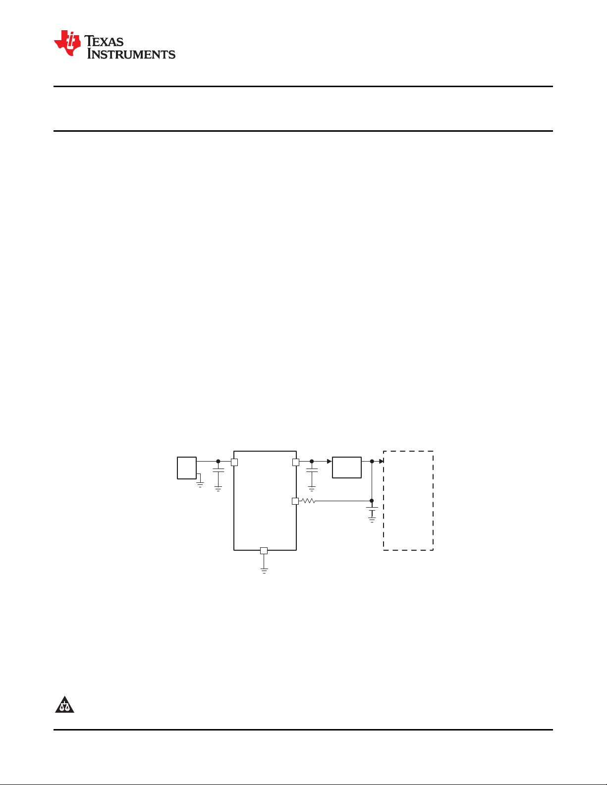
1
8
VDC
GND
1 Fm
IN
OUT
VBAT
bq24380
1 Fm
Charging
Circuit
6
SYSTEM
AC Adapter
2
VSS
bq24380
bq24381
bq24382
www.ti.com
......................................................................................................................................................... SLUS805B – APRIL 2008 – REVISED MARCH 2009
Overvoltage and Overcurrent Protection IC and Li+ Charger Front-End Protection IC With
LDO Mode
1
FEATURES DESCRIPTION
2
• Input Overvoltage Protection
• Accurate Battery Overvoltage Protection
• Output Short-Circuit Protection
• Soft-Start to Prevent Inrush Currents
• Soft-Stop to Prevent Voltage Spikes regulator, maintaining a 5.5-V (bq24380) or 5-V
• 30-V Maximum Input Voltage
• Supports up to 1.7-A Load Current
• Thermal Shutdown
• Enable Function
• Fault Status Indication
• Small 2 mm × 2 mm 8-Pin SON Package
APPLICATIONS
• Smart Phones, Mobile Phones
• PDAs
• MP3 Players
• Low-Power Handheld Devices
The bq2438x family are charger front-end integrated
circuits designed to provide protection to Li-ion
batteries from failures of the charging circuitry. The IC
continuously monitors the input voltage and the
battery voltage. The device operates like a linear
(bq24381, bq24382) output with input voltages up to
the Input overvoltage threshold. During input
overvoltage conditions, the IC immediately turns off
the internal pass FET disconnecting the charging
circuitry from the damaging input source. Additionally,
if the battery voltage rises to unsafe levels while
charging, power is removed from the system. The IC
checks for short-circuit or overload conditions at its
output when turning the pass FET on, and if it finds
unsafe conditions, it switches off, and then rechecks
the conditions. Additionally, the IC also monitors its
die temperature and switches off if it exceeds 140 ° C.
When the IC is controlled by a processor, the IC
provides status information about fault conditions to
the host.
APPLICATION SCHEMATIC
1
Please be aware that an important notice concerning availability, standard warranty, and use in critical applications of Texas
Instruments semiconductor products and disclaimers thereto appears at the end of this data sheet.
2 PowerPAD is a trademark of Texas Instruments.
PRODUCTION DATA information is current as of publication date.
Products conform to specifications per the terms of the Texas
Instruments standard warranty. Production processing does not
necessarily include testing of all parameters.
Copyright © 2008 – 2009, Texas Instruments Incorporated
bq24380
bq24381
bq24382
SLUS805B – APRIL 2008 – REVISED MARCH 2009 .........................................................................................................................................................
These devices have limited built-in ESD protection. The leads should be shorted together or the device placed in conductive foam
during storage or handling to prevent electrostatic damage to the MOS gates.
ORDERING INFORMATION
DEVICE V
bq24380 6.3 V 5.5 V 2mm x 2mm SON CFE
bq24381 7.1 V 5 V 2mm x 2mm SON CFW
bq24382 10.5 V 5 V 2mm x 2mm SON OBE
(1) For the most current package and ordering information, see the Package Option Addendum at the end
of this document, or see the TI Web site at www.ti.com .
OVP
V
O(REG)
PACKAGE
(1)
MARKING
www.ti.com
ABSOLUTE MAXIMUM RATINGS
(1)
over operating free-air temperature range (unless otherwise noted)
VALUE UNIT
IN (with respect to VSS) – 0.3 to 30 V
V
I
I
max Output source current OUT 2 A
OUT
T
J
T
stg
(1) Stresses beyond those listed under absolute maximum ratings may cause permanent damage to the device. These are stress ratings
only, and functional operation of the device at these or any other conditions beyond those indicated under recommended operating
conditions is not implied. Exposure to absolute-maximum-rated conditions for extended periods may affect device reliability. All voltage
values are with respect to the network ground terminal unless otherwise noted.
Input voltage OUT (with respect to VSS) – 0.3 to 12 V
FAULT, CE, VBAT (with respect to VSS) – 0.3 to 7 V
Output sink current FAULT 15 mA
Junction temperature – 40 to 150 ° C
Storage temperature – 65 to 150 ° C
DISSIPATION RATINGS
PACKAGE R
DSG 5 ° C/W 75 ° C/W
θ JC
R
θ JA
RECOMMENDED OPERATING CONDITIONS
MIN MAX UNIT
V
I
I
O
T
J
IN voltage range 3.3 30 V
Current, OUT pin 1.7 A
Junction temperature -40 125 ° C
2 Submit Documentation Feedback Copyright © 2008 – 2009, Texas Instruments Incorporated
Product Folder Link(s): bq24380 bq24381 bq24382
bq24380
bq24381
bq24382
www.ti.com
ELECTRICAL CHARACTERISTICS
Over junction temperature range -40 ° C ≤ TJ≤ 125 ° C and recommended supply voltage (unless otherwise noted)
IN
UVLO CE = LO or HI, VIN: 0 V → 3 V 2.5 2.8 V
V
hys(UVLO)
t
DGL(PGOOD)
I
DD
I
STDBY
INPUT-TO-OUTPUT CHARACTERISTICS
V
DO
I
OFF
INPUT OVERVOLTAGE PROTECTION
V
O(REG)
V
OVP
V
hys(OVP)
t
PD(OVP)
t
REC(OVP)
OUTPUT SHORT-CIRCUIT PROTECTION (only at start-up)
I
O(SC)
t
REC(SC)
BATTERY OVERVOLTAGE PROTECTION
BV
OVP
V
hys(BVovp)
I
(VBAT)
t
DGL(BVovp)
THERMAL PROTECTION
T
J(OFF)
T
J(OFF-HYS)
LOGIC LEVELS ON CE
V
IL
V
IH
I
IL
I
IH
LOGIC LEVELS ON FAULT
V
OL
I
lkg
(1) Not tested. Specified by design
......................................................................................................................................................... SLUS805B – APRIL 2008 – REVISED MARCH 2009
PARAMETER TEST CONDITIONS MIN TYP MAX UNIT
Undervoltage lock-out, input power
detected threshold
Hysteresis on UVLO CE = LO or HI, VIN: 3 V → 0 V 200 300 mV
Deglitch time, input power detected status 8 ms
Operating current bq24381 300 µ A
CE = LO or HI. Time measured from
VIN0 V → 5 V 1- µ s rise-time
CE = LO, no load on OUT pin,
VIN= 5 V
bq24380 250
bq24382 300
Standby current CE = HI, VIN= 5.5 V 100 µ A
Dropout voltage IN to OUT CE = LO, VIN= 5 V, I
= 1 A 280 mV
(OUT)
Q1 off-state leakage current CE = HI, VIN= 5.5 V 10 µ A
bq24380 5.3 5.5 5.7
Output voltage CE = LO, VIN= 6 V bq24381 4.8 5 5.2 V
bq24382 4.8 5 5.2
bq24380 6.1 6.3 6.5
Input overvoltage protection threshold CE = LO, VIN: 5 V → 8 V bq24831 6.88 7.1 7.31 V
bq24382 10.17 10.5 10.83
CE = LO or HI, VIN: 7 V → 5 V bq24380 25 110
Hysteresis on OVP bq24831 25 120 mV
(1)
Input OV propagation delay VIN: 5 V → 10 V 200 ns
Recovery time from input overvoltage condition 8 ms
Short-circuit detection threshold 3 V < VIN< V
CE = LO or HI, VIN: 8 V → 5 V
CE = LO. Time measured from
VIN: 7 V → 5 V, 1- µ s fall-time
- V
OVP
hys(OVP)
bq24382 150 300
1.3 1.5 1.7 A
Retry interval if short-circuit detected 64 ms
Battery overvoltage protection threshold VIN> 4.5 V, CE = LO 4.3 4.35 4.4 V
Hysteresis on BV
(OVP)
VIN> 4.5 V, CE = LO 200 320 mV
Input bias current on VBAT pin TJ= 25 ° C 10 nA
VIN> 4.5 V, CE = LO, Time measured from
Deglitch time, battery overvoltage detected V
rising from 4.1 V to 4.4 V to FAULT 176 µ s
VSAT
going low.
Thermal shutdown temperature 140 150 ° C
Thermal shutdown hysteresis 20 ° C
Logic LOW input voltage 0 0.4 V
Logic HIGH input voltage 1.4 V
VCE= 1.8 V 15 µ A
Output LOW voltage I
Off-state leakage current, HI-Z V
= 5 mA 0.2 V
SINK
= 5 V 10 µ A
FAULT
1 µ A
Copyright © 2008 – 2009, Texas Instruments Incorporated Submit Documentation Feedback 3
Product Folder Link(s): bq24380 bq24381 bq24382
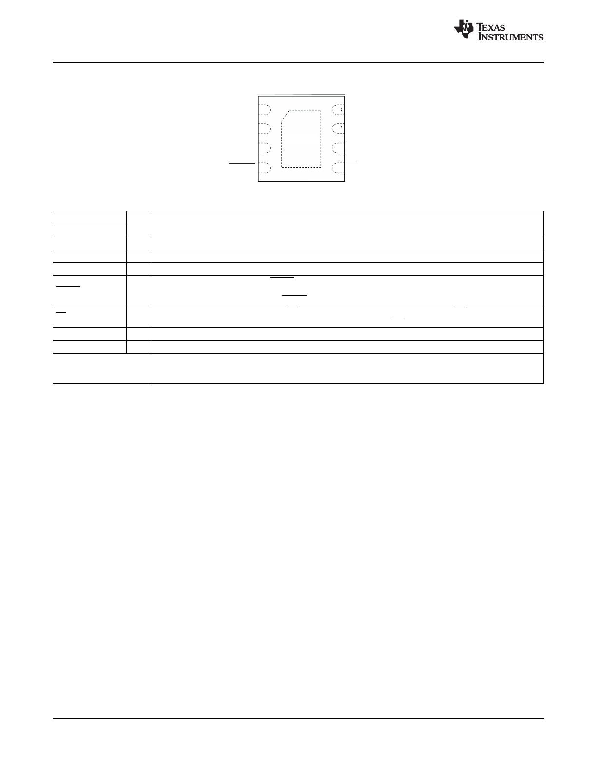
IN
VSS
NC
FAULT
OUT
NC
VBAT
CE
bq2438x
1
2
3
4
8
7
6
5
bq24380
bq24381
bq24382
SLUS805B – APRIL 2008 – REVISED MARCH 2009 .........................................................................................................................................................
DEVICE INFORMATION
TERMINAL FUNCTIONS
TERMINAL
NAME NO.
IN 1 I Input power, connected to external DC supply. Bypass IN to VSS with a ceramic capacitor (1 µ F minimum)
VSS 2 – Ground terminal. Connect to the thermal pad and to the ground rail of the circuit.
NC 3, 7 Do not connect to any external circuits. These pins may have internal connections used for test purposes.
FAULT 4 O off due to input overvoltage or output short-circuit conditions, an overtemperature condition, or because the
CE 5 I
VBAT 6 I Battery voltage sense input. Connected to pack positive terminal through a 100-k Ω resistor.
OUT 8 O Output terminal to the charging system. Bypass OUT to VSS with a ceramic capacitor (1 µ F minimum)
Thermal PAD potential as the VSS pin on the printed circuit board. Do not use the thermal pad as the primary ground input
I/O DESCRIPTION
Open-drain device status output. FAULT is pulled to VSS internally when the input pass FET has been turned
battery voltage is outside safe limits. FAULT is high impedance during normal operation.
Active-low chip enable input. Connect CE = HI to turn the input pass FET off. Connect CE = LOW to turn the
internal pass FET on and connect the input to the charging circuitry. CE is Internally pulled down, ~200 k Ω .
The thermal pad is electrically connected to VSS internally. The thermal pad must be connected to the same
for the device. VSS pin must be connected to ground at all times.
www.ti.com
4 Submit Documentation Feedback Copyright © 2008 – 2009, Texas Instruments Incorporated
Product Folder Link(s): bq24380 bq24381 bq24382
V
2V/div
FAULT
V
500mV/div
OUT
t-Time-2ms/div
V
5V/div
IN
V
2V/div
IN
V
2V/div
OUT
I
500mA/div
OUT
R =6.6
OUT
W
t-Time-2ms/div
V
2V/div
IN
V
2V/div
OUT
V
2V/div
FAULT
t-Time-200ms/div
V
2V/div
IN
V
2V/div
OUT
V
2V/div
FAULT
V =6Vto9Vstep
IN
t-Time-5 s/divm
V
5V/div
IN
V
2V/div
OUT
V =10Vto6Vstep
IN
V
2V/div
FAULT
t-Time-2ms/div
V
5V/div
IN
V
5V/div
OUT
I
1 A/div
OUT
V
2V/div
FAULT
t-Time-5ms/div
bq24380
bq24381
bq24382
www.ti.com
......................................................................................................................................................... SLUS805B – APRIL 2008 – REVISED MARCH 2009
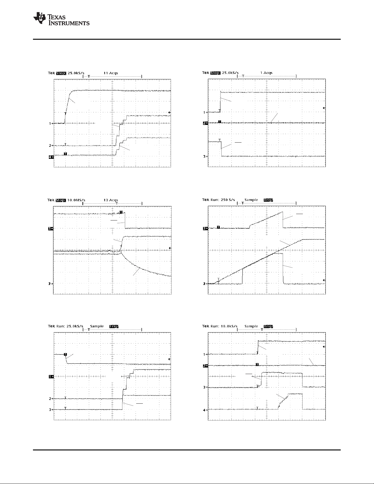
TYPICAL CHARACTERISTICS
NORMAL POWER-ON
SHOWING SOFT-START (bq24380) OVP at POWER-ON
Figure 1. Figure 2.
OVP RESPONSE for INPUT STEP (bq24380) SLOW INPUT RAMPINTO OVP EVENT (bq24380)
Figure 3. Figure 4.
RECOVERY FROM OVP (bq24380) POWER UP INTO SHORT CIRCUIT
Copyright © 2008 – 2009, Texas Instruments Incorporated Submit Documentation Feedback 5
Figure 5. Figure 6.
Product Folder Link(s): bq24380 bq24381 bq24382
V
2V/div
OUT
V =3.8Vto4.5Vstep
BAT
V
2V/div
FAULT
t-Time-50 s/divm
V
1V/div
BAT
V
5V/div
IN
V
500mV/div
OUT
I
1 A/div
OUT
t-Time-20 s/divm
2.40
2.45
2.50
2.55
2.60
2.65
2.70
2.75
-40 -15 10 35 60 85 110 135
T -Free-AirTemperature-°C
A
UVLO-UndervoltageLockout-V
V Rising
IN
V Falling
IN
50
90
130
170
210
250
-40 -15 10 35 60 85 110 135
DROPOUTVOLTAGE-mV
T -Free-AirTemperature-°C
A
I =1 A
OUT
V =5V
IN
V =4V
IN
6.0
6.4
6.8
7.0
7.2
7.4
–40 –15 10 35 60 85 110 135
V – Threshold – V
OVP
T – Free-AirTemperature – °C
A
6.6
6.2
V Rising
IN
V Rising
IN
V Falling
IN
bq24380
bq24381
V Falling
IN
4.90
5.00
5.10
5.20
5.30
5.40
5.50
5.60
–40 –15
10 35 60 85
110 135
V – OutputVoltage
–
V
OUT(REG)
T – Free-AirTemperature – °C
A
bq24380
bq24381
bq24380
bq24381
bq24382
SLUS805B – APRIL 2008 – REVISED MARCH 2009 .........................................................................................................................................................
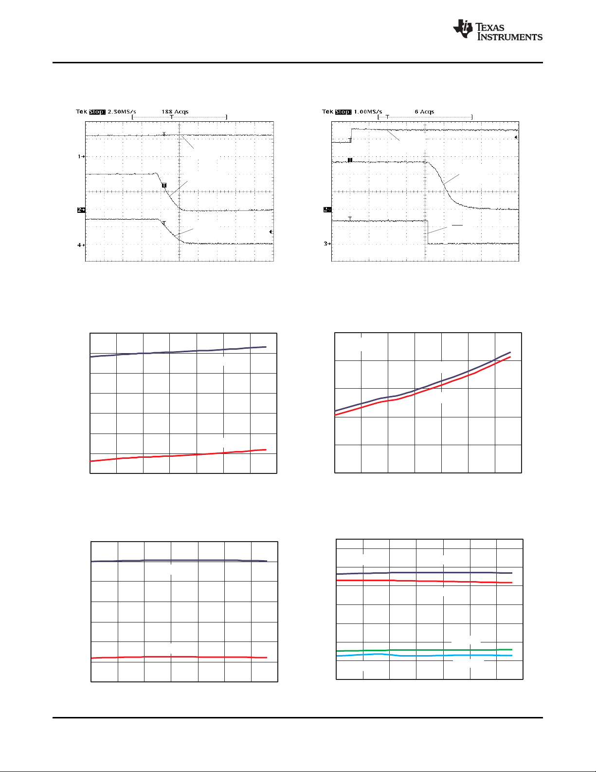
TYPICAL CHARACTERISTICS (continued)
SOFT-STOP DURING OCP EVENT (bq24380) BATTERY OVP EVENT (bq24380)
Figure 7. Figure 8.
www.ti.com
UVLO DROPOUT VOLTAGE
vs vs
FREE-AIR TEMPERATURE FREE-AIR TEMPERATURE
Figure 9. Figure 10.
OUTPUT VOLTAGE REGULATION, V
vs vs
O(REG)
FREE-AIR TEMPERATURE FREE-AIR TEMPERATURE
OVP THRESHOLD
6 Submit Documentation Feedback Copyright © 2008 – 2009, Texas Instruments Incorporated
Figure 11. Figure 12.
Product Folder Link(s): bq24380 bq24381 bq24382

4.05
4.10
4.15
4.20
4.25
4.30
4.35
4.40
-40 -15 10 35 60 85 110 135
V
-Threshold-V
BOVP
T -Free-AirTemperature-°C
A
V Rising
BAT
V Falling
BAT
0
5
10
15
20
25
-40 -15 10 35 60 85 110 135
I -BatLeakageCurrent-nA
Ikg
T -Free-AirTemperature-°C
A
0
100
200
300
400
500
600
700
800
900
1000
0 5 10 15 20 25 30
V – InputVoltage – V
IN
I – SupplyCurrent – A
CC
m
ICEnabled
ICDisabled
V
O(REG)
0
100
200
300
400
500
600
700
800
900
1000
0 5 10 15 20 25 30
V – InputVoltage – V
IN
I – SupplyCurrent – A
CC
m
V
O(REG)
ICEnabled
ICDisabled
bq24380
bq24381
bq24382
www.ti.com
......................................................................................................................................................... SLUS805B – APRIL 2008 – REVISED MARCH 2009
TYPICAL CHARACTERISTICS (continued)
OVP THRESHOLD, V
vs vs
BOVP
LEAKAGE CURRENT (VBAT PIN)
FREE-AIR TEMPERATURE FREE-AIR TEMPERATURE
Figure 13. Figure 14.
SUPPLY CURRENT SUPPLY CURRENT
vs vs
INPUT VOLTAGE (bq24380) INPUT VOLTAGE (bq24381)
Figure 15. Figure 16.
Copyright © 2008 – 2009, Texas Instruments Incorporated Submit Documentation Feedback 7
Product Folder Link(s): bq24380 bq24381 bq24382

1
8
VDC
GND
1 Fm
IN
OUT
VBAT
bq24380
1 Fm
Charging
Circuit
6
SYSTEM
AC Adapter
2
VSS
4
5
FAULT
CE
R
PU
100kW
47kW
47kW
R
FAULT
47kW
R
CE
R
BAT
1. Short-circuitduringstart-up
2. Normalstart-upcondition
3. Batteryovervoltageevent
4. V
UVLO
< VIN< V
OREG
-- V
OUT
tracksV
IN
5. Inputovervoltageevent
6. InputbelowUVLO
7. High-currenteventduringnormaloperation
t
CHK(SC)
t
SStart
t
SStop
t
REC(SC)
t
SStart
t
DGL(BVOVP)
t
PD(OVP)
t
DGL(PGOOD)
t
REC(OVP)
5
4
2
4
6
7
22
1
3
Input
Voltage
Output
Voltage
CE
UVLO
FAULT
Output
Current
Battery
Voltage
V
OVP
V
OVP hys(OVP)
-V
V
O(REG)
V
O(REG)
I
O(SC)
BV
BV -V
(OVP)
(OVP) hys(BVOVP)
bq24380
bq24381
bq24382
SLUS805B – APRIL 2008 – REVISED MARCH 2009 .........................................................................................................................................................
Figure 17. Typical Application Circuit
www.ti.com
8 Submit Documentation Feedback Copyright © 2008 – 2009, Texas Instruments Incorporated
Figure 18. Timing Diagram
Product Folder Link(s): bq24380 bq24381 bq24382

bq24380
bq24381
bq24382
www.ti.com
The bq2438x is a highly integrated circuit designed to provide protection to Li-ion batteries from failures of the
charging circuit and the input source. The IC continuously monitors the input voltage and the battery voltage. The
device operates like a linear regulator, maintaining a 5.5-V (bq24380) or 5-V (bq24381, bq24382) output with
input voltages up to the input overvoltage threshold (V
pass FET and disconnects the system from input power. Additionally, if the battery voltage rises above 4.35 V,
the IC switches off the pass FET, removing the power from the system until the battery voltage falls to safe
levels. The IC also monitors its die temperature and switches the pass FET off if it exceeds 140 ° C.
The IC can be controlled by a processor, and also provides status information about fault conditions to the host.
POWER DOWN
The device remains in power-down mode when the input voltage at the IN pin is below the undervoltage
threshold (UVLO) of 2.8 V. The FET connected between the IN and OUT pins is off, and the status output,
FAULT, is set to HI-Z.
POWER ON RESET
The device resets when the input voltage at the IN pin exceeds the UVLO threshold. During power-on reset, the
IC waits for duration t
voltage are within operation limits, the pass FET is turned ON. The IC has a soft-start feature to control the
inrush current. The soft-start minimizes the ringing at the input due to the resonant circuit formed by the parasitic
inductance of the adapter cable and the input bypass capacitor. During the soft-start time, t
is stepped up in 8 equal steps every 625 µ s. Each step is 1/8 of the I
the IC samples the load current. If the load current exceeds I
Startup Short-Circuit Protection section for details. If no overcurrent event is measured, the current monitoring
circuitry is disabled for normal operation.
In the event a short-circuit is detected at power-on, to prevent the input voltage from spiking up when the pass
FET is switched off (due to the inductance of the input cable), The pass FET is turned off by gradually reducing
its gate-drive, resulting in a soft-stop (t
......................................................................................................................................................... SLUS805B – APRIL 2008 – REVISED MARCH 2009
DETAILED FUNCTIONAL DESCRIPTION
). If the input voltage exceeds V
OVP
DGL(PGOOD)
for the input voltage to stabilize. If, after t
O(SC)
, the IC initiates short circuit protection. See the
O(SC)
).
SStop
DGL(PGOOD)
. After the soft-start sequence is over,
, the input voltage and battery
, the IC shuts off the
OVP
, the current limit
SStart
DETAILED FUNCTIONAL DESCRIPTION
The device continuously monitors the input voltage and the battery voltage as described in detail below:
Input Overvoltage Protection
The OUT output of the bq2438x operates similar to a linear regulator. While the input voltage is less than
V
pass FET). When the input voltage is greater than V
voltage is regulated to V
input voltage is increased above V
circuitry connected to OUT. The FAULT output is then asserted low. When the input voltage drops below V
V
ensures that the input supply has stabilized. The condition 5 in Figure 18 illustrates an input overvoltage event.
Battery Overvoltage Protection
The battery overvoltage threshold BV
illustrates a battery overvoltage event. If the battery voltage exceeds the BV
t
(using the soft-start sequence) once the battery voltage drops to BV
Thermal Protection
If the junction temperature of the device exceeds T
asserted low. The FET is turned on when the junction temperature falls below T
, and above the UVLO, the output voltage tracks the input voltage (less the drop caused by R
O(REG)
. V
O(REG)
hys(OVP)
DGL(BVovp)
(but is still above UVLO), the pass FET is turned on after a deglitch time of t
, the pass FET is turned off (using soft-stop), and FAULT is asserted low. The pass FET is turned on
is 5.5 V for the bq24380, and 5 V for the bq24381 and bq24382. If the
O(REG)
, the internal pass FET is turned off, removing power from the charging
OVP
is internally set to 4.35 V for the bq2438x. Condition 3 in Figure 18
OVP
(plus the R
O(REG)
OVP
, the pass FET is turned off, and the FAULT output is
J(OFF)
drop) and less than V
DS(on)
– V
hys(BVovp)
J(OFF)
OVP
.
OVP
REC(OVP)
. The deglitch time
threshold for longer than
– T
J(OFF-HYS)
.
DS(on)
, the output
of the
–
OVP
Copyright © 2008 – 2009, Texas Instruments Incorporated Submit Documentation Feedback 9
Product Folder Link(s): bq24380 bq24381 bq24382

bq24380
bq24381
bq24382
SLUS805B – APRIL 2008 – REVISED MARCH 2009 .........................................................................................................................................................
Start-Up Short-Circuit Protection
The bq2438x features overload current protection during start-up. The condition 1 in Figure 18 illustrates start-up
into an overload condition. If after the eight soft-start steps are complete, and the current limit is exceeded, the IC
initiates a short-circuit check timer (t
t
CHK(SC)
timer expires and the current remains clamped by the current limit, the internal pass FET is turned off
using the soft-stop method, FAULT is pulled low and the t
). During this check, the current is clamped to I
CHK(SC)
REC(SC)
timer begins. Once the t
O(SC)
REC(SC)
FAULT becomes high impedance and the soft-start sequence restarts. The device repeats the start/fail sequence
until the overload condition is removed. Once the overload condition is removed, the current limit circuitry is
disabled and the device enters normal operation. Additionally, if the current is not limited after the completion of
the soft-start sequence, the t
CHK(SC)
timer does not start and the current limit circuitry is disabled for normal
operation.
Enable Function
The IC has an enable pin which is used to enable and disable the device. Connect the CE pin high to turn off the
internal pass FET. Connect the CE pin low to turn on the internal pass FET and enter the start-up routine. The
CE pin has an internal pulldown resistor and can be left unconnected. The FAULT pin is high impedance when
the CE pin is high.
Fault Indication
The FAULT pin is an active-low, open-drain output. It is in a high-impedance state when operating conditions are
safe, or when the device is disabled by setting CE high. With CE low, the FAULT pin goes low whenever any of
these events occurs:
1. Output short-circuit at power-on
2. Input overvoltage
3. Battery overvoltage
4. IC overtemperature
See Figure 18 for an example of FAULT conditions during these events. Connect the FAULT pin to the desired
logic level voltage rail through a resistor between 1 k Ω and 50 k Ω .
www.ti.com
. If the 5-ms
timer expires,
10 Submit Documentation Feedback Copyright © 2008 – 2009, Texas Instruments Incorporated
Product Folder Link(s): bq24380 bq24381 bq24382

bq24380
bq24381
bq24382
www.ti.com
......................................................................................................................................................... SLUS805B – APRIL 2008 – REVISED MARCH 2009
APPLICATION INFORMATION
Selection of R
(BAT)
It is recommended that the battery not be tied directly to the VBAT pin of the device, as under some failure
modes of the IC, the voltage at the IN pin may appear on the VBAT pin. This voltage can be as high as 30 V,
and applying 30 V to the battery may cause failure of the device and can be hazardous. Connecting the VBAT
pin through R
must have a high value. The problem with a large R
the VBAT bias current, I
tolerance on the nominal 4.35-V BV
Choosing R
prevents a large current from flowing into the battery in the event of failure. For safety, R
(BAT)
, which causes an error in the BV
(VBAT)
in the range of 100 k Ω to 470 k Ω is a good compromise. If the IC fails with R
(BAT)
threshold.
OVP
is that the voltage drops across the resistor because of
(BAT)
threshold. This error is over and above the
OVP
equal to 100
(BAT)
k Ω , the maximum current flowing into the battery would be (30 V – 3 V) ÷ 100 k Ω = 246 µ A, which is low enough
to be absorbed by the bias currents of the system components. R
voltage drop of R
BV
threshold.
OVP
× I
(BAT)
≈ 1 mV. This is negligible compared to the internal tolerance of 50 mV on the
(VBAT)
equal to 100 k Ω results in a worst-case
(BAT)
If the Bat-OVP function is not required, the VBAT pin must be connected to VSS.
Selection of R
(CE)
The CE pin can be used to enable and disable the IC. If host control is not required, the CE pin can be tied to
ground or left unconnected, permanently enabling the device.
In applications where external control is required, the CE pin can be controlled by a host processor. As with the
VBAT pin (see previous discussion), the CE pin must be connected to the host GPIO pin through as large a
resistor as possible. The limitation on the resistor value is that the minimum V
drop across the resistor must be greater than V
R
× IIH.
(CE)
of the bq2430x CE pin. The drop across the resistor is given by
IH
of the host GPIO pin less the
OH
(BAT)
Selection of Input and Output Bypass Capacitors
The input capacitor C
downwards in the system load current occurs, the inductance of the input cable causes the input voltage to spike
up. C
prevents the input voltage from overshooting to dangerous levels. It is recommended that a ceramic
IN
capacitor of at least 1 µ F be used at the input of the device. It must be located in close proximity to the IN pin.
C
in Figure 17 is also important. During an overvoltage transient, this capacitance limits the output overshoot
OUT
until the power FET is turned off by the overvoltage protection circuitry. C
least 1 µ F, located close to the OUT pin. C
circuit downstream of the protection IC.
in Figure 17 is for decoupling and serves an important purpose. Whenever a step change
IN
must be a ceramic capacitor of at
also serves as the input decoupling capacitor for the charging
OUT
OUT
PCB Layout Guidelines
1. This device is a protection device and is meant to protect down-stream circuitry from hazardous voltages.
Potentially, high voltages may be applied to this IC. It has to be ensured that the edge-to-edge clearances of
PCB traces satisfy the design rules for the maximum voltages expected to be seen in the system.
2. The device uses SON packages with a PowerPAD™. For good thermal performance, the PowerPAD must
be thermally coupled with the PCB ground plane. In most applications, this requires a copper pad directly
under the IC. This copper pad should be connected to the ground plane with an array of thermal vias.
3. C
and C
IN
should be located close to the IC. Other components like R
OUT
should also be located close to
(BAT)
the IC.
Copyright © 2008 – 2009, Texas Instruments Incorporated Submit Documentation Feedback 11
Product Folder Link(s): bq24380 bq24381 bq24382

PACKAGE OPTION ADDENDUM
www.ti.com
11-Apr-2013
PACKAGING INFORMATION
Orderable Device Status
BQ24380DSGR ACTIVE WSON DSG 8 3000 Green (RoHS
BQ24380DSGRG4 ACTIVE WSON DSG 8 3000 Green (RoHS
BQ24380DSGT ACTIVE WSON DSG 8 250 Green (RoHS
BQ24380DSGTG4 ACTIVE WSON DSG 8 250 Green (RoHS
BQ24381DSGR ACTIVE WSON DSG 8 3000 Green (RoHS
BQ24381DSGRG4 ACTIVE WSON DSG 8 3000 Green (RoHS
BQ24381DSGT ACTIVE WSON DSG 8 250 Green (RoHS
BQ24381DSGTG4 ACTIVE WSON DSG 8 250 Green (RoHS
BQ24382DSGR ACTIVE WSON DSG 8 3000 Green (RoHS
BQ24382DSGT ACTIVE WSON DSG 8 250 Green (RoHS
(1)
The marketing status values are defined as follows:
ACTIVE: Product device recommended for new designs.
LIFEBUY: TI has announced that the device will be discontinued, and a lifetime-buy period is in effect.
NRND: Not recommended for new designs. Device is in production to support existing customers, but TI does not recommend using this part in a new design.
PREVIEW: Device has been announced but is not in production. Samples may or may not be available.
OBSOLETE: TI has discontinued the production of the device.
Package Type Package
(1)
Drawing
Pins Package
Qty
Eco Plan
(2)
& no Sb/Br)
& no Sb/Br)
& no Sb/Br)
& no Sb/Br)
& no Sb/Br)
& no Sb/Br)
& no Sb/Br)
& no Sb/Br)
& no Sb/Br)
& no Sb/Br)
Lead/Ball Finish MSL Peak Temp
(3)
Op Temp (°C) Top-Side Markings
CU NIPDAU Level-2-260C-1 YEAR -40 to 125 CFE
CU NIPDAU Level-2-260C-1 YEAR -40 to 125 CFE
CU NIPDAU Level-2-260C-1 YEAR -40 to 125 CFE
CU NIPDAU Level-2-260C-1 YEAR -40 to 125 CFE
CU NIPDAU Level-2-260C-1 YEAR -40 to 125 CFW
CU NIPDAU Level-2-260C-1 YEAR -40 to 125 CFW
CU NIPDAU Level-2-260C-1 YEAR -40 to 125 CFW
CU NIPDAU Level-2-260C-1 YEAR -40 to 125 CFW
CU NIPDAU Level-2-260C-1 YEAR -40 to 125 OBE
CU NIPDAU Level-2-260C-1 YEAR -40 to 125 OBE
(4)
(2)
Eco Plan - The planned eco-friendly classification: Pb-Free (RoHS), Pb-Free (RoHS Exempt), or Green (RoHS & no Sb/Br) - please check http://www.ti.com/productcontent for the latest availability
information and additional product content details.
TBD: The Pb-Free/Green conversion plan has not been defined.
Pb-Free (RoHS): TI's terms "Lead-Free" or "Pb-Free" mean semiconductor products that are compatible with the current RoHS requirements for all 6 substances, including the requirement that
lead not exceed 0.1% by weight in homogeneous materials. Where designed to be soldered at high temperatures, TI Pb-Free products are suitable for use in specified lead-free processes.
Pb-Free (RoHS Exempt): This component has a RoHS exemption for either 1) lead-based flip-chip solder bumps used between the die and package, or 2) lead-based die adhesive used between
the die and leadframe. The component is otherwise considered Pb-Free (RoHS compatible) as defined above.
Green (RoHS & no Sb/Br): TI defines "Green" to mean Pb-Free (RoHS compatible), and free of Bromine (Br) and Antimony (Sb) based flame retardants (Br or Sb do not exceed 0.1% by weight
in homogeneous material)
Samples
Addendum-Page 1

PACKAGE OPTION ADDENDUM
www.ti.com
11-Apr-2013
(3)
MSL, Peak Temp. -- The Moisture Sensitivity Level rating according to the JEDEC industry standard classifications, and peak solder temperature.
(4)
Multiple Top-Side Markings will be inside parentheses. Only one Top-Side Marking contained in parentheses and separated by a "~" will appear on a device. If a line is indented then it is a
continuation of the previous line and the two combined represent the entire Top-Side Marking for that device.
Important Information and Disclaimer:The information provided on this page represents TI's knowledge and belief as of the date that it is provided. TI bases its knowledge and belief on information
provided by third parties, and makes no representation or warranty as to the accuracy of such information. Efforts are underway to better integrate information from third parties. TI has taken and
continues to take reasonable steps to provide representative and accurate information but may not have conducted destructive testing or chemical analysis on incoming materials and chemicals.
TI and TI suppliers consider certain information to be proprietary, and thus CAS numbers and other limited information may not be available for release.
In no event shall TI's liability arising out of such information exceed the total purchase price of the TI part(s) at issue in this document sold by TI to Customer on an annual basis.
Addendum-Page 2
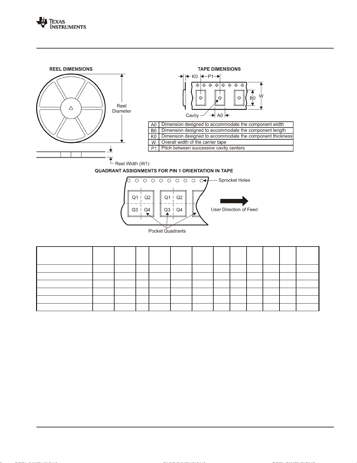
PACKAGE MATERIALS INFORMATION
www.ti.com 4-Sep-2010
TAPE AND REEL INFORMATION
*All dimensions are nominal
Device Package
Type
BQ24380DSGR WSON DSG 8 3000 179.0 8.4 2.2 2.2 1.2 4.0 8.0 Q2
BQ24380DSGT WSON DSG 8 250 179.0 8.4 2.2 2.2 1.2 4.0 8.0 Q2
BQ24381DSGR WSON DSG 8 3000 179.0 8.4 2.2 2.2 1.2 4.0 8.0 Q2
BQ24381DSGT WSON DSG 8 250 179.0 8.4 2.2 2.2 1.2 4.0 8.0 Q2
BQ24382DSGR WSON DSG 8 3000 179.0 8.4 2.2 2.2 1.2 4.0 8.0 Q2
BQ24382DSGT WSON DSG 8 250 179.0 8.4 2.2 2.2 1.2 4.0 8.0 Q2
Package
Drawing
Pins SPQ Reel
Diameter
(mm)
Reel
Width
W1 (mm)
A0
(mm)B0(mm)K0(mm)P1(mm)W(mm)
Pin1
Quadrant
Pack Materials-Page 1

PACKAGE MATERIALS INFORMATION
www.ti.com 4-Sep-2010
*All dimensions are nominal
Device Package Type Package Drawing Pins SPQ Length (mm) Width (mm) Height (mm)
BQ24380DSGR WSON DSG 8 3000 195.0 200.0 45.0
BQ24380DSGT WSON DSG 8 250 195.0 200.0 45.0
BQ24381DSGR WSON DSG 8 3000 195.0 200.0 45.0
BQ24381DSGT WSON DSG 8 250 195.0 200.0 45.0
BQ24382DSGR WSON DSG 8 3000 195.0 200.0 45.0
BQ24382DSGT WSON DSG 8 250 195.0 200.0 45.0
Pack Materials-Page 2


IMPORTANT NOTICE
Texas Instruments Incorporated and its subsidiaries (TI) reserve the right to make corrections, enhancements, improvements and other
changes to its semiconductor products and services per JESD46, latest issue, and to discontinue any product or service per JESD48, latest
issue. Buyers should obtain the latest relevant information before placing orders and should verify that such information is current and
complete. All semiconductor products (also referred to herein as “components”) are sold subject to TI’s terms and conditions of sale
supplied at the time of order acknowledgment.
TI warrants performance of its components to the specifications applicable at the time of sale, in accordance with the warranty in TI’s terms
and conditions of sale of semiconductor products. Testing and other quality control techniques are used to the extent TI deems necessary
to support this warranty. Except where mandated by applicable law, testing of all parameters of each component is not necessarily
performed.
TI assumes no liability for applications assistance or the design of Buyers’ products. Buyers are responsible for their products and
applications using TI components. To minimize the risks associated with Buyers’ products and applications, Buyers should provide
adequate design and operating safeguards.
TI does not warrant or represent that any license, either express or implied, is granted under any patent right, copyright, mask work right, or
other intellectual property right relating to any combination, machine, or process in which TI components or services are used. Information
published by TI regarding third-party products or services does not constitute a license to use such products or services or a warranty or
endorsement thereof. Use of such information may require a license from a third party under the patents or other intellectual property of the
third party, or a license from TI under the patents or other intellectual property of TI.
Reproduction of significant portions of TI information in TI data books or data sheets is permissible only if reproduction is without alteration
and is accompanied by all associated warranties, conditions, limitations, and notices. TI is not responsible or liable for such altered
documentation. Information of third parties may be subject to additional restrictions.
Resale of TI components or services with statements different from or beyond the parameters stated by TI for that component or service
voids all express and any implied warranties for the associated TI component or service and is an unfair and deceptive business practice.
TI is not responsible or liable for any such statements.
Buyer acknowledges and agrees that it is solely responsible for compliance with all legal, regulatory and safety-related requirements
concerning its products, and any use of TI components in its applications, notwithstanding any applications-related information or support
that may be provided by TI. Buyer represents and agrees that it has all the necessary expertise to create and implement safeguards which
anticipate dangerous consequences of failures, monitor failures and their consequences, lessen the likelihood of failures that might cause
harm and take appropriate remedial actions. Buyer will fully indemnify TI and its representatives against any damages arising out of the use
of any TI components in safety-critical applications.
In some cases, TI components may be promoted specifically to facilitate safety-related applications. With such components, TI’s goal is to
help enable customers to design and create their own end-product solutions that meet applicable functional safety standards and
requirements. Nonetheless, such components are subject to these terms.
No TI components are authorized for use in FDA Class III (or similar life-critical medical equipment) unless authorized officers of the parties
have executed a special agreement specifically governing such use.
Only those TI components which TI has specifically designated as military grade or “enhanced plastic” are designed and intended for use in
military/aerospace applications or environments. Buyer acknowledges and agrees that any military or aerospace use of TI components
which have not been so designated is solely at the Buyer's risk, and that Buyer is solely responsible for compliance with all legal and
regulatory requirements in connection with such use.
TI has specifically designated certain components as meeting ISO/TS16949 requirements, mainly for automotive use. In any case of use of
non-designated products, TI will not be responsible for any failure to meet ISO/TS16949.
Products Applications
Audio www.ti.com/audio Automotive and Transportation www.ti.com/automotive
Amplifiers amplifier.ti.com Communications and Telecom www.ti.com/communications
Data Converters dataconverter.ti.com Computers and Peripherals www.ti.com/computers
DLP® Products www.dlp.com Consumer Electronics www.ti.com/consumer-apps
DSP dsp.ti.com Energy and Lighting www.ti.com/energy
Clocks and Timers www.ti.com/clocks Industrial www.ti.com/industrial
Interface interface.ti.com Medical www.ti.com/medical
Logic logic.ti.com Security www.ti.com/security
Power Mgmt power.ti.com Space, Avionics and Defense www.ti.com/space-avionics-defense
Microcontrollers microcontroller.ti.com Video and Imaging www.ti.com/video
RFID www.ti-rfid.com
OMAP Applications Processors www.ti.com/omap TI E2E Community e2e.ti.com
Wireless Connectivity www.ti.com/wirelessconnectivity
Mailing Address: Texas Instruments, Post Office Box 655303, Dallas, Texas 75265
Copyright © 2013, Texas Instruments Incorporated

 Loading...