

Texas Instruments BQ24296, bq24297 Datasheet

User's Guide
SLUUAQ1–August 2013
bq24296/7 EVM (PWR021) User’s Guide
Contents
1 Introduction .................................................................................................................. 2
1.1 EVM Features ...................................................................................................... 2
1.2 I/O Descriptions .................................................................................................... 2
2 Test Summary ............................................................................................................... 4
2.1 Equipment ........................................................................................................... 4
2.2 Equipment Setup ................................................................................................... 5
2.3 Procedure ........................................................................................................... 6
3 PCB Layout Guideline .................................................................................................... 10
4 Board Layout, Schematic, and Bill of Materials ....................................................................... 11
4.1 Board Layout ...................................................................................................... 11
4.2 Schematic ......................................................................................................... 17
4.3 Bill of Materials .................................................................................................... 18
List of Figures
1 Connections of the HPA172 Kit........................................................................................... 5
2 Original Test Setup for PWR021 (bq2429xEVM) ...................................................................... 5
3 Main Window of the bq2429x Evaluation Software .................................................................... 6
4 CHG Mode Ripple and Duty Cycle: V
5 Boost Mode Ripple and Duty Cycle; V
6 bq2429xEVM Top Layer.................................................................................................. 11
7 bq2429xEVM Second Layer ............................................................................................. 12
8 bq2429xEVM Third Layer ................................................................................................ 13
9 bq2429xEVM Bottom Layer.............................................................................................. 14
10 bq2429xEVM Top Assembly............................................................................................. 15
11 bq2429xEVM Bottom Assembly......................................................................................... 16
12 bq24x9xEVM Schematic.................................................................................................. 17
= 5 V, V
BUS
= 3.7 V ...................................................................... 9
BAT
= 3.7 V.......................................................... 8
BAT
List of Tables
1 Device Data Sheets ........................................................................................................ 2
2 EVM Connections........................................................................................................... 2
3 Jumper Connections........................................................................................................ 3
4 Recommended Operating Conditions.................................................................................... 3
5 Device ID JEITA Settings.................................................................................................. 9
6 Bill of Materials............................................................................................................. 18
Windows is a trademark of Microsoft Corporation.
SLUUAQ1–August 2013 bq24296/7 EVM (PWR021) User’s Guide
Submit Documentation Feedback
Copyright © 2013, Texas Instruments Incorporated
1

Introduction
1 Introduction
1.1 EVM Features
For detailed features and operation, refer to Table 1 for a list of devices and their data sheets.
The bq24296 and bq24297 evaluation module (EVM) is a complete charger module for evaluating an I2Ccontrolled single NVDC-1 charge using the bq24296 and bq24297 devices.
This EVM doesn’t include the USB-to-GPIO interface board. To evaluate the EVM, a USB-to-GPIO
interface board must be ordered separately.
1.2 I/O Descriptions
Table 2 lists the jumper connections available on this EVM.
Jack Description
J1–PMID PMID pin connection/Power bank output
J1–VBUS Input: positive terminal
J1–GND Input: negative terminal (ground terminal)
J2-SYS Connected to system
J2-BAT+ Connected to battery pack
J2-GND Ground
J3 USB-to-GPIO connector (USB Interface Adapter Connector - HPA172)
J4–INT INT pin connection
J4– OTG OTG pin connection
J4-CE CE pin connection
J4-GND Ground
J5-TS2 External TS2 pin connection
J5-GND Ground
J6-TS1 External TS1 pin connection
J6-GND Ground
J7 Mini_USB Connector
www.ti.com
Table 1. Device Data Sheets
Device Document
bq24296/7 SLUSBP6
Table 2. EVM Connections
2
bq24296/7 EVM (PWR021) User’s Guide SLUUAQ1–August 2013
Copyright © 2013, Texas Instruments Incorporated
Submit Documentation Feedback
www.ti.com
Table 3 lists the controls and key parameter settings for this EVM.
Table 4 lists the recommended operating conditions for this EVM.
Introduction
Table 3. Jumper Connections
Jack Description Factory Setting
JP1 For bq24296/7 input current setting: bq24297: Not installed
PSEL LOW: Adaptor input bq24296:
PSEL HIGH: USB input Short PSEL to LOW
JP2 D-/PG pin selection bq24297: Short D-/PG to D-
bq24296:
Short D-/PG to PG
JP3 STAT, PG, /CE, INT, OTG pin internal pull-up source (VSYS) jumper Installed
JP4 USB current limit selection pin during buck mode and PSEL is high (JP1- Not installed
High)/Enable pin during boost mode.
In buck mode: OTG = High, IIN limit = 500 mA;
OTG = Low, IIN limit = 100 mA.
The boost mode is activated when the REG01[5:4] = 10 and OTG pin is
HIGH.
JP5 CE pin setting: pull low to enable the charge Not Installed
(GUI also can pull /CE low)
JP6 For bq24297 input current limit setting: bq24297: installed
bq24296: Not installed
JP7 TS1 resistor divider pull-up source (REGN) connection Installed
JP8 internal 10k to ground to TS1 Installed
JP9 internal 10k to ground to TS2 Installed
JP10 TS2 pin setting: bq24296/7: Short TS2 and TS2-I
Table 4. Recommended Operating Conditions
Symbol Description MIN TYP MAX Unit
Supply voltage, VINbq24296/7 Input voltage from AC adapter 3.9 5 6 VDC
Battery voltage, V
Supply current, I
Output current, I
Operating junction temperature 0 125 °C
range, T
BAT
AC
OUT
J
Voltage applied at V
Maximum input current from AC adapter 0 3 A
input
Output current 0 4 A
terminal 0 3.7 4.25 V
BAT
SLUUAQ1–August 2013 bq24296/7 EVM (PWR021) User’s Guide
Submit Documentation Feedback
Copyright © 2013, Texas Instruments Incorporated
3

Test Summary
2 Test Summary
Section 2.1 – Section 2.3 explains the equipment, the equipment setup, and the test procedures.
2.1 Equipment
2.1.1 Power Supplies
Power supply #1 (PS#1): a power supply capable of supplying 5 V at 1 A is required. While this part can
handle larger voltage and current, it is not necessary for this procedure.
2.1.2 Load #1 (4-Quadrant Supply, Constant Voltage < 4.5 V)
A 0–20 V/0–5 A, > 30-W system, DC electronic load and setting as constant voltage load mode.
Or:
Kepco load: BOP 20–5M, DC 0 to ±20 V, 0 to ±5 A (or higher)
Or:
Real single-cell battery
2.1.3 Load#2 – Use with Boost Mode
PMID to GND load, 10 Ω, 5 W or greater
www.ti.com
2.1.4 Meters
Six Fluke 75 multimeters, (equivalent or better)
Or:
Four equivalent voltage meters and two equivalent current meters.
The current meters must be capable of measuring 5 A+ current.
2.1.5 Computer
A computer with at least one USB port and a USB cable. The bq2429xEVM evaluation software must be
properly installed.
2.1.6 USB-to-GPIO Communication Kit (HPA172-USB Interface Adapter)
2.1.7 Software
Unzip the bq2429xEVM_GUI.zip and double-click on the SETUP.EXE file. Follow the installation steps.
The software supports the Windows™ XP and Windows 7 operating systems.
4
bq24296/7 EVM (PWR021) User’s Guide SLUUAQ1–August 2013
Copyright © 2013, Texas Instruments Incorporated
Submit Documentation Feedback
To Computer
USB Port
USB Interface
Adapter
I/O
USB
10-pin
Ribbon Cable
‘To EVM’
Texas Instruments
©
2006
www.ti.com
2.2 Equipment Setup
1. Set PS#1 for 5-V DC, 1-A current limit and then turn off the supply.
2. Connect the output of PS#1 in series with a current meter (multimeter) to J1 (V
3. Connect a voltage meter across J1 (V
4. Turn on the Load, set to constant voltage mode and output to 2.5 V. Turn off (disable) Load. Connect
Load in series with a current meter (multimeter), ground side, to J2 (BAT+ and GND) as shown in
Figure 2.
5. Connect a voltage meter across J2 (BAT+ and GND).
6. Connect the HPA172 USB interface adapter to the computer with a USB mini-cable and to J3 with the
10-pin ribbon cable. The connections are shown in Figure 1.
) and J1 (GND).
BUS
and GND).
BUS
Test Summary
Figure 1. Connections of the HPA172 Kit
7. Install shunts as shown in Table 3.
Figure 2. Original Test Setup for PWR021 (bq2429xEVM)
SLUUAQ1–August 2013 bq24296/7 EVM (PWR021) User’s Guide
Submit Documentation Feedback
Copyright © 2013, Texas Instruments Incorporated
5
Test Summary
8. Turn on the computer. Launch the bq2429x evaluation software. The main window of the bq2429x
software is shown in Figure 3.
www.ti.com
Figure 3. Main Window of the bq2429x Evaluation Software
2.3 Procedure
2.3.1 Current Settings
1. Make Sure EQUIPMENT SETUP steps are followed.
ILIM Setting: Set the potentiometer to its lowest value for max input current by connecting an ohmmeter between point TP9 and ground. Turn the screw on the potentiometer counterclockwise until the
resistance drops to its lowest point (this should be in the range of 125 Ω to 175 Ω, the value of R7)
2. Launch the Bq2429x EVM GUI software, if not already done
3. Turn on PS#1
Measure → V (J2(SYS), J2(GND)) = 4.10 ±300 mV
6
bq24296/7 EVM (PWR021) User’s Guide SLUUAQ1–August 2013
Copyright © 2013, Texas Instruments Incorporated
Submit Documentation Feedback
www.ti.com
2.3.2 Charge Voltage and Current Regulation of VINand Device ID Verification
Follow the steps and verify the outputs and IC for the EVM.
2.3.2.1 Software setup (all of Section 2.3.2.1 is done in the GUI):
1. Device address: bq24296/7
2. Click the Read button
3. Select Disabled for I2C Watchdog Timer Limit
4. Set Input Voltage Limit to 4.2 V
5. Set Input Current Limit to 500 mA
6. Set Charge Voltage Limit to 4.208 V
7. Set Fast Charge Current, ICHG to 512 mA
8. Set Pre-Charge Current to 256 mA
9. Deselect Enable Termination (see the following image)
Test Summary
10. Click the Read button twice
Observe → Everything normal at FAULT box
Observe → D1 (STAT) is on
Observe → D2 (/PG) is on for the bq24296EVM
2.3.2.2 Enable Load#1 from Section 2.2 step 4. Measure the voltage across J2 at two different points:
Measure → V(J2(SYS), J2(GND)) = 3.65 V ±300 mV
Measure → V(J2(BAT), J2(GND)) = 2.5 V ±200 mV
SLUUAQ1–August 2013 bq24296/7 EVM (PWR021) User’s Guide
Submit Documentation Feedback
Copyright © 2013, Texas Instruments Incorporated
7
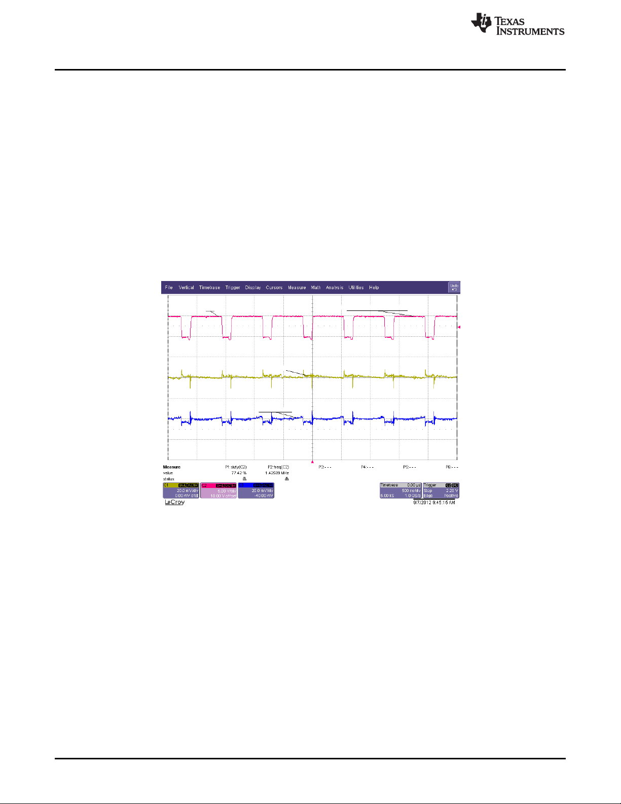
CHG Mode: VBUS = 5 V VBAT = 3.7 V
Vsw
Vsys_AC coupled
Vprnid_AC coupled
C2
C1
C3
Test Summary
www.ti.com
2.3.2.3 Increase the Constant Voltage Load to 3.7 V
DC
Measure → V(J2(SYS), J2(GND)) = 3.75 V ±200 mV
Measure → IBAT = 500 mA ±200 mA
Measure → V(J2(BAT), J2(GND)) = 3.7 V ±200 mV
2.3.2.4 In the software, set Fast Charge Current, ICHG to 1.012 A
Measure → Iin = 500 mA ±200 mA
2.3.2.5 Verify Scope Measurements (See Figure 4 – 500 ns/div)
C1 (AC coupled 20 mV/div): Vac_PMID (TP20 to GND) – Ripple excluding high frequency spikes < 10 mV
C2 (5 V/div): Vdc_SW (TP2) - Frequency between 1.25 MHz and 1.5 MHz, duty cycle between 73% and
81%
C3 (AC coupled 20 mV/div): Vac_VSYS (TP3 to GND) - excluding high frequency spikes < 15 mV
Figure 4. CHG Mode Ripple and Duty Cycle: V
8
bq24296/7 EVM (PWR021) User’s Guide SLUUAQ1–August 2013
Copyright © 2013, Texas Instruments Incorporated
BUS
= 5 V, V
= 3.7 V
BAT
Submit Documentation Feedback
 Loading...