1
mF
C
VREF
L
O
1.0 Hm
10nF
C
BOOT
+
PACK-
PACK+
1
mF
C
AUXPWR
SCL
SDA
CSOUT
CSIN
PGND
SW
I2CBUS
bq24155
10kW
VAUX
HOST
SCL
SDA
STAT
VREF
STAT
PMID
VBUS
C
IN
V
BUS
C
IN
1 Fm
4.7 Fm
BOOT
ISEL
U1
AUXPWR
ISEL
C
O
10
mF
R
SNS
0.1
mF
10kW
10kW
10kW
SGND
bq24155
www.ti.com
SLUS942 –FEBRUARY 2010
Fully Integrated Switch-Mode One-Cell Li-Ion Charger with Full USB Compliance
Check for Samples: bq24155
1
FEATURES
2
• Charge Faster than Linear Chargers
• High-Accuracy Voltage and Current Regulation
– Input Current Regulation Accuracy: ±5%
(100 mA and 500 mA)
– Charge Voltage Regulation Accuracy:
±0.5% (25°C), ±1% (0°C-125°C)
– Charge Current Regulation Accuracy: ±5%
• High-Efficiency Mini-USB/AC Battery Charger
for Single-Cell Li-Ion and Li-Polymer Battery
Packs
• 20-V Absolute Maximum Input Voltage Rating
• 6-V Maximum Operating Input Voltage
• Built-In Input Current Sensing and Limiting
• Integrated Power FETs for Up To 1.25-A
Charge Rate
• Programmable Charge Parameters through
I2C™ Compatible Interface (up to 3.4 Mbps):
– Input Current
– Fast-Charge/Termination Current
– Charge Voltage (3.5 V to 4.44 V)
– Safety Timer with Reset Control
– Termination Enable
• Synchronous Fixed-Frequency PWM
Controller Operating at 3 MHz with 0% to
99.5% Duty Cycle
• Automatic High Impedance Mode for Low
Power Consumption
• Robust Protection
– Reverse Leakage Protection Prevents
Battery Drainage
– Thermal Regulation and Protection
– Input/Output Overvoltage Protection
• Status Output for Charging and Faults
• USB Friendly Boot-Up Sequence
• Automatic Charging
• Power Up System without Battery
• 3.5 mm x 3.5 mm 14-Pin QFN Package
APPLICATIONS
• Mobile and Smart Phones
• MP3 Players
• Handheld Devices
DESCRIPTION
The bq24155 is a compact, flexible, high-efficiency,
USB-friendly switch-mode charge management
device for single-cell Li-ion and Li-polymer batteries
used in a wide range of portable applications. The
charge parameters can be programmed through an
I2C interface. The bq24155 integrates a synchronous
PWM controller, power FETs, input current sensing,
high-accuracy current and voltage regulation, and
charge termination, into a small WCSP package.
The bq24155 charges the battery in three phases:
conditioning, constant current and constant voltage.
The input current is automatically limited to the value
set by the host. Charge is terminated based on
user-selectable minimum current level. A safety timer
with reset control provides a safety backup for I2C
interface. During normal operation, bq24155
automatically restarts the charge cycle if the battery
voltage falls below an internal threshold and
automatically enters sleep mode or high impedance
mode when the input supply is removed. The charge
status is reported to the host using the I2C compatible
interface.
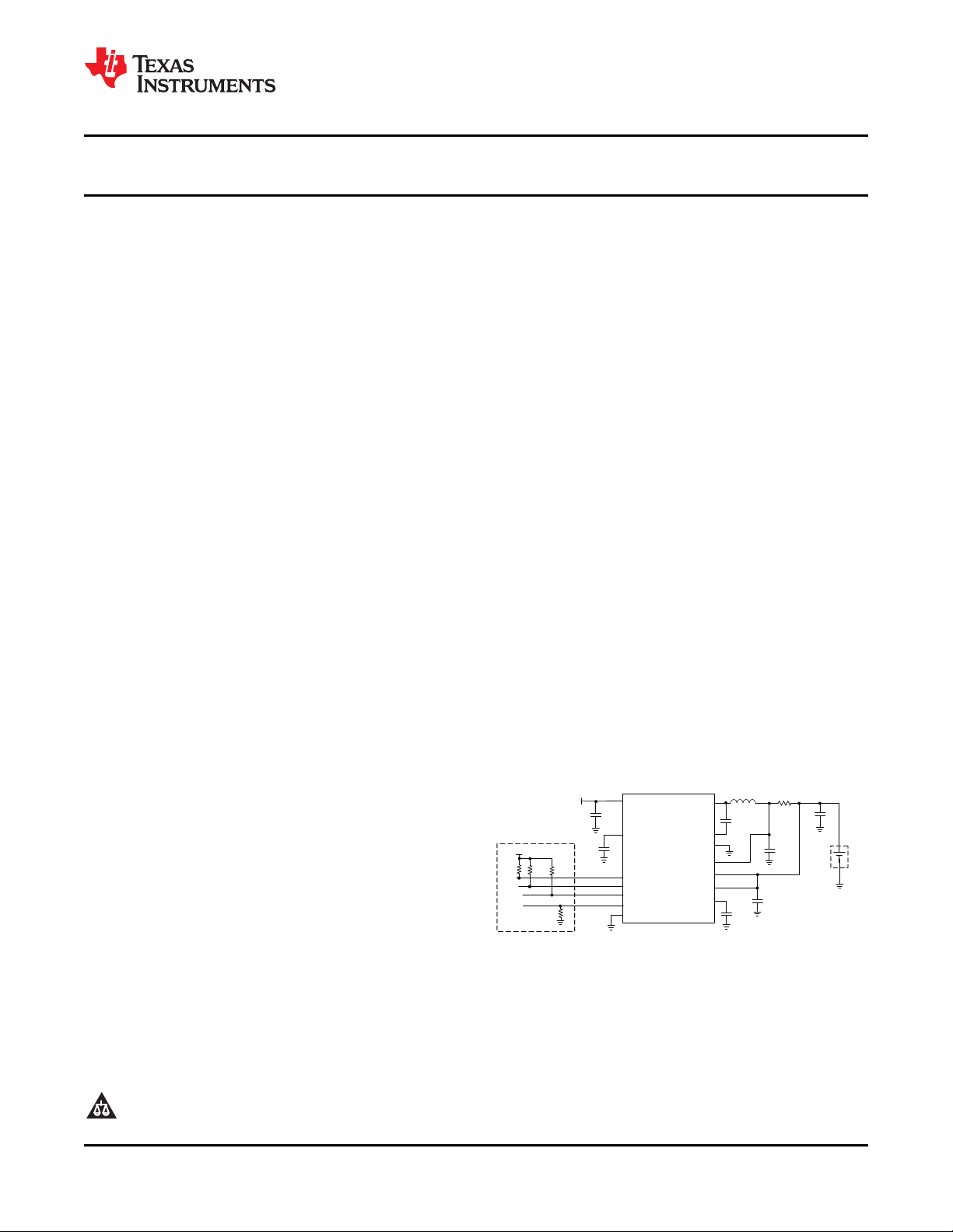
Typical Application Circuit
1
2I
PRODUCTION DATA information is current as of publication date.
Products conform to specifications per the terms of the Texas
Instruments standard warranty. Production processing does not
necessarily include testing of all parameters.
2
Please be aware that an important notice concerning availability, standard warranty, and use in critical applications of Texas
Instruments semiconductor products and disclaimers thereto appears at the end of this data sheet.
C is a trademark of Philips Electronics.
Copyright © 2010, Texas Instruments Incorporated
3
2
1 14
7 8
4
6
5
11
12
13
9
10
PMID
Thermal
Pad
SW
PGND
SGND
BOOT
VBUS
CSIN
AUXPWR VREF
SCL
SDA
STAT
ISEL
CSOUT
bq24155
SLUS942 –FEBRUARY 2010
www.ti.com
This integrated circuit can be damaged by ESD. Texas Instruments recommends that all integrated circuits be handled with
appropriate precautions. Failure to observe proper handling and installation procedures can cause damage.
ESD damage can range from subtle performance degradation to complete device failure. Precision integrated circuits may be more
susceptible to damage because very small parametric changes could cause the device not to meet its published specifications.
DESCRIPTION CONTINUED
During the charging process, the bq24155 monitors its junction temperature (TJ) and reduces the charge current
once TJincreases to approximately 125°C. The bq24155 is available in 14-pin QFN package.
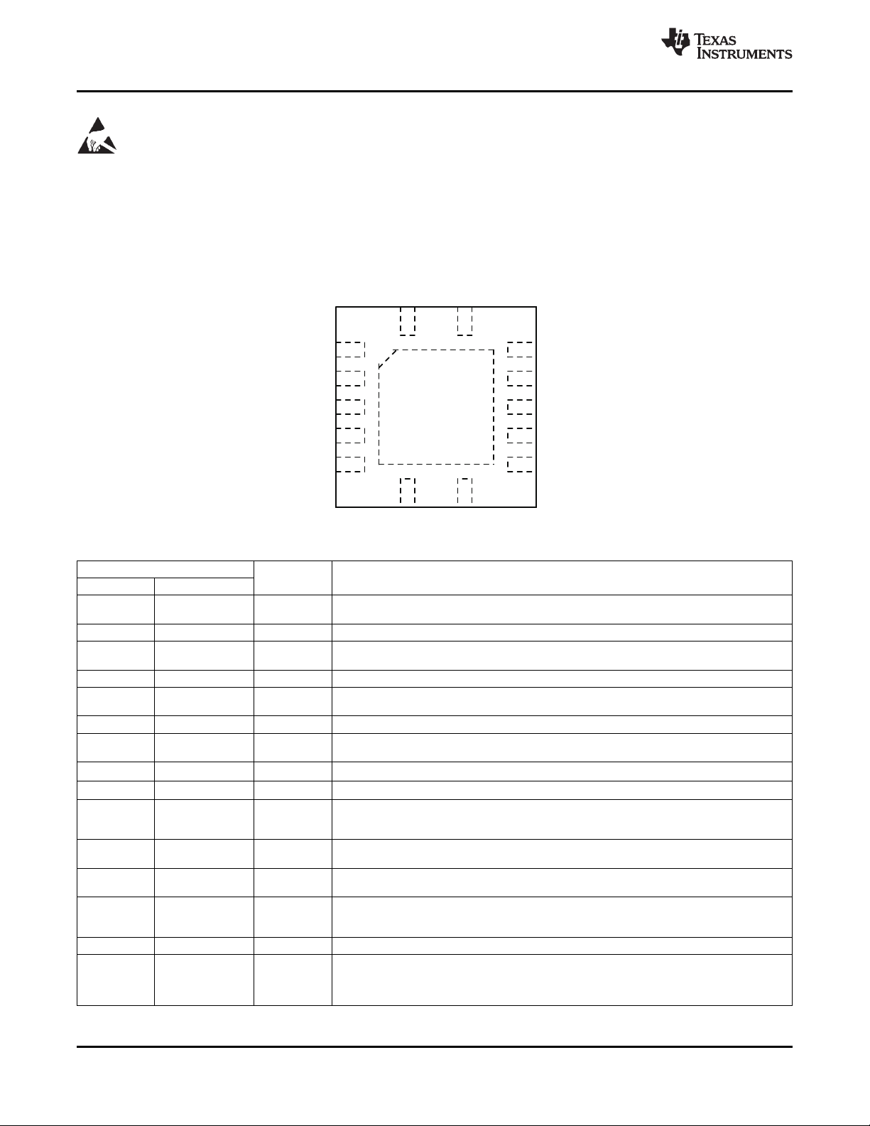
RGY PACKAGE
(Top View)
TERMINAL FUNCTIONS
TERMINAL
NAME NO.
CSOUT 6 I
VBUS 14 I Charger input voltage. Bypass it with a 1-mF ceramic capacitor from VBUS to PGND.
PMID 13 O
SW 12 O Internal switch to output inductor connection.
BOOT 1 O
PGND 11 Power ground
CSIN 9 I
SCL 2 I
SDA 3 I/O
STAT 4 O 128mS pulse is sent out. STAT pin can be disabled by the EN_STAT bit in control register. STAT can
VREF 8 O
AUXPWR 7 I
ISEL 5 I current limiting selection pin. When ISEL = High, Iin – limit = 500 mA and when ISEL = Low, Iin – limit
SGND 10 - Signal ground
Thermal pad pad -
2 Submit Documentation Feedback Copyright © 2010, Texas Instruments Incorporated
I/O DESCRIPTION
Battery voltage and current sense input. Bypass it with a ceramic capacitor (minimum 0.1 mF) to
PGND if there are long inductive leads to battery.
Connection point between reverse blocking FET and high-side switching FET. Bypass it with a
minimum of 3.3-mF capacitor from PMID to PGND.
Bootstrap capacitor connection for the high-side FET gate driver. Connect a 10-nF ceramic capacitor
(voltage rating above 10 V) from BOOT pin to SW pin.
Charge current-sense input. Battery current is sensed across an external sense resistor. A 0.1-mF
ceramic capacitor to PGND is required.
I2C interface clock. Open drain output, connect a 10-kΩ pullup resistor to 1.8V rail
I2C interface data. Open drain output, connect a 10-kΩ pullup resistor to 1.8V rail
Charge status pin. Pull low when charge in progress. Open drain for other conditions. During faults, a
be used to drive a LED or communicate with a host processor.
Internal bias regulator voltage. Connect a 1-mF ceramic capacitor from this output to PGND. External
load on VREF is not allowed.
Auxiliary power supply, connected to the battery pack to provide power in high-impedance mode.
Bypass it with a 1-mF ceramic capacitor from this pin to PGND.
Input current limiting selection pin. In 32 minutes mode, the ISEL pin is default to be used as the input
= 100 mA, see the Control Register for details.
There is an internal electrical connection between the exposed thermal pad and the PGND pin of the
device. The thermal pad must be connected to the same potential as the PGND pin on the printed
circuit board. Do not use the thermal pad as the primary ground input for the device. PGND/SGND
must be connected to ground at all times.
Product Folder Link(s): bq24155
bq24155
www.ti.com
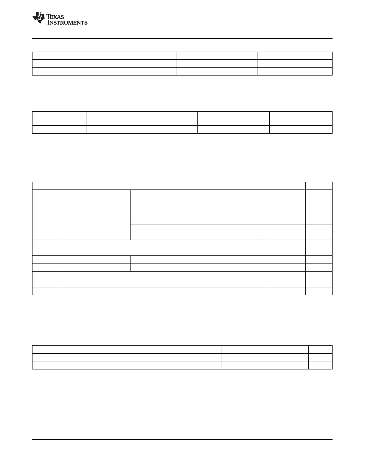
ORDERING INFORMATION
(1)
SLUS942 –FEBRUARY 2010
Part NO. MARKING MEDIUM QUANTITY
bq24155RGYR bq24155 Tape and Reel 3000
bq24155RGYT bq24155 Tape and Reel 250
(1) For the most current package and ordering information, see the Package Option Addendum at the end of this document, or see the TI
website at www.ti.com.
DISSIPATION RATINGS
PACKAGE R
QFN-14
(1)
(1)
qJA
55°C/W
R
qJC
(2)
15°C/W 1.82 W 0.018 W/°C
TA≤ 25°C DERATING FACTOR
POWER RATING TA> 25°C
(1) Maximum power dissipation is a function of TJ(max), RqJAand TA. The maximum allowable power dissipation at any allowable ambient
temperature is PD= [TJ(max)-TA] / RqJA.
(2) This data is based on using a JEDEC High-K 4-layer board and the exposed die pad is connected to a Cu pad on the board. The pad is
connected to the ground plane by a via matrix.
ABSOLUTE MAXIMUM RATINGS
(1) (2)
over operating free-air temperature range (unless otherwise noted)
VALUE UNIT
V
SS
V
I
Supply voltage range (with
respect to PGND)
Input voltage range (with
respect to and PGND)
VBUS –0.3 to 20
SCL, SDA, ISEL, CSIN, CSOUT, AUXPWR –0.3 to 7 V
PMID, STAT –0.3 to 20 V
V
O
Output voltage range (with
respect to and PGND)
VREF 6.5 V
SW, BOOT –0.7 to 20 V
Voltage difference between CSIN and CSOUT inputs (V
Voltage difference between BOOT and SW inputs (V
(BOOT)-V(SW)
(CSIN)-V(CSOUT)
) ±7 V
) –0.3 to 7 V
Output sink STAT 10 mA
I
O
T
A
T
J
T
stg
Output current (average) SW 1.25 A
Operating free-air temperature range –40 to 85 °C
Junction temperature –40 to 150 °C
Storage temperature –65 to 150 °C
(1) Stresses beyond those listed under absolute maximum ratings may cause permanent damage to the device. These are stress ratings
only, and functional operation of the device at these or any other conditions beyond those indicated under recommended operating
conditions is not implied. Exposure to absolute-maximum-rated conditions for extended periods may affect device reliability. All voltage
values are with respect to the network ground terminal unless otherwise noted.
(2) All voltages are with respect to PGND if not specified. Currents are positive into, negative out of the specified terminal.
(3) The bq24155 family can withstand up to 10.6 V continuously and 20 V for a minimum of 432 hours.
(3)
V
RECOMMENDED OPERATING CONDITIONS
MIN NOM MAX UNIT
V
BUS
T
J
Supply voltage, VBUS 4 6
Operating junction temperature range 0 +125 °C
(1) The inherent switching noise voltage spikes should not exceed the absolute maximum rating on either the BOOT or SW pins. A tight
layout minimizes switching noise.
Copyright © 2010, Texas Instruments Incorporated Submit Documentation Feedback 3
Product Folder Link(s): bq24155
(1)
V
bq24155
SLUS942 –FEBRUARY 2010
www.ti.com
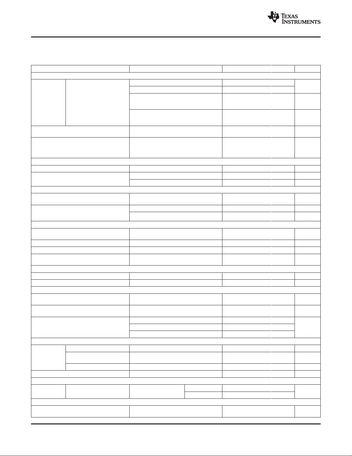
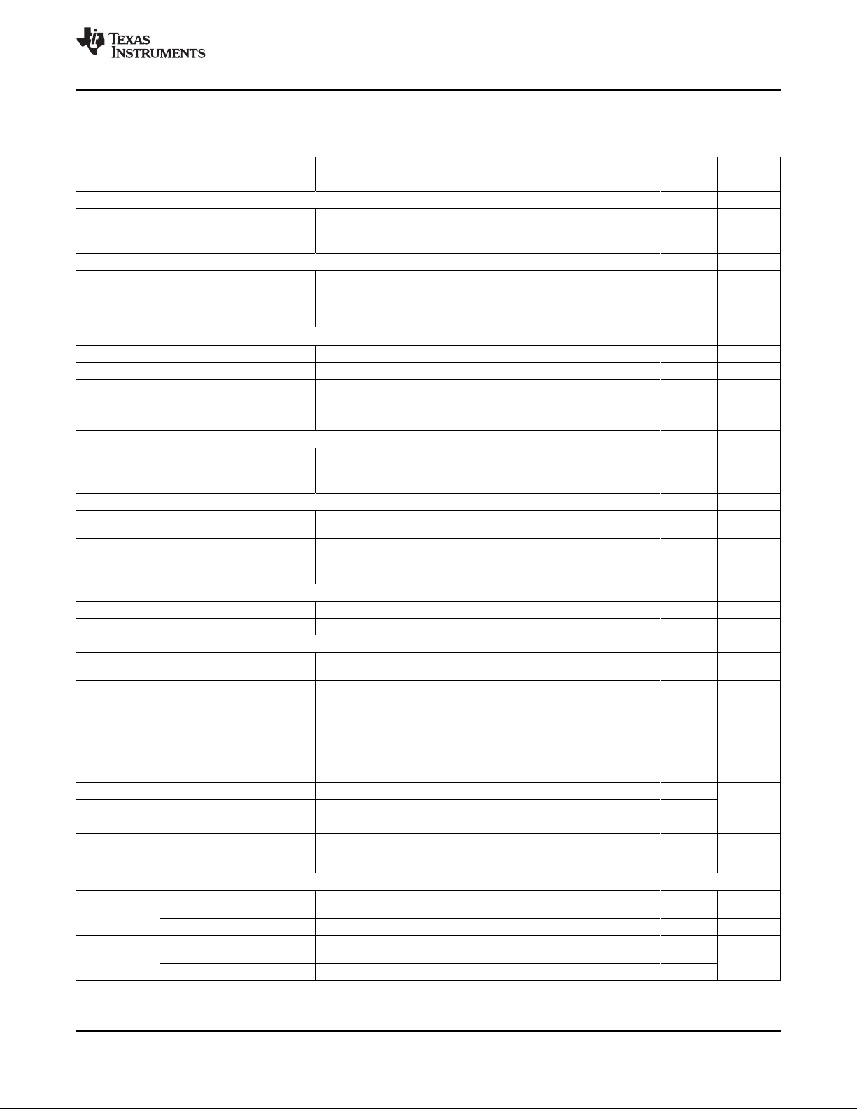
ELECTRICAL CHARACTERISTICS
Circuit of Figure 1, VBUS = 5 V, HZ_MODE = 0, OPA_MODE = 0 (charger mode operation), TJ= 0°C to 125°C, TJ= 25°C for
typical values (unless otherwise noted)
PARAMETER TEST CONDITIONS MIN TYP MAX UNIT
INPUT CURRENTS
VBUS > VBUS(min), PWM switching 10 mA
VBUS > VBUS(min), PWM NOT switching 5
0°C < TJ< 85°C, VBUS = 5 V, HZ_MODE = 1,
I
(VBUS)
VBUS supply current control
V
1.8 V
0°C < TJ< 85°C, VBUS = 5 V, HZ_MODE = 1,
V
= 0 V or 1.8 V
I
lkg
Leakage current from battery to 0°C < TJ< 85°C, V
VBUS pin impedance mode
Battery discharge current in High
Impedance mode, (CSIN, 20 mA
CSOUT, AUXPWR, SW pins)
0°C < TJ< 85°C, V
impedance mode,
VBUS = 0 V,
SCL, SDA, ISEL = 0 V or 1.8 V
VOLTAGE REGULATION
V
(OREG)
Output charge voltage Operating in voltage regulation, programmable 3.5 4.44 V
Voltage regulation accuracy
TA= 25°C –0.5% 0.5%
CURRENT REGULATION (FAST CHARGE)
I
O(CHARGE)
Output charge current V
programmable range R
Regulation accuracy for charge 20 mV ≤ V
current across R
V
(IREG)
= I
O(CHARGE)
(SNS)
× R
(SNS)
40 mV < V
WEAK BATTERY DETECTION
V
(LOWV)
Weak battery voltage threshold Programmable 3.4 3.7 V
programmable range
Weak battery voltage accuracy –5% 5%
Hysteresis for V
(LOWV)
Battery voltage falling 100 mV
Deglitch time for weak battery Rising voltage, 2 mV overdrive, t
threshold
ISEL PIN LOGIC LEVEL
V
IL
V
IH
Input low threshold level 0.4 V
Input high threshold level 1.3 V
CHARGE TERMINATION DETECTION
I
(TERM)
Termination charge current V
programmable range VBUS> V
Deglitch time for charge Both rising and falling, 2 mV overdrive, t
termination = 100 ns
Voltage regulation accuracy for
termination current across R
V
(IREG_TERM)
= I
O(TERM)
× R
(SNS)
(SNS)
3.4 mV ≤ V
6.8 mV ≤ V
13.6 mV ≤ V
INPUT POWER SOURCE DETECTION
Input voltage lower limit Input power source detection, Input voltage falling 3.6 3.8 4 V
VIN(min) Rising voltage, 2 mV overdrive, t
Deglitch time for VBUS rising ms
above VIN(min)
Hysteresis for VIN(min) Input voltage rising 100 200 mV
t
INT
Detection Interval Input power source detection 2 S
INPUT CURRENT LIMITING
I
IN
Input current limiting threshold USB charge mode
VREF BIAS REGULATOR
V
REF
Internal bias regulator voltage 2 6.5
VBUS >VIN(min) or V
I(VREF) = 1 mA, C(VREF) = 1 mF
> V
(AUXPWR)
(AUXPWR)
(LOWV)
(SNS)
(AUXPWR)
(LOWV)
< V
(LOWV)
≤ V
(AUXPWR)
= 68 mΩ Programmable
≤ 40 mV –5% 5%
(IREG)
(IREG)
> V
(OREG)
, R
(SLP)
(SNS)
(IREG_TERM)
(IREG_TERM)
(IREG_TERM)
, SCL, SDA, ISEL = 0 V or 20 mA
, 32 S mode, SCL, SDA, ISEL 35 mA
= 4.2 V, High
(AUXPWR)
(AUXPWR)
= 4.2 V, High
5 mA
–1% 1%
< V
(OREG)
, VBUS > V
, 550
(SLP)
1250 mA
–3% 3%
= 100 ns
RISE
– V
, mA
(RCH)
= 68 mΩ Programmable
, t
RISE
FALL
50 400
30 ms
30 ms
< 6.8 mV –25% 25%
< 13.6 mV –10% 10%
≤ 27.2 mV –5% 5%
= 100 ns 30
RISE
IIN= 100 mA 88 93 98 mA
IIN= 500 mA 450 475 500
> V
(AUXPWR)
min, V
(BAT)
4 Submit Documentation Feedback Copyright © 2010, Texas Instruments Incorporated
Product Folder Link(s): bq24155
bq24155
www.ti.com
SLUS942 –FEBRUARY 2010
ELECTRICAL CHARACTERISTICS (continued)
Circuit of Figure 1, VBUS = 5 V, HZ_MODE = 0, OPA_MODE = 0 (charger mode operation), TJ= 0°C to 125°C, TJ= 25°C for
typical values (unless otherwise noted)
PARAMETER TEST CONDITIONS MIN TYP MAX UNIT
V
output short current limit 30 mA
REF
BATTERY RECHARGE THRESHOLD
V
(RCH)
STAT OUTPUTS
V
OL(STAT)
I2C BUS LOGIC LEVELS AND TIMING CHARACTERISTICS
V
OL
V
IL
V
IH
I
(BIAS)
f
(SCL)
BATTERY DETECTION
I
(DETECT)
SLEEP COMPARATOR
V
(SLP)
V
(SLP_EXIT)
UNDERVOLTAGE LOCKOUT
UVLO IC active threshold voltage VBUS rising 3.05 3.3 3.55 V
UVLO
(HYS)
PWM
f
(OSC)
D
(MAX)
D
(MIN)
CHARGE MODE PROTECTION
V
(OVP-IN)
V
(OVP)
Recharge threshold voltage Below V
Deglitch time 130 ms
Low-level output saturation
voltage, STAT
High-level leakage current for
STAT
(OREG)
V
t
decreasing below threshold,
(AUXPWR)
= 100ns, 10 mV overdrive
FALL
IO= 10 mA, sink current 0.4 V
Voltage on STAT pin is 5 V 1 mA
100 120 150 mV
Output low threshold level IO= 10 mA, sink current 0.4 V
Input low threshold level 0.4 V
Input high threshold level 1.2 V
Input bias current V
= 1.8 V, SDA and SCL 1 mA
(pull-up)
SCL clock frequency 3.4 MHz
Battery detection current before Begins after termination detected,
charge done (sink current)
(1)
V
(AUXPWR)
≤ V
(OREG)
–0.45 mA
Battery detection time 262 ms
Sleep-mode entry threshold,
V
- V
BUS
AUXPWR
Sleep-mode exit hysteresis 2.3 V ≤ V
Deglitch time for VBUS rising
above V
(SLP)
+ V
(SLP_EXIT)
2.3 V ≤ V
(AUXPWR)
(AUXPWR)
≤ V
≤ V
(OREG)
(OREG)
, V
BUS
Rising voltage, 2-mV overdrive, t
falling 0 40 100 mV
40 100 160 mV
= 100ns 30 ms
RISE
IC active hysteresis VBUS falling from above UVLO 120 150 mV
Voltage from BOOT pin to SW
pin
Internal top reverse blocking FET I
on-resistance PMID
Internal top N-channel Switching
FET on-resistance
Internal bottom N-channel FET
on-resistance
During charge or boost operation 6.5 V
= 500 mA, Measured from VBUS to
IN(LIMIT)
Measured from PMID to SW, V
- VSW= 4 V 120 250 mΩ
BOOT
180 250
Measured from SW to PGND 110 200
Oscillator frequency 3 MHz
Frequency accuracy –10% 10%
Maximum duty cycle 99.5%
Minimum duty cycle 0
Synchronous mode to
non-synchronous mode transition Low side FET cycle by cycle current sensing 100 mA
current threshold
Input VBUS OVP threshold Threshold over VBUS to turn off converter during
voltage charge
V
(OVP_IN)
Output OVP threshold voltage 110 117 121
V
hysteresis Lower limit for V
(OVP)
(2)
hysteresis VBUS falling from above V
V
threshold over V
(CSOUT)
during charge
falling from above V
(CSOUT)
(OVP_IN)
to turn off charger
(OREG)
(OVP)
6.3 6.5 6.7 V
140 mV
%V
11
(OREG)
(1) Negative charge current means the charge current flows from the battery to charger (discharging battery).
(2) Bottom N-channel FET always turns on for Ⅹ60 ns and then turns off if current is too low.
Copyright © 2010, Texas Instruments Incorporated Submit Documentation Feedback 5
Product Folder Link(s): bq24155
C
VREF
10 nF
C
BOOT
+
PACK
-
PACK
+
C
AUXPWR
SCL
SDA
CSOUT
CSIN
PGND
SW
I
2
CBUS
VAUX
HOST
SCL
SDA
STAT
VREF
STAT
PMID
VBUS
C
IN
V
BUS
C
IN
BOOT
ISEL
U1
AUXPWR
ISEL
C
O
R
SNS
C
CSIN
V
BAT
1 Fm
4.7 Fm
10kW
10kW
10kW
10kW
10kW
L 1.0 HOm
68mW
10 Fm
0.1 Fm
1 Fm
1 Fm
bq24155
SGND
bq24155
SLUS942 –FEBRUARY 2010
www.ti.com
ELECTRICAL CHARACTERISTICS (continued)
Circuit of Figure 1, VBUS = 5 V, HZ_MODE = 0, OPA_MODE = 0 (charger mode operation), TJ= 0°C to 125°C, TJ= 25°C for
typical values (unless otherwise noted)
PARAMETER TEST CONDITIONS MIN TYP MAX UNIT
I
(LIMIT)
V
(SHORT)
I
(SHORT)
PROTECTION
T
(SHTDWN)
T
(CF)
T
(32S)
(3) Verified by design
Cycle-by-cycle current limit for
charge
Short-circuit voltage threshold V
V
hysteresis V
(SHORT)
Short-circuit current V
Thermal trip 165
Thermal hysteresis 10 °C
Thermal regulation threshold
Time constant for the 32 second
timer
Charge mode operation 1.5 2.3 3 A
falling 1.9 2 2.1 V
(AUXPWR)
rising from below V
(AUXPWR)
≤ V
(AUXPWR)
(3)
Charge current begins to reduce 120
32 Second mode 12 32 s
(SHORT)
(SHORT)
5 10 15 mA
100 mV
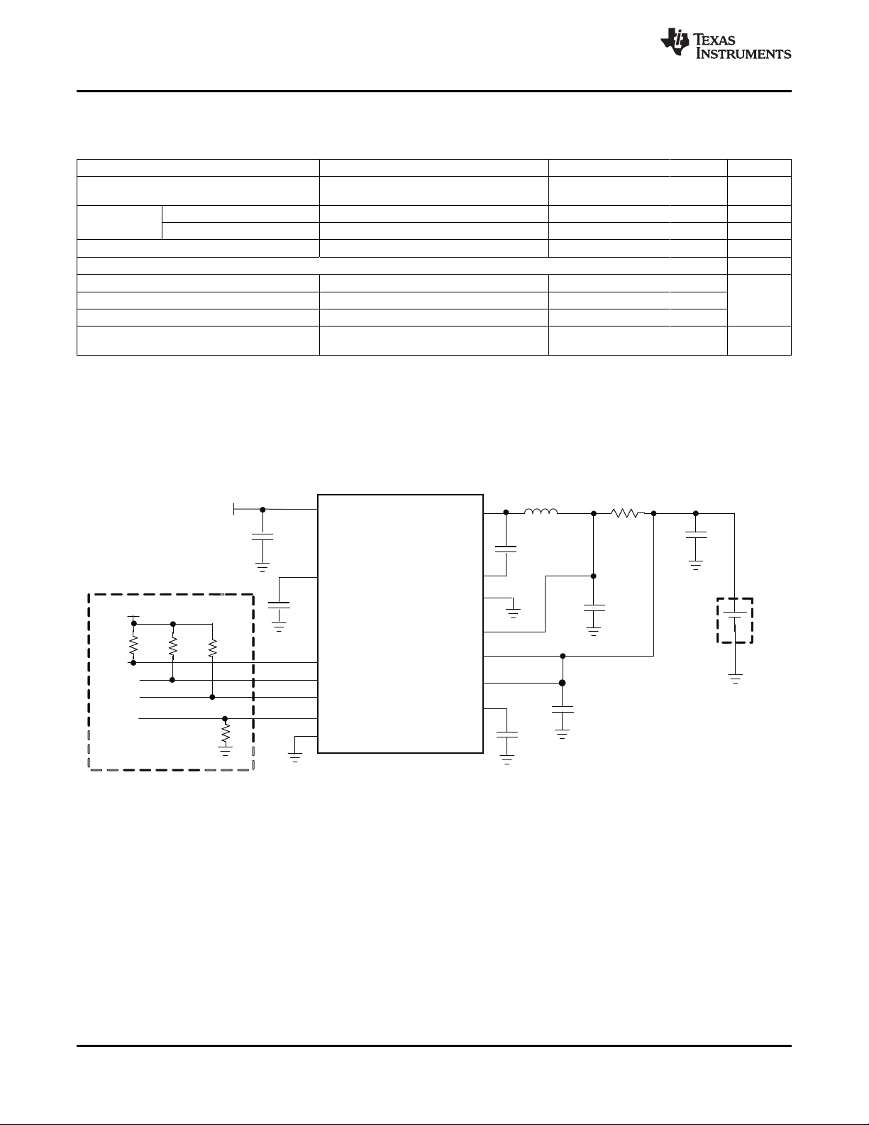
TYPICAL APPLICATION CIRCUITS
VBUS = 5 V, I
seconds.
(CHARGE)
= 1250 mA, VBAT = 3.5 V to 4.44 V (adjustable), Safety Timer = 32 minutes or 32
Figure 1. I2C Controlled 1-Cell Charger Application Circuit
VBUS = 5 V, I
(IN_LIMIT)
6 Submit Documentation Feedback Copyright © 2010, Texas Instruments Incorporated
= 500 mA, V
= 3.5 V to 4.44 V (adjustable), Safety Timer = 32 minutes or 32 seconds.
OUT
Product Folder Link(s): bq24155
+
PACK
-
V
SYS
Host
-
Controlled
Switch
PACK
+
SCL
SDA
CSOUT
CSIN
PGND
SW
I
2
CBUS
VAUX
HOST
SCL
SDA
STAT
VREF
STAT
PMID
VBUS
C
IN
V
BUS
C
IN
1 Fm
BOOT
ISEL
U1
AUXPWR
C
VREF
C
O
C
BOOT
R
SNS
C
CSIN
1 Fm
C
AUXPWR
C
CSOUT
ISEL
10nF
68mW
V
OUT
4.7 Fm
10kW
10kW
10kW
10kW
10kW
LO1.0 Hm
0.1 Fm
10 Fm
0.1 Fm
1 Fm
bq24155
Host
Charge
Controller
Q
SGND
VBUS
2V/div
I
0.5 A/div
BAT
500 S/divm
Vbus=0–5V,Vbat=3.5VChargemode
VSW
5V/div
VBAT
2V/div
VSW
5V/div
I
0.5 A/div
BAT
1S/div
Vbus=5V,Iin_limit=500mA,
32SMode
VSW
2V/div
IL
0.5 A/div
Vbus=5V Vbat=2.6V,Voreg=4.2V,Ichg=1250mA,
100nS/div
VBUS
2V/div
VSW
5V/div
I
0.1 A/div
BUS
2mS/div
Vbus=5V@10mA,Iin_limit=100mA,
Vbat=3.2V,Ichg=550mA
bq24155
www.ti.com
TYPICAL APPLICATION CIRCUITS (continued)
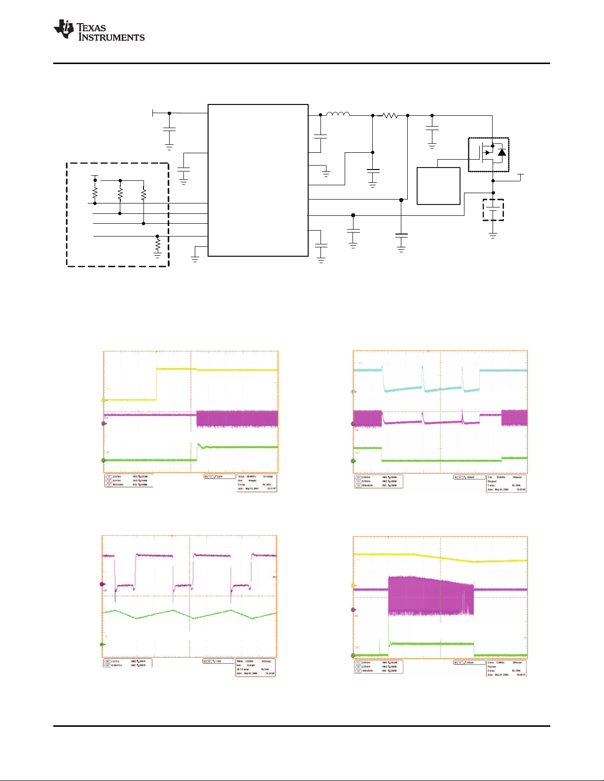
Figure 2. I2C Controlled 1-Cell Pre-Regulator Application
TYPICAL CHARACTERISTICS
Using circuit shown in Figure 1, TA= 25°C, unless otherwise specified.
ADAPTER INSERTION BATTERY INSERTION/REMOVAL
SLUS942 –FEBRUARY 2010
Figure 3. Figure 4.
PWM CHARGING WAVEFORMS POOR SOURCE DETECTION
Copyright © 2010, Texas Instruments Incorporated Submit Documentation Feedback 7
Figure 5. Figure 6.
Product Folder Link(s): bq24155
VSW
2V/div
I
0.5 A/div
L
2 S/divm
Vbus=5V,Vbat=3.6VChargemode
operation
V
5V/div
BUS
V
1V/div
BAT
ISEL
5V/div
I
50mA/div
BAT
20mS/div
V =0-5V,
NoBattery,
C =100 F,
R =5k
IN
OUT
LOAD
m
W
ISEL
5V/div
I
0.2 A/div
BUS
0.5S/div
Vbus=5V,Iin_limit=100/500mA,
(ISEL Control,32MinuteMode),
Iin_limit=100mA (I CControl,32SecondMode)
2
32Minute
Mode
32Second
Mode
80
82
84
86
88
90
92
0 100 200 300 400 500 600 700 800 900 1000 1100 12001300
ChargeCurrent-mA
Efficiency-%
Vbat=4V
Vbat=3V
Vbat=3.6V
V =5V
BUS
bq24155
SLUS942 –FEBRUARY 2010
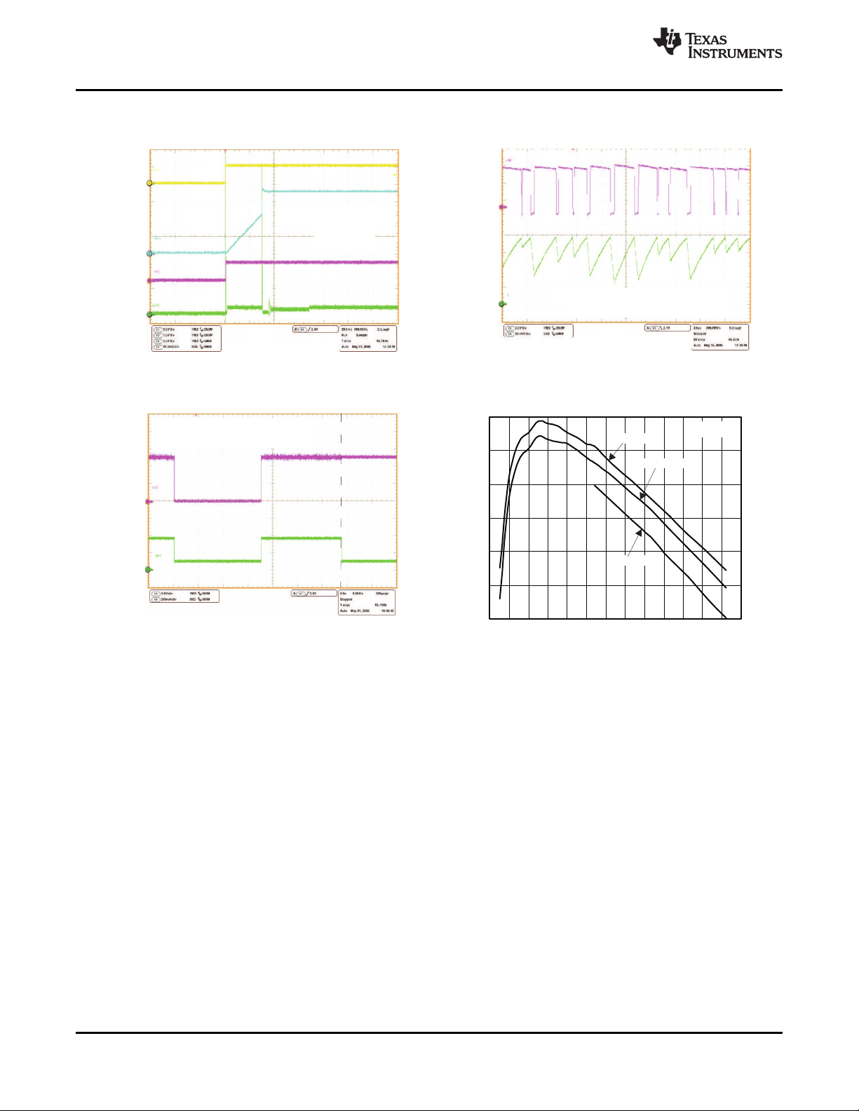
BATTERY DETECTION AT POWER UP CYCLE BY CYCLE CURRENT LIMIT IN CHARGE MODE
INPUT CURRENT CONTROL CHARGER EFFICIENCY
www.ti.com
TYPICAL CHARACTERISTICS (continued)
Figure 7. Figure 8.
Figure 9. Figure 10.
8 Submit Documentation Feedback Copyright © 2010, Texas Instruments Incorporated
Product Folder Link(s): bq24155
SW
bq24155
CHARGECONTROL,
TIMERandDISPLAY
LOGIC
*
Sleep
CSOUT
CSIN
STAT
PGND
SW
PGND
SCL
NMOS
NMOS
NMOS
PMID
SDA
(I2CControl)
Decoder
DAC
Q2
Q3
VREF
PMID
Q1
BOOT
REFERNCES
& BIAS
PMID
VBUS
SW
V
PMID
PGND
VBUS
V
PMID
ISEL
AUXPWR
I
SHORT
VREF
LINEAR _CHG
+
-
-
+
-
-
+
-
+
-
T
J
T
CF
I
OCHARGE
V
OREG
VREF
Charge
Pump
VREF1
I
IN_
LIMIT
OSC
+
-
V
OVP
_IN
V
BUS
V
BUS
+
-
V
UVLO
V
BUS
+
V
IN(
MIN)
V
BUS
+
-
T
J
T
SHTDWN
CBC
Current
Limiting
PWM
Controller
I
LIMIT
+
-
V
BAT
V
BUS
VBAT
VOUT
VCSIN
*
BatteryOVP
+
-
V
OUT
V
OVP
VBUSUVLO
PoorInput
VBUSOVP
Thermal
Shutdown
*
Recharge
+
-
V
OUT
V
OREG-VRCH
*
SignalDeglitched
+
-
-
V
OUT
V
CSIN
I
TERM
*
PWM_CHG
*
PWMCharge
Mode
+
-
V
BAT
V
SHORT
Termination
VREF1
bq24155
www.ti.com
SLUS942 –FEBRUARY 2010
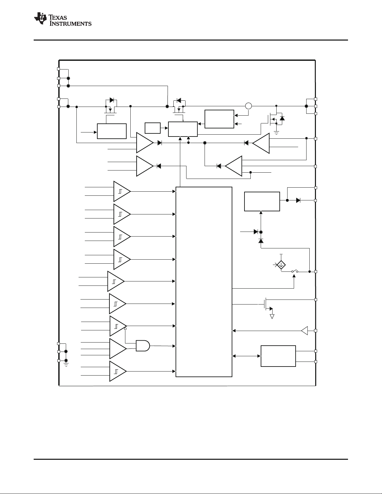
FUNCTIONAL BLOCK DIAGRAM (Charge Mode)
Copyright © 2010, Texas Instruments Incorporated Submit Documentation Feedback 9
Figure 11. Function Block Diagram of bq24155 in Charge Mode
Product Folder Link(s): bq24155
V
AUXPWR<VSHORT
?
Yes
No
32-Minute
TimerExpired?
No
EnableI
SHORT
IndicateCharge-In-
Progress
Regulate
InputCurrent, Charge
CurrentorVoltage
HighImpedanceModeorHost
ControlledOperationMode
TerminationEnabled
I
TERM
detected
andV
AUXPWR>VOREG-VRCH
?
Yes
V
AUXPWR
< V
OREG
-
V
RCH
?
V
AUXPWR<VSHORT
?
No
No
Yes
Yes
Yes
/CE=HIGH
TurnOffCharge
IndicateFault
IndicateShort
Circuitcondition
32-Minute
Timer Expired?
No
Yes
Yes
IndicateDONE
ChargeComplete
V
BUS<VIN(MIN)
?
Yes
No
IndicatePower
notGood
DisableCharge
WaitMode
Delay T
INT
V
BUS<VIN(MIN)
?
No
Yes
V
AUXPWR
< V
OREG
-
V
RCH
?
EnableI
DETECT
for
t
DETECT
TurnOffCharge
No
No
ResetCharge
Parameters
BatteryRemoved
WaitMode
Delay T
INT
Yes
V
AUXPWR<VLOWV
and bq24155?
PowerUp
V
BUS>VUVLO
No
Yes
Any ChargeState/CE=HIGH
ChargeConfigure
Mode
DisableCharge
/CE=LOW
32-Minute Timer
Active?
No
Yes
HighImpedance
Mode
ChargeComplete
ResetandStart
32-MinuteTimer
POR
LoadI2CRegisters
withDefaultValue
bq24155
SLUS942 –FEBRUARY 2010
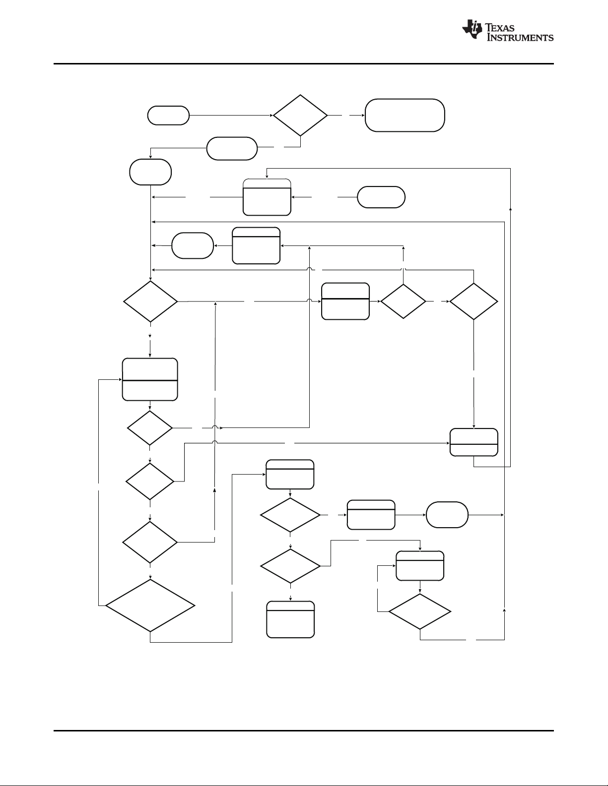
OPERATIONAL FLOW CHART
www.ti.com
Figure 12. Operational Flow Chart of bq24155 in Charge Mode
10 Submit Documentation Feedback Copyright © 2010, Texas Instruments Incorporated
Product Folder Link(s): bq24155

bq24155
www.ti.com
SLUS942 –FEBRUARY 2010
DETAILED FUNCTIONAL DESCRIPTION
For a current limited power source, such as a USB host or hub, a high efficiency converter is critical to fully use
the input power capacity for quickly charging the battery. Due to the high efficiency for a wide range of input
voltages and battery voltages, the switch mode charger is a good choice for high speed charging with less power
loss and better thermal management than a linear charger.
The bq24155 is a highly integrated synchronous switch-mode charger, featuring integrated FETs and small
external components, targeted at extremely space-limited portable applications powered by 1-cell Li-Ion or
Li-polymer battery pack.
The bq24155 has two operation modes: charge mode and high impedance mode. In charge mode, the bq24155
supports a precision Li-ion or Li-polymer charging system for single-cell applications. In high impedance mode,
the bq24155 stops charging and operates in a mode with low current from VBUS or battery, to effectively reduce
the power consumption when the portable device in standby mode. Through the proper control, bq24155
achieves the smooth transition among the different operation modes.
CHARGE MODE OPERATION
Charge Profile
In charge mode, bq24155 has four control loops to regulate input current, charge current, charge voltage and
device junction temperature, as shown in Figure 11. During the charging process, all four loops are enabled and
the one that is dominant takes control. The bq24155 supports a precision Li-ion or Li-polymer charging system
for single-cell applications. Figure 13(a) indicates a typical charge profile without input current regulation loop. It
is the traditional CC/CV charge curve, while Figure 13(b) shows a typical charge profile when input current
limiting loop is dominant during the constant current mode. In this case, the charge current is higher than the
input current so the charge process is faster than the linear chargers. For bq24155, the input current limits, the
charge current, termination current, and charge voltage are all programmable using I2C interface.
Copyright © 2010, Texas Instruments Incorporated Submit Documentation Feedback 11
Product Folder Link(s): bq24155
 Loading...