

1 Fm
1 Fm
1kW
1.5kW
1.5kW
2kW
Disconnect after Detection
+
Battery Pack
VBUS
GND
D+
D-
USB Port
DC+
GND
Adaptor
VDD
D-
D+
GND
TTDM
Host
System Load
OR
ISET/100/500mA
1
2
3
4
5
10
9
8
7
6
IN
ISET
VSS
PRETERM
PG
NC
ISET2
CHG
TS
OUT
bq2409x
+
www.ti.com
bq24090, bq24091
bq24092, bq24093
SLUS968B –JANUARY 2010–REVISED JUNE 2010
1A, Single-Input, Single Cell Li-Ion Battery Charger
Check for Samples: bq24090, bq24091, bq24092, bq24093
1
FEATURES
• CHARGING
– 1% Charge Voltage Accuracy
– 10% Charge Current Accuracy
– Pin Selectable USB 100mA and 500mA
Maximum Input Current Limit
– Programmable Termination and Precharge
Threshold
• PROTECTION
– 6.6V Over-Voltage Protection
– Input Voltage Dynamic Power Management
– 125°C Thermal Regulation; 150°C Thermal
Shutdown Protection
– OUT Short-Circuit Protection and ISET
Short Detection
– Operation Over JEITA Range via Battery
NTC – ½ Fast-Charge-Current at Cold,
4.06V at Hot, bq24092/3
– Fixed 10 Hour Safety Timer
• SYSTEM
– Automatic Termination and Timer Disable
Mode (TTDM) for Absent Battery Pack With
Thermistor
– Status Indication – Charging/Done
– Available in Small 10-Pin MSOP Package
APPLICATIONS
• Smart Phones
• PDAs
• MP3 Players
• Low-Power Handheld Devices
DESCRIPTION
The bq2409x series of devices are highly integrated
Li-ion linear chargers devices targeted at
space-limited portable applications. The devices
operate from either a USB port or AC adapter. The
high input voltage range with input overvoltage
protection supports low-cost unregulated adapters.
The bq2409x has a single power output that charges
the battery. A system load can be placed in parallel
with the battery as long as the average system load
does not keep the battery from charging fully during
the 10 hour safety timer.
The battery is charged in three phases: conditioning,
constant current and constant voltage. In all charge
phases, an internal control loop monitors the IC
junction temperature and reduces the charge current
if an internal temperature threshold is exceeded.
1
Please be aware that an important notice concerning availability, standard warranty, and use in critical applications of Texas
Instruments semiconductor products and disclaimers thereto appears at the end of this data sheet.
PRODUCTION DATA information is current as of publication date.
Products conform to specifications per the terms of the Texas
Instruments standard warranty. Production processing does not
necessarily include testing of all parameters.
Copyright © 2010, Texas Instruments Incorporated
bq24090, bq24091
bq24092, bq24093
SLUS968B –JANUARY 2010–REVISED JUNE 2010
These devices have limited built-in ESD protection. The leads should be shorted together or the device placed in conductive foam
during storage or handling to prevent electrostatic damage to the MOS gates.
DESCRIPTION CONTINUED
The charger power stage and charge current sense functions are fully integrated. The charger function has high
accuracy current and voltage regulation loops, charge status display, and charge termination. The pre-charge
current and termination current threshold are programmed via an external resistor. The fast charge current value
is also programmable via an external resistor.
ORDERING INFORMATION
PART # V
bq24090 4.20 V 6.6 V No 10kΩ NTC Yes 10 PIN 5x3mm
bq24091 4.20 V 6.6 V No 100kΩ NTC Yes 10 PIN 5x3mm
bq24092 4.20 V 6.6 V Yes 10kΩ NTC Yes 10 PIN 5x3mm
bq24093 4.20 V 6.6 V Yes 100kΩ NTC Yes 10 PIN 5x3mm
O(REG)
V
OVP
JEITA TS/CE PG PACKAGE Marking
2
2
2
2
www.ti.com
bq24090
bq24091
bq24092
bq24093
ABSOLUTE MAXIMUM RATINGS
(1)
over operating free-air temperature range (unless otherwise noted)
VALUE UNIT
IN (with respect to VSS) –0.3 to 7 V
Input Voltage
Input Current IN 1.25 A
Output Current (Continuous) OUT 1.25 A
Output Sink Current CHG 15 mA
T
T
(1) Stresses beyond those listed under absolute maximum ratings may cause permanent damage to the device. These are stress ratings
Junction temperature –40 to 150 °C
J
Storage temperature –65 to 150 °C
STG
only, and functional operation of the device at these or any other conditions beyond those indicated under recommended operating
conditions is not implied. Exposure to absolute-maximum-rated conditions for extended periods may affect device reliability. All voltage
values are with respect to the network ground terminal unless otherwise noted.
PACKAGE DISSIPATION RATINGS
PACKAGE R
5x3mm MSOP 52°C/W 48°C/W 1.92 W 19.2 mW/°C
(1) For the most current package and ordering information, see the Package Option Addendum at the end of this document, or see the TI
Web site at www.ti.com.
(2) This data is based on using the JEDEC High-K board and the exposed die pad is connected to a copper pad on the board. This is
connected to the ground plane by a 2×3 via matrix
OUT (with respect to VSS) –0.3 to 7 V
PRE-TERM, ISET, ISET2, TS, CHG, PG, ASI, ASO (with respect to
VSS)
(1) (2)
qJA
R
qJC
TA≤ 25°C DERATING FACTOR
POWER RATING TA> 25°C
–0.3 to 7 V
2 Submit Documentation Feedback Copyright © 2010, Texas Instruments Incorporated
Product Folder Link(s): bq24090 bq24091 bq24092 bq24093
www.ti.com
bq24090, bq24091
bq24092, bq24093
SLUS968B –JANUARY 2010–REVISED JUNE 2010
RECOMMENDED OPERATING CONDITIONS
(1)
MIN MAX UNIT
V
IN
I
IN
I
OUT
T
J
R
PRE-TERM
R
ISET
R
TS
IN voltage range 3.5 7 V
IN operating voltage range, Restricted by V
DPM
and V
OVP
4.45 6.45 V
Input current, IN pin 1.0 A
Current, OUT pin 1.0 A
Junction temperature 0 125 °C
Programs precharge and termination current thresholds 1 10 kΩ
Fast-charge current programming resistor 0.675 49.9 kΩ
10k NTC thermistor range without entering BAT_EN or TTDM 1.66 258 kΩ
(1) Operation with VINless than 4.5V or in drop-out may result in reduced performance.
ELECTRICAL CHARACTERISTICS
Over junction temperature range 0°C ≤ TJ≤ 125°C and recommended supply voltage (unless otherwise noted)
PARAMETER TEST CONDITIONS MIN TYP MAX UNIT
INPUT
UVLO Undervoltage lock-out Exit VIN: 0V → 4V Update based on sim/char 3.15 3.3 3.45 V
V
HYS_UVLO
V
IN-DT
V
HYS-INDT
t
DGL(PG_PWR)
t
DGL(PG_NO-
PWR)
V
OVP
t
DGL(OVP-SET)
V
HYS-OVP
t
DGL(OVP-REC)
V
IN-DPM
I
IN-USB-CL
Hysteresis on V
Input power good detection threshold
is V
+ V
OUT
IN-DT
Hysteresis on V
Deglitch time on exiting sleep. 45 ms
Deglitch time on V
down. Same as entering sleep. PG = OC, V
Input over-voltage protection threshold VIN: 5V → 7V 6.5 6.65 6.8 V
Input over-voltage blanking time VIN: 5V → 7V 113 ms
Hysteresis on OVP VIN: 7V → 5V 95 mV
Deglitch time exiting OVP 30 ms
USB/Adaptor low input voltage
protection. Restricts lout at V
USB input I-Limit 100mA ISET2 = Float; R
USB input I-Limit 500mA ISET2 = High; R
ISET SHORT CIRCUIT TEST
R
ISET_SHORT
t
DGL_SHORT
I
OUT_CL
Highest Resistor value considered a Riset: 600Ω → 250Ω, I
fault (short). Monitored for Iout>90mA Reset.
Deglitch time transition from ISET
short to Iout disable
Maximum OUT current limit Regulation
(Clamp)
BATTERY SHORT PROTECTION
V
OUT(SC)
V
OUT(SC-HYS)
I
OUT(SC)
OUT pin short-circuit detection
threshold/ precharge threshold
OUT pin Short hysteresis 77 mV
Source current to OUT pin during
short-circuit detection
UVLO_RISE
IN-DT
falling 175 227 280 mV
falling V
power Time measured from VIN: 5V → 3.2V 1ms fall-time to
HYS-INDT
IN-DPM
VIN: 4V→0V,
V
UVLO_FALL
(Input power good if VIN> V
V
OUT
OUT
= V
UVLO_RISE–VHYS-UVLO
+ V
= 3.6V, VIN: 3.5V → 4V
OUT
IN-DT
);
30 80 145 mV
= 3.6V, VIN: 4V → 3.5V 31 mV
Time measured from VIN: 0V → 5V 1ms rise-time to
PG = low, V
OUT
OUT
= 3.6V
= 3.6V
29 ms
Time measured from VIN: 7V → 5V 1ms fall-time to
PG = LO
Feature active in USB mode; Limit Input Source
Current to 50mA; V
OUT
= 3.5V; R
ISET
= 825Ω
Feature active in Adaptor mode; Limit Input Source
Current to 50mA; V
= 3.5V; R
OUT
= 825Ω 85 92 100
ISET
= 825Ω 430 462 500
ISET
latches off. Cycle power to
OUT
ISET
= 825Ω
4.34 4.4 4.46
4.24 4.3 4.36
280 500 Ω
Clear fault by cycling IN or TS/BAT_EN 1 ms
VIN= 5V, V
600Ω → 250Ω, Iout latches off after t
V
:3V → 0.5V, no deglitch 0.75 0.8 0.85 V
OUT
Recovery ≥ V
Deglitch
OUT
OUT(SC)
= 3.6V, V
+ V
= Low, R
ISET2
OUT(SC-HYS)
:
ISET
DGL-SHORT
; Rising, no
1.05 1.4 A
10 15 20 mA
V
mA
Copyright © 2010, Texas Instruments Incorporated Submit Documentation Feedback 3
Product Folder Link(s): bq24090 bq24091 bq24092 bq24093
bq24090, bq24091
bq24092, bq24093
SLUS968B –JANUARY 2010–REVISED JUNE 2010
ELECTRICAL CHARACTERISTICS (continued)
Over junction temperature range 0°C ≤ TJ≤ 125°C and recommended supply voltage (unless otherwise noted)
PARAMETER TEST CONDITIONS MIN TYP MAX UNIT
QUIESCENT CURRENT
I
OUT(PDWN)
I
OUT(DONE)
I
IN(STDBY)
I
CC
BATTERY CHARGER FAST-CHARGE
V
OUT(REG)
V
O_HT(REG)
I
OUT(RANGE)
V
DO(IN-OUT)
I
OUT
K
ISET
PRECHARGE – SET BY PRETERM PIN
V
LOWV
t
DGL1(LOWV)
t
DGL2(LOWV)
I
PRE-TERM
%
PRECHG
K
PRE-CHG
TERMINATION – SET BY PRE-TERM PIN
%
TERM
K
TERM
I
PRE-TERM
%TERM Termination current formula R
t
DGL(TERM)
I
Term-Start
t
Term-Start
Battery current into OUT pin VIN= 0V 1
OUT pin current, charging terminated VIN= 6V, V
OUT
> V
OUT(REG)
Standby current into IN pin TS = LO, VIN≤ 6V 125 mA
Active supply current, IN pin 0.8 1.0 mA
Battery regulation voltage VIN= 5.5V, I
Battery hot regulation Voltage,
bq24092/3
Programmed Output “fast charge”
current range
Drop-Out, VIN – VOUT 325 520 mV
Output “fast charge” formula V
Fast charge current factor R
Pre-charge to fast-charge transition
threshold
Deglitch time on pre-charge to
fast-charge transition
Deglitch time on fast-charge to
pre-charge transition
TS = open, VIN= 6V, TTDM – no load on OUT pin,
V
> V
OUT
VIN= 5.5V, I
V
OUT(REG)
R
= 675 to 10.8kΩ
ISET
Adjust VIN down until I
R
= 675 , ISET2=Lo (adaptor mode); TJ≤ 100°C
ISET
OUT(REG)
R
= K
ISET
= K
ISET
R
= K
ISET
OUT(REG)
OUT
OUT
> V
OUT
> V
OUT
ISET/IOUT
ISET/IOUT
ISET/IOUT
, IC enabled
= 25mA, (V
= 25mA, V
> V
LOWV
OUT
> V
LOWV
; 50 < I
; 25 < I
; 10 < I
≤ VTS≤ V
TS-45°C
TS-60°C
≤ VTS≤ V
TS-0°C
TS-45°C
; VIN= 5V, ISET2=Lo,
= 0.5A, V
OUT
= 4.15V,
; VIN= 5V, ISET2 = Lo K
< 800 mA 510 540 565
OUT
< 50 mA 480 527 580 AΩ
OUT
< 25 mA 350 520 680
OUT
) 4.16 4.2 4.23 V
4.02 4.06 4.1 V
10 1000 mA
ISET/RISET
2.4 2.5 2.6 V
70 ms
32 ms
Refer to the Termination Section
V
< V
; R
OUT
Pre-charge current, default setting 18 20 22
Pre-charge current formula R
% Pre-charge Factor
Termination Threshold Current, default V
setting R
Termination Current Threshold
Formula
% Term Factor Ω/%
LOWV
R
PRE-TERM
PRE-TERM
V
< V
OUT
LOWV
R
= 1080Ω , R
ISET
where %I
FAST-CHG
V
< V
OUT
LOWV
R
= 1080Ω, R
ISET
where %I
FAST-CHG
> V
OUT
RCH
PRE-TERM
R
PRE-TERM
V
> V
OUT
RCH
R
= 750Ω K
ISET
is 10 to 50%
V
> V
OUT
RCH
= 750Ω K
TERM
= High Z
= K
= High Z
= K
= 1080Ω; %I
ISET
(Ω/%) × %
PRE-CHG
, VIN= 5V, R
, VIN= 5V, R
; R
ISET
TERM
, VIN= 5V, R
TERM
, VIN= 5V, R
× %Iset, where %Iset is 5 to 10%
PRE-TERM
= K
PRE-TERM
is 20 to 100%
PRE-TERM
is 10% to 20%
PRE-CHG
PRE-TERM
= K
PRE-CHG
= 1k; %I
(Ω/%) × %TERM (%) R
PRE-TERM
× %I
FAST-CHG
PRE-TERM
(%) R
PRE-CHG
= 2k to 10kΩ;
× %I
FAST-CHG
= 1k to 2kΩ;
× %I
FAST-CHG
= 2k to 10kΩ ;
, where %I
FAST-CHG
= 1k to 2kΩ ; R
PRE-TERM/KPRE-CHG%
, 90 100 110 Ω/%
, 84 100 117 Ω/%
9 10 11
/ K
PRE-TERM
TERM
182 200 216
ISET
174 199 224
Current for programming the term. and
pre-chg with resistor. I
initial PRE-TERM current.
Term-Start
is the R
PRE-TERM
= 2k, V
= 4.15V 71 75 81 mA
OUT
/ K
TERM
TERM
Deglitch time, termination detected 29 ms
Elevated PRE-TERM current for,
t
, during start of charge to 80 85 92 mA
Term-Start
prevent recharge of full battery,
Elevated termination threshold initially
active for t
Term-Start
1.25 min
www.ti.com
mA
6
A
OUT-
CC
OUT-
CC
%
4 Submit Documentation Feedback Copyright © 2010, Texas Instruments Incorporated
Product Folder Link(s): bq24090 bq24091 bq24092 bq24093
bq24090, bq24091
bq24092, bq24093
www.ti.com
ELECTRICAL CHARACTERISTICS (continued)
Over junction temperature range 0°C ≤ TJ≤ 125°C and recommended supply voltage (unless otherwise noted)
PARAMETER TEST CONDITIONS MIN TYP MAX UNIT
RECHARGE OR REFRESH
Recharge detection threshold – V
V
RCH
Normal Temp -0.120 0.070
Recharge detection threshold – Hot V
Temp -0.130 0.080
t
DGL1(RCH)
t
DGL2(RCH)
Deglitch time, recharge threshold VIN= 5V, VTS= 0.5V, V
detected t
Deglitch time, recharge threshold VIN= 5V, VTS= 0.5V, V
detected in OUT-Detect Mode is time to ISET ramp
BATTERY DETECT ROUTINE
V
REG-BD
I
BD-SINK
t
DGL(HI/LOW
REG)
V
BD-HI
V
BD-LO
VOUT Reduced regulation during V
battery detect -0.450 350
Sink current during V
Regulation time at V
REG-BD
REG
or V
REG-BD
High battery detection threshold VIN= 5V, VTS= 0.5V, Battery Absent V
Low battery detection threshold VIN= 5V, VTS= 0.5V, Battery Absent V
BATTERY CHARGING TIMERS AND FAULT TIMERS
t
PRECHG
t
MAXCH
Pre-charge safety timer value 1700 1940 2250 s
Charge safety timer value 34000 38800 45000 s
BATTERY-PACK NTC MONITOR (Note 1); TS pin: 10k and 100k NTC
I
NTC-10k
I
NTC-100k
I
NTC-DIS-10k
I
NTC-DIS-100k
NTC bias current, bq24090/2 VTS= 0.3V 48 50 52 mA
NTC bias current, bq24091/3 VTS= 0.3V 4.8 5.0 5.2 mA
10k NTC bias current when Charging
is disabled, bq24090/2
10k NTC bias current when Charging
is disabled, bq24091/3
INTC is reduced prior to entering
I
NTC-FLDBK-10k
TTDM to keep cold thermistor from VTS: Set to 1.525V 4 5 6.5 mA
entering TTDM, bq24090/2
INTC is reduced prior to entering
I
NTC-FLDBK-100k
V
TTDM(TS)
V
HYS-TTDM(TS)
V
CLAMP(TS)
t
DGL(TTDM)
V
TS_I-FLDBK
C
TS
V
TS-0°C
V
HYS-0°C
V
TS-10°C
V
HYS-10°C
V
TS-45°C
V
HYS-45°C
TTDM to keep cold thermistor from VTS: Set to 1.525V 1.1 1.5 1.9 mA
entering TTDM, bq24091/3
Termination and timer disable mode
Threshold – Enter
Hysteresis exiting TTDM VTS: 1.7V → 0.5V; Timer Enabled 100 mV
TS maximum voltage clamp VTS= Open (Float) 1800 1950 2000 mV
Deglitch exit TTDM between states 57 ms
Deglitch enter TTDM between states 8 ms
TS voltage where INTC is reduce to
keep thermistor from entering TTDM
Optional Capacitance – ESD 0.22 mF
Low temperature CHG Pending 1205 1230 1255 mV
Hysteresis at 0°C 86 mV
Low temperature, half charge, Normal charging to low temp charging;
bq24092/3 VTS: 0.5V → 1V
Hysteresis at 10°C, bq24092/3 35 mV
High temperature at 4.1V 263 278 293 mV
Hysteresis at 45°C 10.7 mV
VIN= 5V, VTS= 0.5V, V
VIN= 5V, VTS= 0.2V, V
is time to ISET ramp
DGL(RCH)
: 4.25V → V
OUT
: 4.15V → V
OUT
: 4.25V → 3.5V in 1ms;
OUT
= 3.5V inserted; t
OUT
RCH
RCH
VIN= 5V, VTS= 0.5V, Battery Absent 7 10 mA
Restarts when entering Pre-charge; Always enabled
when in pre-charge.
Clears fault or resets at UVLO, TS/BAT_EN disable,
OUT Short, exiting LOWV and Refresh
VTS= 0V 27 30 34 mA
VTS= 0V 4.4 5.0 5.8 mA
VTS: 0.5V → 1.7V; Timer Held in Reset 1550 1600 1650 mV
INTC adjustment (90 to 10%; 45 to 6.6uS) takes
place near this spec threshold. VTS: 1.425V → 1475 mV
1.525V
Low Temp Charging to Pending;
VTS: 1.0V → 1.5V
Charge pending to low temp charging;
VTS: 1.5V → 1V
Low temp charging to normal CHG;
VTS: 1.0V → 0.5V
Normal charging to high temp CHG;
VTS: 0.5V → 0.2V
High temp charging to normal CHG;
VTS: 0.2V → 0.5V
SLUS968B –JANUARY 2010–REVISED JUNE 2010
O(REG)
V
-0.095 V
O(REG)
O(REG)
V
-0.105 V
O(REG)
29 ms
DGL(RCH)
O(REG)
V
3.6 ms
-0.400 V
O(REG)
25 ms
V
O(REG)
-0.150 0.050
V
REG-BD
+0.50 +0.15
-0.100 V
O(REG)
+0.1 V
REG-BD
765 790 815 mV
V
O(REG)
V
O(REG)
V
O(REG)
V
O(REG)
V
REG-BD
-
-
-
-
Copyright © 2010, Texas Instruments Incorporated Submit Documentation Feedback 5
Product Folder Link(s): bq24090 bq24091 bq24092 bq24093
bq24090, bq24091
bq24092, bq24093
SLUS968B –JANUARY 2010–REVISED JUNE 2010
ELECTRICAL CHARACTERISTICS (continued)
Over junction temperature range 0°C ≤ TJ≤ 125°C and recommended supply voltage (unless otherwise noted)
PARAMETER TEST CONDITIONS MIN TYP MAX UNIT
V
TS-60°C
V
HYS-60°C
t
DGL(TS_10C)
t
DGL(TS)
V
TS-EN-10k
V
TS-DIS_HYS-10k
V
TS-EN-100k
V
TS-DIS_HYS-
100k
High temperature Disable, bq24092/3 170 178 186 mV
Hysteresis at 60°C, bq24092/3 11.5 mV
Deglitch for TS thresholds: 10C,
bq24092/3
Deglitch for TS thresholds: 0/45/60C. Battery charging 30 ms
Charge Enable Threshold, (10k NTC) VTS: 0V → 0.175V; 80 88 96 mV
HYS below V
NTC)
TS-EN-10k
Charge Enable Threshold, bq24090/2 VTS: 0V → 0.175V; 140 150 160 mV
HYS below V
bq24091/3
TS-EN-100k
THERMAL REGULATION
T
J(REG)
T
J(OFF)
T
J(OFF-HYS)
Temperature regulation limit 125 °C
Thermal shutdown temperature 155 °C
Thermal shutdown hysteresis 20 °C
LOGIC LEVELS ON ISET2
V
IL
V
IH
I
IL
I
IH
V
FLT
Logic LOW input voltage Sink 8 mA 0.4 V
Logic HIGH input voltage Source 8 mA 1.4 V
Sink current required for LO V
Source current required for HI V
ISET2 Float Voltage 575 900 1225 mV
LOGIC LEVELS ON CHG AND PG
V
I
LEAK
OL
Output LOW voltage I
Leakage current into IC V
to Disable, (10k
to Disable,
High temp charge to pending;
VTS: 0.2V → 0.1V
Charge pending to high temp CHG;
VTS: 0.1V → 0.2V
Normal to Cold Operation; VTS: 0.6V → 1V 50
Cold to Normal Operation; VTS: 1V → 0.6V 12
VTS: 0.125V → 0V; 12 mV
VTS: 0.125V → 0V; 50 mV
= 0.4V 2 9 mA
ISET2
= 1.4V 1.1 8 mA
ISET2
= 5 mA 0.4 V
SINK
= 5V, VPG= 5V 1 mA
CHG
www.ti.com
ms
6 Submit Documentation Feedback Copyright © 2010, Texas Instruments Incorporated
Product Folder Link(s): bq24090 bq24091 bq24092 bq24093
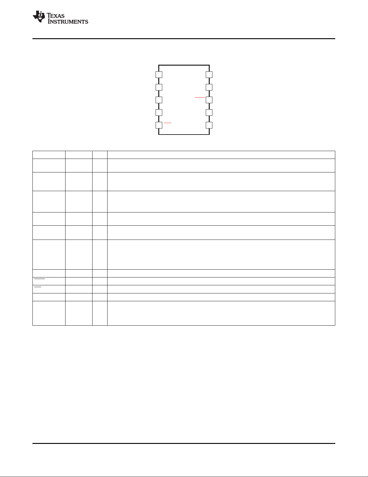
1
2
3
4
5
10
9
8
7
6
IN
ISET
VSS
PRETERM
PG
NC
ISET2
CHG
TS
OUT
bq2409x
bq24090, bq24091
bq24092, bq24093
www.ti.com
PIN CONFIGURATION
PIN FUNCTIONS
NAME PIN I/O DESCRIPTION
IN 1 I
OUT 10 O battery to charge within the 10 hour safety timer window. Expected range of bypass capacitors 1mF to
PRE-TERM 4 I
ISET 2 I
ISET2 7 I
TS 9 I Mode and disable TS monitoring, Timers and Termination. Pulling pin Low disables the IC. If NTC
VSS 3 – Ground terminal
CHG 8 O Low (FET on) indicates charging and Open Drain (FET off) indicates no Charging or Charge complete.
PG 5 O Low (FET on) indicates the input voltage is above UVLO and the OUT (battery) voltage.
NC 6 NA Do not make a connection to this pin (for internal use) – Do not route through this pin
Thermal PAD Pad device. The thermal pad must be connected to the same potential as the VSS pin on the printed circuit
and Package 5x3mm
2
Input power, connected to external DC supply (AC adapter or USB port). Expected range of bypass
capacitors 1mF to 10mF, connect from IN to VSS.
Battery Connection. System Load may be connected. Average load should not be excessive, allowing
10mF.
Programs the Current Termination Threshold (5 to 50% of Iout which is set by ISET) and Sets the
Pre-Charge Current to twice the Termination Current Level.
Expected range of programming resistor is 1k to 10kΩ (2k: Ipgm/10 for term; Ipgm/5 for precharge)
Programs the Fast-charge current setting. External resistor from ISET to VSS defines fast charge current
value. Range is 10.8k (50mA) to 675 Ω (800mA).
Programming the Input/Output Current Limit for the USB or Adaptor source:
High = 500mAmax, Low = ISET, FLOAT = 100mAmax.
Temperature sense pin connected to bq24090/2 -10k at 25°C NTC thermistor & bq24091/3 -100k at
25°C NTC thermistor, in the battery pack. Floating TS Pin or pulling High puts part in TTDM “Charger”
sensing is not needed, connect this pin to VSS through an external 10 kΩ/100kΩ resistor. A 250kΩ from
TS to ground will prevent IC entering TTDM mode when battery with thermistor is removed.
There is an internal electrical connection between the exposed thermal pad and the VSS pin of the
–
board. Do not use the thermal pad as the primary ground input for the device. VSS pin must be
connected to ground at all times
SLUS968B –JANUARY 2010–REVISED JUNE 2010
Copyright © 2010, Texas Instruments Incorporated Submit Documentation Feedback 7
Product Folder Link(s): bq24090 bq24091 bq24092 bq24093
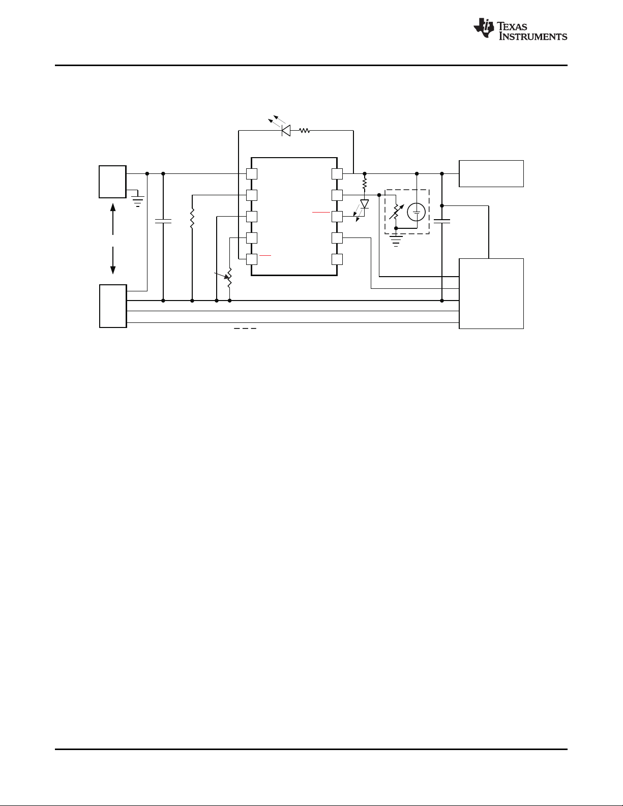
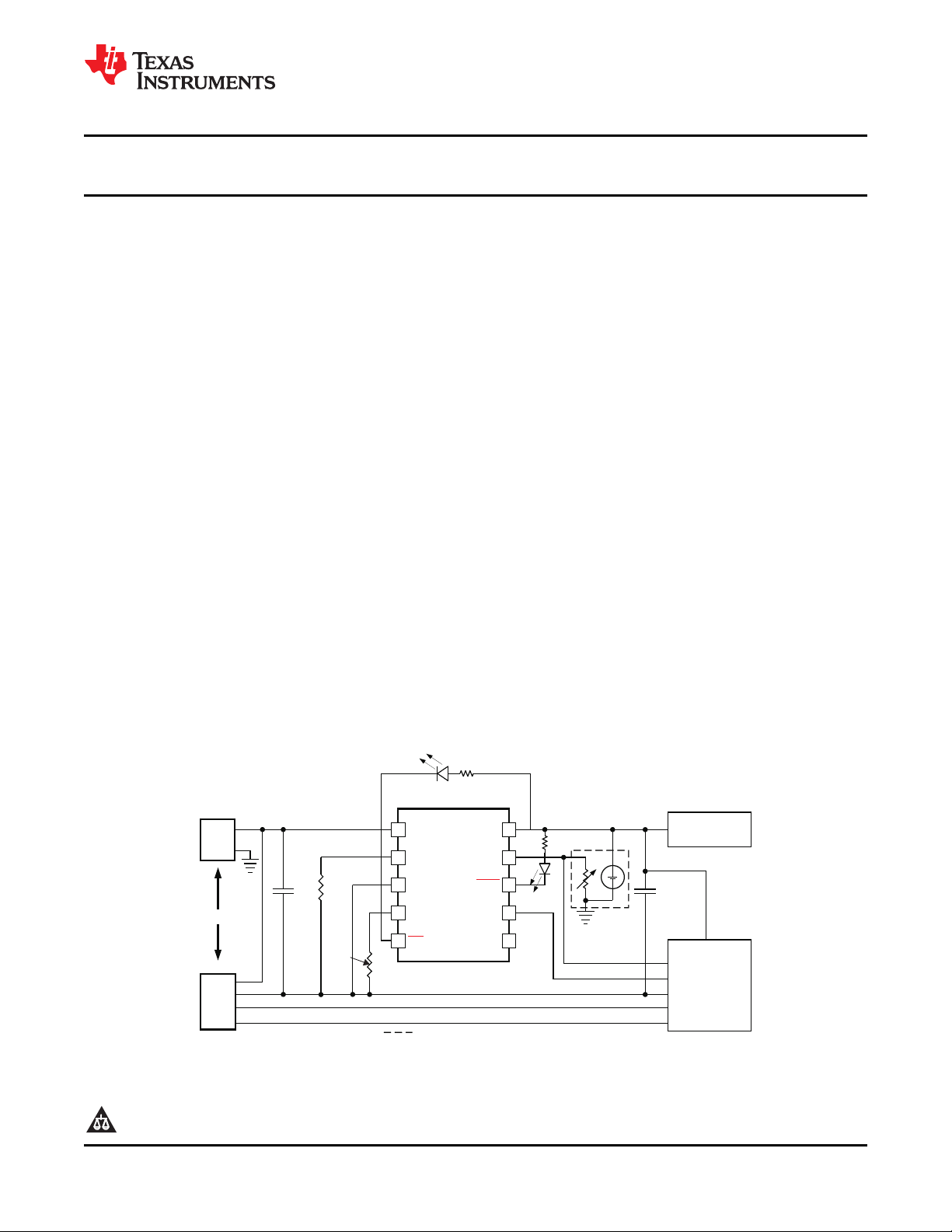
BatteryPack
VBUS
GND
D+
D-
USBPort
DC+
GND
Adaptor
VDD
D-
D+
GND
Host
SystemLoad
OR
ISET/100/500 mA
1
2
3
4
5
10
9
8
7
6
IN
ISET
VSS
PRETERM
PG
NC
ISET2
CHG
TS
OUT
bq2409x
1 Fm
1 Fm
1kW
1.5kW
1.5kW
2kW
DisconnectafterDetection
+
TTDM
+
bq24090, bq24091
bq24092, bq24093
SLUS968B –JANUARY 2010–REVISED JUNE 2010
Typical Application Circuit: bq2409x
I
OUT_FAST_CHG
= 540mA; I
OUT_PRE_CHG
= 108mA; I
OUT_TERM
www.ti.com
= 54mA
8 Submit Documentation Feedback Copyright © 2010, Texas Instruments Incorporated
Product Folder Link(s): bq24090 bq24091 bq24092 bq24093
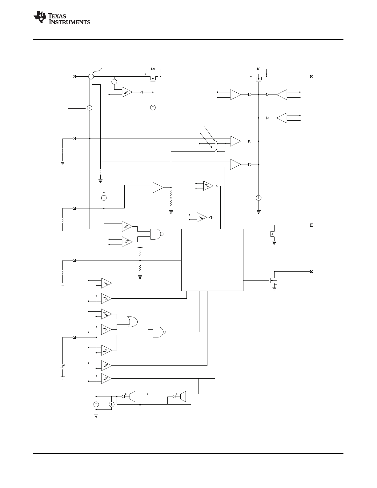
OUT
Charge
Pump
IN OUT
OUTREG
REF
TJ°C
125°C
REF
IN
IN
ISET
Charge
Pump
PRE-TERM
75mA
+
CHARGE
CONTROL
OUT
V
TERM_EN
ISET2 (LO=ISET,HI=USB500,
FLOAT =USB100)
V
COLD-FLT
V
HOT-45 C
o
V
TTDM
V
CE
TS
5 Am 45 Am
V
CLAMP
= 1.4V
ColdTemperature
SinkCurrent
=45 Am
LO =TTDMMODE
HI=CHIP DISABLE
OUT
CHG
ON:
OnDuring
1stChargeOnly
OFF:
+
Increasedfrom 75 A to85 A form m
1stminuteofcharge.
+
_
+
_
+
_
+
_
+
_
+
_
+
_
+
_
+
_
+
_
+
_
InternalCharge
CurrentSense
w/ MultipleOutputs
+
_
USBSense
Resistor
USB100/500
REF
+
_
1.5V
FASTCHARGE
PRE-CHARGE
PG
HI =SuspendCHG
V
COLD-10 C
o
V
HOT-FLT
+
_
+
_
HI =HalfCHG(JEITA)
HI =4.06Vreg(JEITA)
V
DISABLE
+
_
+
-
80 mV
Input
Power
Detect
+
_
IN-DPM
REF
0.9VFloat
TS - bq24090
+
_
Disable
SinkCurrent
=20 Am
Bq24090 isasshown
X2Gain(1:2)
Term:Pre-CHGX2
TermReference
Pre-CHGReference
I x1.5V
540 A
OUT
W
T C
J
o
+
_
150 C
ThermalShutdown
o
REF
IN
+
_
OVP
REF
www.ti.com
FUNCTIONAL BLOCK DIAGRAM
bq24090, bq24091
bq24092, bq24093
SLUS968B –JANUARY 2010–REVISED JUNE 2010
Copyright © 2010, Texas Instruments Incorporated Submit Documentation Feedback 9
Product Folder Link(s): bq24090 bq24091 bq24092 bq24093
Vin
Viset
Vchg
Vpg
t-time-20ms/div
2V/div
2V/div
5V/div
2V/div
Vin
Viset
Vchg
Vpg
t-time-100ms/div
2V/div
2V/div
2V/div
5V/div
Vts
Viset
Vchg
Vpg
t-time-50ms/div
2V/div
2V/div
2V/div
500mV/div
Vin
Vchg
Vpg
Vout
BatteryDetectMode
t-time-20ms/div
2V/div
5V/div
5V/div
2V/div
Vin
Viset
Vts
Vout
t-time-5ms/div
2V/div
2V/div
1V/div
500mV/div
Viset
Vchg
Vts
Vout
1BatteryDetectCycle
Entered TTDM
t-time-10ms/div
5V/div
1V/div
1V/div
1V/div
bq24090, bq24091
bq24092, bq24093
SLUS968B –JANUARY 2010–REVISED JUNE 2010
TYPICAL OPERATIONAL CHARACTERISTICS
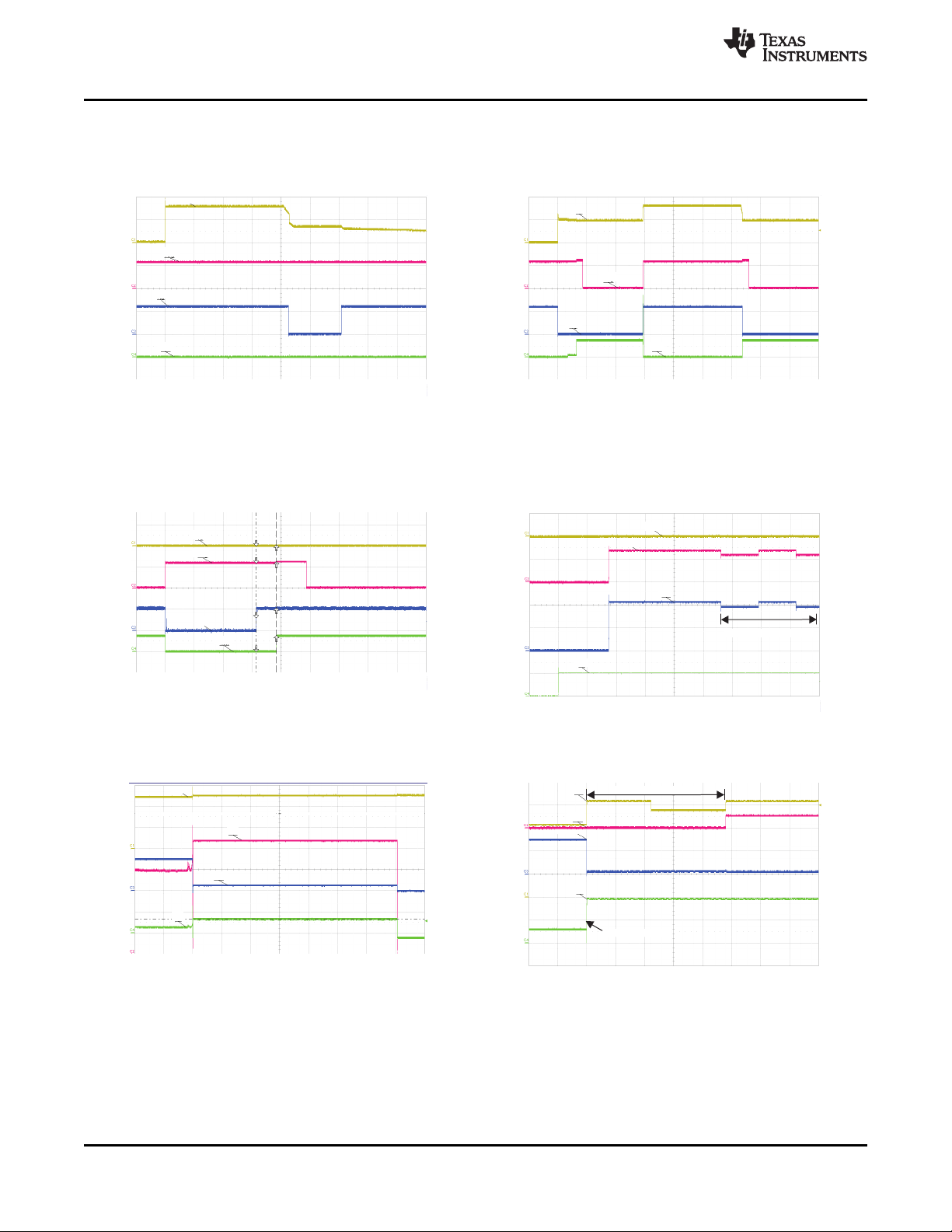
SETUP: bq2409x typical applications schematic; VIN= 5V, V
POWER UP, DOWN, OVP, DISABLE AND ENABLE WAVEFORMS
BAT
www.ti.com
= 3.6V (unless otherwise indicated)
Figure 1. OVP 8V Adaptor - Hot Plug Figure 2. OVP from Normal Power-up
Operation – VIN0V → 5V → 6.8V →5V
10kΩ resistor from TS to GND. 10kΩ is shorted to disable the IC.
Fixed 10kΩ resistor, between TS and GND.
Figure 3. TS Enable and Disable Figure 4. Hot Plug Source w/No Battery – Battery
Detection
Figure 5. Battery Removal – GND Removed 1st, 42 Ω Load Figure 6. Battery Removal with OUT and
TS Disconnect 1st, With 100 Ω Load
10 Submit Documentation Feedback Copyright © 2010, Texas Instruments Incorporated
Continuous battery detection when not in TTDM.
Product Folder Link(s): bq24090 bq24091 bq24092 bq24093
Viset
Vchg
V_0.1 _OUTW
Vout
BatteryDeclared Absent
t-time-20ms/div
100mV/div
1V/div
1V/div
5V/div
Viset
Vchg
Vout
V_0.1 _OUTW
Battery
Threshold
Reached
t-time-500ms/div
1V/div
5V/div
1V/div
100mV/div
Viset
Vchg
Vout
V_0.1 _OUTW
I ClampedCurrent
OUT
I ShortDetected
andLatchedOff
SET
t-time-200 s/divm
1V/div
2V/div
500mV/div
100mV/div
Vin
Viset
Vchg
V_0.1 _OUTW
t-time-1ms/div
2V/div
2V/div
20mV/div
500mV/div
Vin
Viset
Vchg
V_0.1 _OUTW
ShortDetectedin100mA
modeandLatchedOff
t-time-5ms/div
2V/div
2V/div
500mV/div
20mV/div
www.ti.com
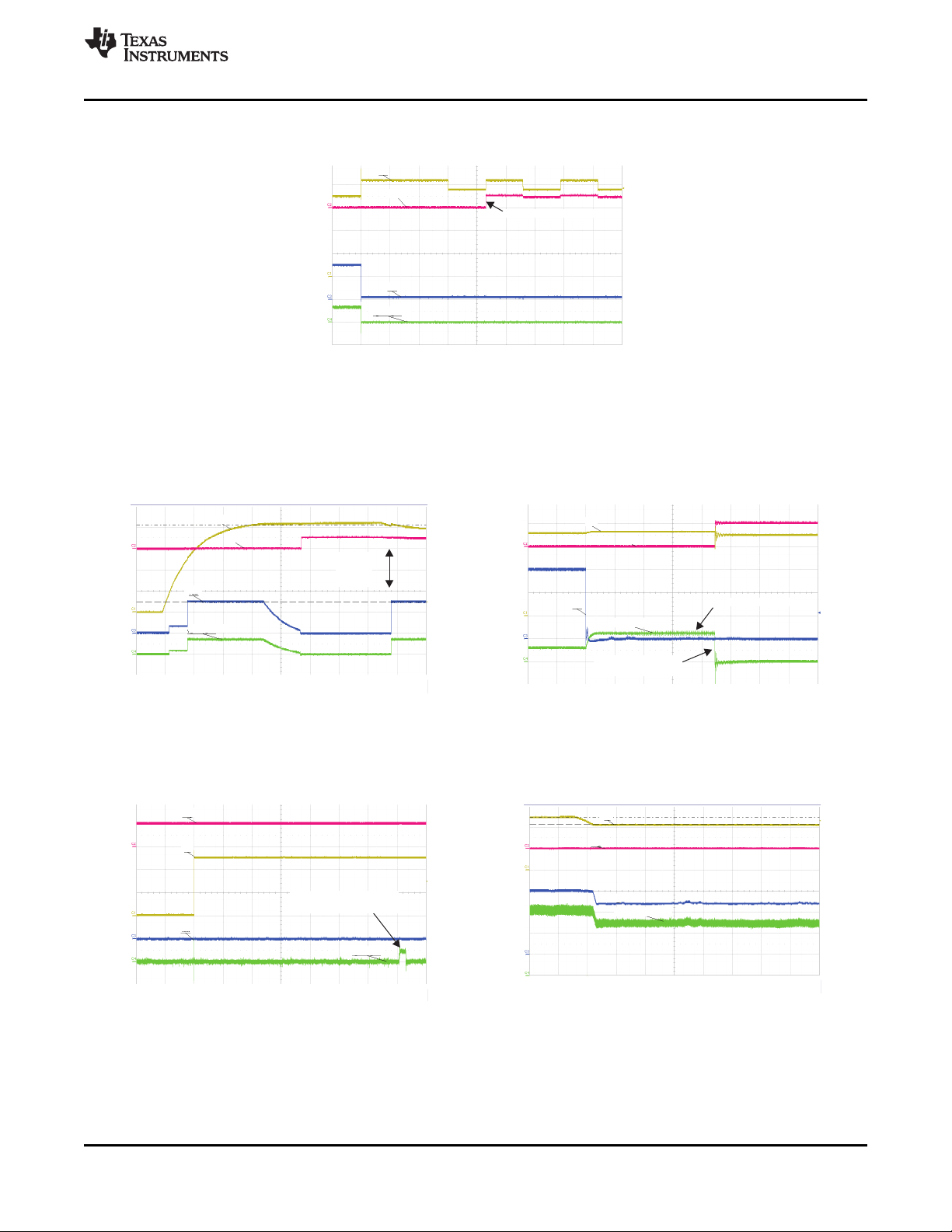
TYPICAL OPERATIONAL CHARACTERISTICS (continued)
SETUP: bq2409x typical applications schematic; VIN= 5V, V
Figure 7. Battery Removal with fixed TS = 0.5V
PROTECTION CIRCUITS WAVEFORMS
CH4: Iout (1A/Div)
Battery voltage swept from 0V to 4.25V to 3.9V.
CH4: Iout (1A/Div)
SLUS968B –JANUARY 2010–REVISED JUNE 2010
= 3.6V (unless otherwise indicated)
BAT
bq24090, bq24091
bq24092, bq24093
Figure 8. Battery Charge Profile Figure 9. ISET Shorted During Normal Operation
CH4: Iout (0.2A/Div)
CH4: Iout (0.2A/Div)
Figure 10. ISET Shorted Prior to USB Power-up Figure 11. DPM – Adaptor Current Limits – Vin Regulated
Copyright © 2010, Texas Instruments Incorporated Submit Documentation Feedback 11
The IC temperature rises to 125°C and enters thermal regulation. Charge current is reduced to regulate the IC at
125°C. VIN is reduced, the IC temperature drops, the charge current returns to the programmed value.
Product Folder Link(s): bq24090 bq24091 bq24092 bq24093

Vin
Viset
Vchg
V_0.1 _OUTW
t-time-500 s/divm
2V/div
2V/div
500mV/div
20mV/div
Viset
Vout
Vin
V_0.1 _OUTW
Exits
Thermal
Regulation
Enters
Thermal
Regulation
t-time-1s/div
2V/div
1V/div
1V/div
50mV/div
Vin
Viset
Vchg
Vpg
t-time-20ms/div
5V/div
5V/div
1V/div
1V/div
528
530
532
534
536
538
540
542
544
546
0 0.2 0.4 0.6 0.8
I -OutputCurrent- A
O
Kiset
Kiset- W
.15
LowtoHighCurrents
(mayoccurinrechargetofastchargetransion)
HightoLowCurrents
(mayoccurinVoltageRegulation- TaperCurrent)
4.196
4.198
4.2
4.202
4.204
4.206
4.208
4.21
4.212
4.5 5 5.5 6 6.5
R 100
OUT =
Ω
V @25°C
O
V @85°C
O
V -InputVoltageDC-V
I
V -OutputVoltageDC-V
OUT
V @0°C
O
4.192
4.193
4.194
4.195
4.196
4.197
4.198
4.199
4.2
0 0.2 0.4 0.6 0.8 1
I -Outputcurrent- A
O
V @0°C
reg
V -OutputVoltage-V
OUT
V @25°C
reg
V @85°C
reg
bq24090, bq24091
bq24092, bq24093
SLUS968B –JANUARY 2010–REVISED JUNE 2010
TYPICAL OPERATIONAL CHARACTERISTICS (continued)
SETUP: bq2409x typical applications schematic; VIN= 5V, V
= 3.6V (unless otherwise indicated)
BAT
www.ti.com
Figure 12. DPM – USB Current Limits – Vin Regulated to Figure 13. Thermal Reg. – Vin increases PWR/Iout
4.4V Reduced
VINswept from 5V to 3.9V to 5V, V
Figure 14. Entering and Exiting Sleep Mode Figure 15. K
BAT
= 4V
for Low and High Currents
ISET
12 Submit Documentation Feedback Copyright © 2010, Texas Instruments Incorporated
Figure 16. Line Regulation Figure 17. Load Regulation Over Temperature
Product Folder Link(s): bq24090 bq24091 bq24092 bq24093

361.8
362
362.2
362.4
362.6
362.8
363
363.2
363.4
2.5 3 3.5 4 4.5
V -OutputVoltage-V
O
I @0°C
O
I @85°C
O
I @25°C
O
I -OutputCurrent-mA
O
bq24090, bq24091
bq24092, bq24093
www.ti.com
TYPICAL OPERATIONAL CHARACTERISTICS (continued)
SETUP: bq2409x typical applications schematic; VIN= 5V, V
Figure 18. Current Regulation Over Temperature
= 3.6V (unless otherwise indicated)
BAT
FUNCTIONAL GENERAL DESCRIPTION
The bq2409x is a highly integrated family of 5x3mm2single cell Li-Ion chargers. The charger can be used to
charge a battery, power a system or both. The charger has three phases of charging: Pre-charge to recover a
fully discharged battery, fast-charge constant current to supply the buck charge safely and voltage regulation to
safely reach full capacity. The charger is very flexible, allowing programming of the fast-charge current and
Pre-charge/Termination Current. This charger is designed to work with a USB connection or Adaptor (DC out).
The charger also checks to see if a battery is present.
The charger also comes with a full set of safety features: JEITA Temperature Standard, Over-Voltage Protection,
DPM-IN, Safety Timers, and ISET short protection. All of these features and more are described in detail below.
The charger is designed for a single power path from the input to the output to charge a single cell Li-Ion battery
pack. Upon application of a 5VDC power source the ISET and OUT short checks are performed to assure a
proper charge cycle.
If the battery voltage is below the LOWV threshold, the battery is considered discharged and a preconditioning
cycle begins. The amount of precharge current can be programmed using the PRE-TERM pin which programs a
percent of fast charge current (10 to 100%) as the precharge current. This feature is useful when the system load
is connected across the battery “stealing” the battery current. The precharge current can be set higher to account
for the system loading while allowing the battery to be properly conditioned. The PRE-TERM pin is a dual
function pin which sets the precharge current level and the termination threshold level. The termination "current
threshold" is always half of the precharge programmed current level.
Once the battery voltage has charged to the V
is applied. The fast charge constant current is programmed using the ISET pin. The constant current provides the
bulk of the charge. Power dissipation in the IC is greatest in fast charge with a lower battery voltage. If the IC
reaches 125°C the IC enters thermal regulation, slows the timer clock by half and reduce the charge current as
needed to keep the temperature from rising any further. Figure 19 shows the charging profile with thermal
regulation. Typically under normal operating conditions, the IC’s junction temperature is less than 125°C and
thermal regulation is not entered.
Once the cell has charged to the regulation voltage the voltage loop takes control and holds the battery at the
regulation voltage until the current tapers to the termination threshold. The termination can be disabled if desired.
The CHG pin is low (LED on) during the first charge cycle only and turns off once the termination threshold is
reached, regardless if termination, for charge current, is enabled or disabled.
Further details are mentioned in the Operating Modes section.
threshold, fast charge is initiated and the fast charge current
LOWV
SLUS968B –JANUARY 2010–REVISED JUNE 2010
Copyright © 2010, Texas Instruments Incorporated Submit Documentation Feedback 13
Product Folder Link(s): bq24090 bq24091 bq24092 bq24093

PRE-CHARGE
CURRENT AND
TERMINATION
THRESHOLD
FAST-CHARGE
CURRENT
T
(PRECHG)
Charge
Complete
Status,
Charger
Off
Pre-
Conditioning
Phase
Current
Regulation
Phase
VoltageRegulationand
ChargeTermination
Phase
Battery
Voltage,
V
(OUT)
BatteryCurrent,
I
(OUT)
DONE
0A
Thermal
Regulation
Phase
Temperature, Tj
I
O(OUT)
T
(THREG)
I
(TERM)
I
O(PRECHG)
V
O(REG)
V
O(LOWV)
DONE
T
(CHG)
bq24090, bq24091
bq24092, bq24093
SLUS968B –JANUARY 2010–REVISED JUNE 2010
FUNCTIONAL GENERAL DESCRIPTION (continued)
www.ti.com
Figure 19. Charging Profile With Thermal Regulation
14 Submit Documentation Feedback Copyright © 2010, Texas Instruments Incorporated
Product Folder Link(s): bq24090 bq24091 bq24092 bq24093

bq24090, bq24091
bq24092, bq24093
www.ti.com
DETAILED FUNCTIONAL DESCRIPTION
Power-Down or Undervoltage Lockout (UVLO)
The bq2409x family is in power down mode if the IN pin voltage is less than UVLO. The part is considered
“dead” and all the pins are high impedance. Once the IN voltage rises above the UVLO threshold the IC will
enter Sleep Mode or Active mode depending on the OUT pin (battery) voltage.
Under Voltage Lockout (UVLO):
The bq2409x family is in power down mode if the IN pin voltage is less than V
and all the pins are high impedance.
Power-up
The IC is alive after the IN voltage ramps above UVLO (see sleep mode), resets all logic and timers, and starts
to perform many of the continuous monitoring routines. Typically the input voltage quickly rises through the
UVLO and sleep states where the IC declares power good, starts the qualification charge at 100mA, sets the
input current limit threshold base on the ISET2 pin, starts the safety timer and enables the CHG pin. See
Figure 20.
Sleep Mode
If the IN pin voltage is between than V
OUT+VDT
counting stops (not reset) and the PG and CHG pins are high impedance. As the input voltage rises and the
charger exits sleep mode, the PG pin goes low, the safety timer continues to count, charge is enabled and the
CHG pin returns to its previous state. See Figure 21
and UVLO, the charge current is disabled, the safety timer
SLUS968B –JANUARY 2010–REVISED JUNE 2010
. The part is considered “dead”
UVLO
New Charge Cycle
A new charge cycle is started when a good power source is applied, performing a chip disable/enable (TS pin),
exiting Termination and Timer Disable Mode (TTDM), detecting a battery insertion or the OUT voltage dropping
below the V
a dropping below V
threshold. The CHG pin is active low only during the first charge cycle, therefore exiting TTDM or
RCH
will not turn on the CHG pin FET, if the CHG pin is already high impedance.
RCH
Copyright © 2010, Texas Instruments Incorporated Submit Documentation Feedback 15
Product Folder Link(s): bq24090 bq24091 bq24092 bq24093

LDO
V
SS
1.8V
0V
LDO
HYS
0°C
0°C
HYS
10°C
10°C
HYS
45°C
45°C
HYS
60°C
60°C
HYS
EN
DIS
HYS
t
DGL(TS)
t
DGL(TS)
t
DGL(TS)
t
DGL(TS)
t
DGL(TS_IOC)
Rising
t
DGL(TS_IOC)
Falling
t
DGL(TS)
t
DGL(TS)
t
DGL(TTDM)
Exit
t
DGL(TTDM)
Enter
t<t
DGL(TTDM)
Exit
t<t
DGL(IS)
Normal
Operation
LDO
Mode
Normal
Operation
Cold
Operation
Cold
Fault
LDO
Mode
Cold
Fault
Normal
Operation
t
DGL(TS)
t
DGL(TTDM)
Enter
Disabled
Cold
Operation
HOT
Fault
4.06V
HOT
Operation
Normal
Operation
4.06V
HOT
Operation
Disabled
t
DGL(TS1_IOC)
ColdtoNormal
DrawingNottoScale
DotsShow Threshold TripPoints
fllowedbyadeglitchtimebefore
transitioningintoanewmode.
t
bq24090, bq24091
bq24092, bq24093
SLUS968B –JANUARY 2010–REVISED JUNE 2010
www.ti.com
16 Submit Documentation Feedback Copyright © 2010, Texas Instruments Incorporated
Figure 20. TS Battery Temperature Bias Threshold and Deglitch Timers
Product Folder Link(s): bq24090 bq24091 bq24092 bq24093

ApplyInput
Power
SetInputCurrentLimitto 100 mA
andStartCharge
PerformISET & OUT shorttests
RememberISET2 State
Setchargecurrent
basedonISET2 truth
table.
Returnto
Charge
Ispowergood?
V
BAT+VDT
< VIN< V
OVP
& V
UVLO
< V
IN
No
Yes
Ischipenabled?
VTS> V
EN
No
Yes
TurnonPGFET
PGpinLOW
www.ti.com
bq24090, bq24091
bq24092, bq24093
SLUS968B –JANUARY 2010–REVISED JUNE 2010
Overvoltage-Protection (OVP) – Continuously Monitored
If the input source applies an overvoltage, the pass FET, if previously on, turns off after a deglitch, t
timer ends and the CHG and PG pin goes to a high impedance state. Once the overvoltage returns to a normal
voltage, the PG pin goes low, timer continues, charge continues and the CHG pin goes low after a 25ms
deglitch. PG pin is optional on some packages
Figure 21. bq2409x Power-Up Flow Diagram
BLK(OVP)
. The
Copyright © 2010, Texas Instruments Incorporated Submit Documentation Feedback 17
Product Folder Link(s): bq24090 bq24091 bq24092 bq24093

bq24090, bq24091
bq24092, bq24093
SLUS968B –JANUARY 2010–REVISED JUNE 2010
Power Good Indication (PG)
After application of a 5V source, the input voltage rises above the UVLO and sleep thresholds (VIN>V
but is less than OVP (VIN<V
,), then the PG FET turns on and provides a low impedance path to ground. See
OVP
Figure 1, Figure 2, and Figure 14.
CHG Pin Indication
The charge pin has an internal open drain FET which is on (pulls down to VSS) during the first charge only
(independent of TTDM) and is turned off once the battery reaches voltage regulation and the charge current
tapers to the termination threshold set by the PRE-TERM resistor.
The charge pin is high impedance in sleep mode and OVP (if PG is high impedance) and return to its previous
state once the condition is removed.
Cycling input power, pulling the TS pin low and releasing or entering pre-charge mode causes the CHG pin to go
reset (go low if power is good and a discharged battery is attached) and is considered the start of a first charge.
CHG and PG LED Pull-up Source
For host monitoring, a pull-up resistor is used between the "STATUS" pin and the VCCof the host and for a visual
indication a resistor in series with an LED is connected between the "STATUS" pin and a power source. If the
CHG or PG source is capable of exceeding 7V, a 6.2V Zener should be used to clamp the voltage. If the source
is the OUT pin, note that as the battery changes voltage, the brightness of the LEDs vary.
www.ti.com
BAT+VDT
),
Charging State CHG FET/LED
1st Charge ON
Refresh Charge
OVP OFF
SLEEP
TEMP FAULT ON for 1st Charge
VINPower Good State PG FET/LED
UVLO
SLEEP Mode OFF
OVP Mode
IN-DPM (V
IN-DPM
Normal Input (V
or IN–DPM)
+ VDT< VIN<
OUT
V
)
OUP
PG is independent of chip disable
ON
The IN-DPM feature is used to detect an input source voltage that is folding back (voltage dropping), reaching its
current limit due to excessive load. When the input voltage drops to the V
threshold the internal pass FET
IN-DPM
starts to reduce the current until there is no further drop in voltage at the input. This would prevent a source with
voltage less than V
to power the out pin. This works well with current limited adaptors and USB ports as
IN-DPM
long as the nominal voltage is above 4.3V and 4.4V respectively. This is an added safety feature that helps
protect the source from excessive loads.
OUT
The Charger’s OUT pin provides current to the battery and to the system, if present. This IC can be used to
charge the battery plus power the system, charge just the battery or just power the system (TTDM) assuming the
loads do not exceed the available current. The OUT pin is a current limited source and is inherently protected
against shorts. If the system load ever exceeds the output programmed current threshold, the output will be
discharged unless there is sufficient capacitance or a charged battery present to supplement the excessive load.
18 Submit Documentation Feedback Copyright © 2010, Texas Instruments Incorporated
Product Folder Link(s): bq24090 bq24091 bq24092 bq24093

0
0.5
1
1.5
2
2.5
3
3.5
4
4.5
0.6
1.8
V -Voltage-V
TS
NormalizedOUTCurrentandV -V
REG
60 Cto45 C
HOT TEMP
4.06V
Regulation
o o
I
OUT
V
OUT
0
0.2
0.4
0.8
1
1.2
1.4
1.6
For<45 C,4.2VRegulation
o
} HotFault
NoOperation
DuringCold
Fault
Cold
Fault
ICDisable}
0 C
o
< 48 C
o
60 C
o
10 C
o
100%ofProgrammed
Current
50%
Termination
Disable
bq24090, bq24091
bq24092, bq24093
www.ti.com
ISET
An external resistor is used to Program the Output Current (50 to 800mA) and can be used as a current monitor.
R
= K
ISET
ISET
÷ I
OUT
Where:
I
is the desired fast charge current;
OUT
K
is a gain factor found in the electrical specification
ISET
For greater accuracy at lower currents, part of the sense FET is disabled to give better resolution. Figure 15
shows the transition from low current to higher current. Going from higher currents to low currents, there is
hysteresis and the transition occurs around 0.15A.
The ISET resistor is short protected and will detect a resistance lower than ≉340Ω. The detection requires at
least 80mA of output current. If a “short” is detected, then the IC will latch off and can only be reset by cycling the
power. The OUT current is internally clamped to a maximum current between 1.1A and 1.35A and is independent
of the ISET short detection circuitry, as shown in Figure 23. Also, see Figure 9 and Figure 10.
(1) (1)
SLUS968B –JANUARY 2010–REVISED JUNE 2010
Figure 22. Operation Over TS Bias Voltage
Copyright © 2010, Texas Instruments Incorporated Submit Documentation Feedback 19
Product Folder Link(s): bq24090 bq24091 bq24092 bq24093

0
0.2
0.4
0.6
0.8
1
1.2
1.4
1.6
1.8
100
1000
10 000
I -
SET
W
I -OutputCurrent- A
O
I InternalClampRange
OUT
I Short
Fault
Range
SET
NonRestricted
Operating Area
I Programmed
OUT
min
max
I Clampmin-max
OUT
I Faultmin-max
OUT
Drive
Logic
V
CC
To
ISET2
R1
R2
ToISET2
V
CC
Q1
Q2
Drive
Logic
R1Divider
setto0.9V
Whichisthe
FloatVoltage
OR
bq24090, bq24091
bq24092, bq24093
SLUS968B –JANUARY 2010–REVISED JUNE 2010
www.ti.com
Figure 23. Programmed/Clamped Out Current
PRE_TERM – Pre-Charge and Termination Programmable Threshold
Pre-Term is used to program both the pre-charge current and the termination current threshold. The pre-charge
current level is a factor of two higher than the termination current level. The termination can be set between 5%
and 50% of the programmed output current level set by ISET. If left floating the termination and pre-charge are
set internally at 10/20% respectively. The pre-charge-to-fast-charge, V
R
PRE-TERM
= %Term × K
= %Pre-CHG × K
TERM
PRE-CHG
threshold is set to 2.5V.
lowv
(2) (2)
Where:
%Term is the percent of fast charge current where termination occurs;
%Pre-CHG is the percent of fast charge current that is desired during precharge;
K
TERM
and K
PRE-CHG
are gain factors found in the electrical specifications.
ISET2
Is a 3-state input and programs the Input Current Limit/Regulation Threshold. A low will program a regulated fast
charge current via the ISET resistor and is the maximum allowed input/output current for any ISET2 setting, Float
will program a 100mA Current limit and High will program a 500mA Current limit.
Below are two configurations for driving the 3-state ISET2 pin:
20 Submit Documentation Feedback Copyright © 2010, Texas Instruments Incorporated
Product Folder Link(s): bq24090 bq24091 bq24092 bq24093

bq24090, bq24091
bq24092, bq24093
www.ti.com
TS
The TS pin is designed to follow the new JEITA temperature standard for Li-Ion batteries. There are now four
thresholds, 60°C, 45°C, 10°C, and 0°C. Normal operation occurs between 10°C and 45°C. If between 0°C and
10°C the charge current level is cut in half and if between 45°C and 60°C the regulation voltage is reduced to
4.1Vmax, see Figure 22. The TS feature is implemented using an internal 50mA current source to bias the
thermistor (designed for use with a 10k NTC b = 3370 (SEMITEC 103AT-2 or Mitsubishi TH05-3H103F)
connected from the TS pin to VSS. If this feature is not needed, a fixed 10k can be placed between TS and VSSto
allow normal operation. This may be done if the host is monitoring the thermistor and then the host would
determine when to pull the TS pin low to disable charge.
The TS pin has two additional features, when the TS pin is pulled low or floated/driven high. A low disables
charge (similar to a high on the BAT_EN feature) and a high puts the charger in TTDM.
Above 60°C or below 0°C the charge is disabled. Once the thermistor reaches ≈–10°C the TS current folds back
to keep a cold thermistor (between –10°C and –50°C) from placing the IC in the TTDM mode. If the TS pin is
pulled low into disable mode, the current is reduced to ≈30mA, see Figure 20. Since the ITScurrent is fixed along
with the temperature thresholds, it is not possible to use thermistor values other than the 10k NTC (at 25°C).
For non-JEITA spins, the operating range is between 0°C and 45°C.
Termination and Timer Disable Mode (TTDM) -TS pin high
The battery charger is in TTDM when the TS pin goes high from removing the thermistor (removing battery
pack/floating the TS pin) or by pulling the TS pin up to the TTDM threshold.
When entering TTDM, the 10 hour safety timer is held in reset and termination is disabled. A battery detect
routine is run to see if the battery was removed or not. If the battery was removed then the CHG pin will go to its
high impedance state if not already there. If a battery is detected the CHG pin does not change states until the
current tapers to the termination threshold, where the CHG pin goes to its high impedance state if not already
there (the regulated output will remain on).
The charging profile does not change (still has pre-charge, fast-charge constant current and constant voltage
modes). This implies the battery is still charged safely and the current is allowed to taper to zero.
When coming out of TTDM, the battery detect routine is run and if a battery is detected, then a new charge cycle
begins and the CHG LED turns on.
SLUS968B –JANUARY 2010–REVISED JUNE 2010
If TTDM is not desired upon removing the battery with the thermistor, one can add a 237k resistor between TS
and VSSto disable TTDM. This keeps the current source from driving the TS pin into TTDM. This creates ≈0.1°C
error at hot and a ≈3°C error at cold.
Timers
The pre-charge timer is set to 30 minutes. The pre-charge current, can be programmed to off-set any system
load, making sure that the 30 minutes is adequate.
The fast charge timer is fixed at 10 hours and can be increased real time by going into thermal regulation,
IN-DPM or if in USB current limit. The timer clock slows by a factor of 2, resulting in a clock than counts half as
fast when in these modes. If either the 30 minute or ten hour timer times out, the charging is terminated and the
CHG pin goes high impedance if not already in that state. The timer is reset by disabling the IC, cycling power or
going into and out of TTDM.
Termination
Once the OUT pin goes above VRCH, (reaches voltage regulation) and the current tapers down to the
termination threshold, the CHG pin goes high impedance and a battery detect route is run to determine if the
battery was removed or the battery is full. If the battery is present, the charge current will terminate. If the battery
was removed along with the thermistor, then the TS pin is driven high and the charge enters TTDM. If the battery
was removed and the TS pin is held in the active region, then the battery detect routine will continue until a
battery is inserted.
Copyright © 2010, Texas Instruments Incorporated Submit Documentation Feedback 21
Product Folder Link(s): bq24090 bq24091 bq24092 bq24093

bq24090, bq24091
bq24092, bq24093
SLUS968B –JANUARY 2010–REVISED JUNE 2010
Battery Detect Routine
The battery detect routine should check for a missing battery while keeping the OUT pin at a useable voltage.
Whenever the battery is missing the CHG pin should be high impedance.
The battery detect routine is run when entering and exiting TTDM to verify if battery is present, or run all the time
if battery is missing and not in TTDM. On power-up, if battery voltage is greater than V
threshold, a battery
RCH
detect routine is run to determine if a battery is present.
The battery detect routine is disabled while the IC is in TTDM, or has a TS fault. See Figure 24 for the Battery
Detect Flow Diagram.
Refresh Threshold
After termination, if the OUT pin voltage drops to V
but the CHG pin remains at a high impedance (off).
(100mV below regulation) then a new charge is initiated,
RCH
Starting a Charge on a Full Battery
The termination threshold is raised by ≉14%, for the first minute of a charge cycle so if a full battery is removed
and reinserted or a new charge cycle is initiated, that the new charge terminates (less than 1 minute). Batteries
that have relaxed many hours may take several minutes to taper to the termination threshold and terminate
charge.
www.ti.com
22 Submit Documentation Feedback Copyright © 2010, Texas Instruments Incorporated
Product Folder Link(s): bq24090 bq24091 bq24092 bq24093

Start
BATT_DETECT
Start 25mstimer
TimerExpired?
IsVOUT<VREG-100mV?
BatteryPresent
TurnoffSinkCurrent
Returntoflow
SetOUT REG
toVREG-400mV
Enablesinkcurrent
Reset & Start 25mstimer
No
Yes
TimerExpired?
No
Yes
IsVOUT>VREG-300mV?
BatteryPresent
TurnoffSinkCurrent
Returntoflow
Yes
No
Yes
No
Battery Absent
Don’tSignalCharge
TurnoffSinkCurrent
ReturntoFlow
www.ti.com
bq24090, bq24091
bq24092, bq24093
SLUS968B –JANUARY 2010–REVISED JUNE 2010
Figure 24. Battery Detect Routine
Copyright © 2010, Texas Instruments Incorporated Submit Documentation Feedback 23
Product Folder Link(s): bq24090 bq24091 bq24092 bq24093

BatteryPack
VBUS
GND
D+
D-
USBPort
DC+
GND
Adaptor
VDD
D-
D+
GND
TTDM
Host
SystemLoad
OR
ISET/100/500 mA
1
2
3
4
5
10
9
8
7
6
IN
ISET
VSS
PRETERM
PG
NC
ISET2
CHG
TS
OUT
bq24090
+
+
1 Fm
1 Fm
1kW
1.5kW
1.5kW
2kW
bq24090, bq24091
bq24092, bq24093
SLUS968B –JANUARY 2010–REVISED JUNE 2010
bq24090 CHARGER APPLICATION DESIGN EXAMPLE
www.ti.com
Requirements
• Supply voltage = 5 V
• Fast charge current: I
• Termination Current Threshold: %
= 540 mA; ISET-pin 2
OUT-FC
IOUT-FC
= 10% of Fast Charge or ~54mA
• Pre-Charge Current by default is twice the termination Current or ~108mA
• TS – Battery Temperature Sense = 10k NTC (103AT)
Calculations
Program the Fast Charge Current, ISET:
R
= [K
ISET
from electrical characteristics table. . . K
R
= [540AΩ/0.54A] = 1.0 kΩ
ISET
Selecting the closest standard value, use a 1 kΩ resistor between ISET (pin 16) and VSS.
Program the Termination Current Threshold, ITERM:
R
PRE-TERM
R
PRE-TERM
Selecting the closest standard value, use a 2 kΩ resistor between ITERM (pin 15) and Vss.
One can arrive at the same value by using 20% for a pre-charge value (factor of 2 difference).
R
PRE-TERM
R
PRE-TERM
TS Function
Use a 10k NTC thermistor in the battery pack (103AT).
To Disable the temp sense function, use a fixed 10k resistor between the TS (Pin 1) and Vss.
24 Submit Documentation Feedback Copyright © 2010, Texas Instruments Incorporated
/ I
(ISET)
= K
(TERM)
(OUT)
]
× %
IOUT-FC
= 200Ω/% × 10% = 2kΩ
= K
(PRE-CHG)
× %
IOUT-FC
= 100Ω/% × 20%= 2kΩ
= 540AΩ
(SET)
Product Folder Link(s): bq24090 bq24091 bq24092 bq24093

bq24090, bq24091
bq24092, bq24093
www.ti.com
CHG and PG
LED Status: connect a 1.5k resistor in series with a LED between the OUT pin and the CHG pin.
Connect a 1.5k resistor in series with a LED between the OUT pin and the and PG pin.
Processor Monitoring: Connect a pull-up resistor between the processor’s power rail and the CHG pin.
Connect a pull-up resistor between the processor’s power rail and the PG pin.
SELECTING IN AND OUT PIN CAPACITORS
In most applications, all that is needed is a high-frequency decoupling capacitor (ceramic) on the power pin, input
and output pins. Using the values shown on the application diagram, is recommended. After evaluation of these
voltage signals with real system operational conditions, one can determine if capacitance values can be adjusted
toward the minimum recommended values (DC load application) or higher values for fast high amplitude pulsed
load applications. Note if designed for high input voltage sources (bad adaptors or wrong adaptors), the capacitor
needs to be rated appropriately. Ceramic capacitors are tested to 2x their rated values so a 16V capacitor may
be adequate for a 30V transient (verify tested rating with capacitor manufacturer).
THERMAL PACKAGE
The bq2409x family is packaged in a thermally enhanced MSOP package. The package includes a thermal pad
to provide an effective thermal contact between the IC and the printed circuit board (PCB). The power pad
should be directly connected to the VSS pin. Full PCB design guidelines for this package are provided in the
application note entitled: Power Pad Thermally Enhanced Package Note (SLMA002). The most common
measure of package thermal performance is thermal impedance (qJA) measured (or modeled) from the chip
junction to the air surrounding the package surface (ambient). The mathematical expression for qJAis:
q
= (TJ– T) / P (3) (3)
JA
Where:
TJ= chip junction temperature
T = ambient temperature
P = device power dissipation
Factors that can influence the measurement and calculation of qJAinclude:
1. Whether or not the device is board mounted
2. Trace size, composition, thickness, and geometry
3. Orientation of the device (horizontal or vertical)
4. Volume of the ambient air surrounding the device under test and airflow
5. Whether other surfaces are in close proximity to the device being tested
Due to the charge profile of Li-Ion batteries the maximum power dissipation is typically seen at the beginning of
the charge cycle when the battery voltage is at its lowest. Typically after fast charge begins the pack voltage
increases to ≉3.4V within the first 2 minutes. The thermal time constant of the assembly typically takes a few
minutes to heat up so when doing maximum power dissipation calculations, 3.4V is a good minimum voltage to
use. This is verified, with the system and a fully discharged battery, by plotting temperature on the bottom of the
PCB under the IC (pad should have multiple vias), the charge current and the battery voltage as a function of
time. The fast charge current will start to taper off if the part goes into thermal regulation.
The device power dissipation, P, is a function of the charge rate and the voltage drop across the internal
PowerFET. It can be calculated from the following equation when a battery pack is being charged :
P = [V
The thermal loop feature reduces the charge current to limit excessive IC junction temperature. It is
recommended that the design not run in thermal regulation for typical operating conditions (nominal input voltage
and nominal ambient temperatures) and use the feature for non typical situations such as hot environments or
higher than normal input source voltage. With that said, the IC will still perform as described, if the thermal loop
is always active.
(IN)
– V
(OUT)
] × I
(OUT)
+ [V
(OUT)
– V
(BAT)
] × I
(BAT)
SLUS968B –JANUARY 2010–REVISED JUNE 2010
(3)
Copyright © 2010, Texas Instruments Incorporated Submit Documentation Feedback 25
Product Folder Link(s): bq24090 bq24091 bq24092 bq24093

bq24090, bq24091
bq24092, bq24093
SLUS968B –JANUARY 2010–REVISED JUNE 2010
Leakage Current Effects on Battery Capacity
To determine how fast a leakage current on the battery will discharge the battery is an easy calculation. The time
from full to discharge can be calculated by dividing the Amp-Hour Capacity of the battery by the leakage current.
For a 0.75AHr battery and a 10mA leakage current (750mAHr/0.010mA = 75000 Hours), it would take 75k hours
or 8.8 years to discharge. In reality the self discharge of the cell would be much faster so the 10mA leakage
would be considered negligible.
Layout Tips
To obtain optimal performance, the decoupling capacitor from IN to GND (thermal pad) and the output filter
capacitors from OUT to GND (thermal pad) should be placed as close as possible to the bq2409x, with short
trace runs to both IN, OUT and GND (thermal pad).
• All low-current GND connections should be kept separate from the high-current charge or discharge paths
from the battery. Use a single-point ground technique incorporating both the small signal ground path and the
power ground path.
• The high current charge paths into IN pin and from the OUT pin must be sized appropriately for the maximum
charge current in order to avoid voltage drops in these traces
• The bq2409x family is packaged in a thermally enhanced MLP package. The package includes a thermal pad
to provide an effective thermal contact between the IC and the printed circuit board (PCB); this thermal pad is
also the main ground connection for the device. Connect the thermal pad to the PCB ground connection. It is
best to use multiple 10mil vias in the power pad of the IC and in close proximity to conduct the heat to the
bottom ground plane. The bottom ground place should avoid traces that “cut off” the thermal path. The thinner
the PCB the less temperature rise. The EVM PCB has a thickness of 0.031 inches and uses 2 oz. (2.8mil
thick) copper on top and bottom, and is a good example of optimal thermal performance.
SPACER
www.ti.com
REVISION HISTORY
Changes from Original (January 2010) to Revision A Page
• Changed V
• Changed I
• Changed V
Changes from Revision A (February 2010) to Revision B Page
• Changed the device number on the front page circuit From: bq24090 To: bq2409x ........................................................... 1
• Changed the ORDERING INFORMATION table Marking column From: Product Preview To: bq24092 and bq24093 ...... 2
DO(IN-OUT)
PRE-TERM
CLAMP(TS)
, MAX value From: 500 mV To: 520 mV in the Elect Characteristics table .......................................... 4
MAX value From: 79 µA to 81µA in the Elect Characteristics table ....................................................... 4
MIN value From: 1900 mV to 1800 mV in the Elect Characteristics table ........................................... 5
26 Submit Documentation Feedback Copyright © 2010, Texas Instruments Incorporated
Product Folder Link(s): bq24090 bq24091 bq24092 bq24093

PACKAGE OPTION ADDENDUM
www.ti.com
10-Jun-2010
PACKAGING INFORMATION
Orderable Device
BQ24090DGQR ACTIVE MSOP-
BQ24090DGQT ACTIVE MSOP-
BQ24091DGQR ACTIVE MSOP-
BQ24091DGQT ACTIVE MSOP-
BQ24092DGQR ACTIVE MSOP-
BQ24092DGQT ACTIVE MSOP-
BQ24093DGQR ACTIVE MSOP-
BQ24093DGQT ACTIVE MSOP-
(1)
The marketing status values are defined as follows:
ACTIVE: Product device recommended for new designs.
LIFEBUY: TI has announced that the device will be discontinued, and a lifetime-buy period is in effect.
NRND: Not recommended for new designs. Device is in production to support existing customers, but TI does not recommend using this part in a new design.
PREVIEW: Device has been announced but is not in production. Samples may or may not be available.
OBSOLETE: TI has discontinued the production of the device.
Status
(1)
Package Type Package
PowerPAD
PowerPAD
PowerPAD
PowerPAD
PowerPAD
PowerPAD
PowerPAD
PowerPAD
Drawing
Pins Package Qty
DGQ 10 2500 Green (RoHS
DGQ 10 250 Green (RoHS
DGQ 10 2500 Green (RoHS
DGQ 10 250 Green (RoHS
DGQ 10 2500 Green (RoHS
DGQ 10 250 Green (RoHS
DGQ 10 2500 Green (RoHS
DGQ 10 250 Green (RoHS
Eco Plan
& no Sb/Br)
& no Sb/Br)
& no Sb/Br)
& no Sb/Br)
& no Sb/Br)
& no Sb/Br)
& no Sb/Br)
& no Sb/Br)
(2)
Lead/
Ball Finish
CU NIPDAU Level-1-260C-UNLIM Purchase Samples
CU NIPDAU Level-1-260C-UNLIM Request Free Samples
CU NIPDAU Level-1-260C-UNLIM Purchase Samples
CU NIPDAU Level-1-260C-UNLIM Request Free Samples
CU NIPDAU Level-1-260C-UNLIM Purchase Samples
CU NIPDAU Level-1-260C-UNLIM Request Free Samples
CU NIPDAU Level-1-260C-UNLIM Purchase Samples
CU NIPDAU Level-1-260C-UNLIM Request Free Samples
MSL Peak Temp
(3)
Samples
(Requires Login)
(2)
Eco Plan - The planned eco-friendly classification: Pb-Free (RoHS), Pb-Free (RoHS Exempt), or Green (RoHS & no Sb/Br) - please check http://www.ti.com/productcontent for the latest availability
information and additional product content details.
TBD: The Pb-Free/Green conversion plan has not been defined.
Pb-Free (RoHS): TI's terms "Lead-Free" or "Pb-Free" mean semiconductor products that are compatible with the current RoHS requirements for all 6 substances, including the requirement that
lead not exceed 0.1% by weight in homogeneous materials. Where designed to be soldered at high temperatures, TI Pb-Free products are suitable for use in specified lead-free processes.
Pb-Free (RoHS Exempt): This component has a RoHS exemption for either 1) lead-based flip-chip solder bumps used between the die and package, or 2) lead-based die adhesive used between
the die and leadframe. The component is otherwise considered Pb-Free (RoHS compatible) as defined above.
Green (RoHS & no Sb/Br): TI defines "Green" to mean Pb-Free (RoHS compatible), and free of Bromine (Br) and Antimony (Sb) based flame retardants (Br or Sb do not exceed 0.1% by weight
in homogeneous material)
(3)
MSL, Peak Temp. -- The Moisture Sensitivity Level rating according to the JEDEC industry standard classifications, and peak solder temperature.
Addendum-Page 1

PACKAGE OPTION ADDENDUM
www.ti.com
Important Information and Disclaimer:The information provided on this page represents TI's knowledge and belief as of the date that it is provided. TI bases its knowledge and belief on information
provided by third parties, and makes no representation or warranty as to the accuracy of such information. Efforts are underway to better integrate information from third parties. TI has taken and
continues to take reasonable steps to provide representative and accurate information but may not have conducted destructive testing or chemical analysis on incoming materials and chemicals.
TI and TI suppliers consider certain information to be proprietary, and thus CAS numbers and other limited information may not be available for release.
10-Jun-2010
In no event shall TI's liability arising out of such information exceed the total purchase price of the TI part(s) at issue in this document sold by TI to Customer on an annual basis.
Addendum-Page 2

PACKAGE MATERIALS INFORMATION
www.ti.com 20-Jul-2010
TAPE AND REEL INFORMATION
*All dimensions are nominal
Device Package
BQ24090DGQR MSOP-
BQ24090DGQT MSOP-
BQ24091DGQR MSOP-
BQ24091DGQT MSOP-
BQ24092DGQR MSOP-
Type
Power
PAD
Power
PAD
Power
PAD
Power
PAD
Power
PAD
Package
Drawing
DGQ 10 2500 330.0 12.4 5.3 3.3 1.3 8.0 12.0 Q1
DGQ 10 250 180.0 12.4 5.3 3.3 1.3 8.0 12.0 Q1
DGQ 10 2500 330.0 12.4 5.3 3.3 1.3 8.0 12.0 Q1
DGQ 10 250 180.0 12.4 5.3 3.3 1.3 8.0 12.0 Q1
DGQ 10 2500 330.0 12.4 5.3 3.3 1.3 8.0 12.0 Q1
Pins SPQ Reel
Diameter
(mm)
Reel
Width
W1 (mm)
A0
(mm)B0(mm)K0(mm)P1(mm)W(mm)
Quadrant
Pin1
Pack Materials-Page 1

PACKAGE MATERIALS INFORMATION
www.ti.com 20-Jul-2010
*All dimensions are nominal
Device Package Type Package Drawing Pins SPQ Length (mm) Width (mm) Height (mm)
BQ24090DGQR MSOP-PowerPAD DGQ 10 2500 346.0 346.0 35.0
BQ24090DGQT MSOP-PowerPAD DGQ 10 250 203.0 203.0 35.0
BQ24091DGQR MSOP-PowerPAD DGQ 10 2500 346.0 346.0 35.0
BQ24091DGQT MSOP-PowerPAD DGQ 10 250 203.0 203.0 35.0
BQ24092DGQR MSOP-PowerPAD DGQ 10 2500 346.0 346.0 35.0
Pack Materials-Page 2


IMPORTANT NOTICE
Texas Instruments Incorporated and its subsidiaries (TI) reserve the right to make corrections, modifications, enhancements, improvements,
and other changes to its products and services at any time and to discontinue any product or service without notice. Customers should
obtain the latest relevant information before placing orders and should verify that such information is current and complete. All products are
sold subject to TI’s terms and conditions of sale supplied at the time of order acknowledgment.
TI warrants performance of its hardware products to the specifications applicable at the time of sale in accordance with TI’s standard
warranty. Testing and other quality control techniques are used to the extent TI deems necessary to support this warranty. Except where
mandated by government requirements, testing of all parameters of each product is not necessarily performed.
TI assumes no liability for applications assistance or customer product design. Customers are responsible for their products and
applications using TI components. To minimize the risks associated with customer products and applications, customers should provide
adequate design and operating safeguards.
TI does not warrant or represent that any license, either express or implied, is granted under any TI patent right, copyright, mask work right,
or other TI intellectual property right relating to any combination, machine, or process in which TI products or services are used. Information
published by TI regarding third-party products or services does not constitute a license from TI to use such products or services or a
warranty or endorsement thereof. Use of such information may require a license from a third party under the patents or other intellectual
property of the third party, or a license from TI under the patents or other intellectual property of TI.
Reproduction of TI information in TI data books or data sheets is permissible only if reproduction is without alteration and is accompanied
by all associated warranties, conditions, limitations, and notices. Reproduction of this information with alteration is an unfair and deceptive
business practice. TI is not responsible or liable for such altered documentation. Information of third parties may be subject to additional
restrictions.
Resale of TI products or services with statements different from or beyond the parameters stated by TI for that product or service voids all
express and any implied warranties for the associated TI product or service and is an unfair and deceptive business practice. TI is not
responsible or liable for any such statements.
TI products are not authorized for use in safety-critical applications (such as life support) where a failure of the TI product would reasonably
be expected to cause severe personal injury or death, unless officers of the parties have executed an agreement specifically governing
such use. Buyers represent that they have all necessary expertise in the safety and regulatory ramifications of their applications, and
acknowledge and agree that they are solely responsible for all legal, regulatory and safety-related requirements concerning their products
and any use of TI products in such safety-critical applications, notwithstanding any applications-related information or support that may be
provided by TI. Further, Buyers must fully indemnify TI and its representatives against any damages arising out of the use of TI products in
such safety-critical applications.
TI products are neither designed nor intended for use in military/aerospace applications or environments unless the TI products are
specifically designated by TI as military-grade or "enhanced plastic." Only products designated by TI as military-grade meet military
specifications. Buyers acknowledge and agree that any such use of TI products which TI has not designated as military-grade is solely at
the Buyer's risk, and that they are solely responsible for compliance with all legal and regulatory requirements in connection with such use.
TI products are neither designed nor intended for use in automotive applications or environments unless the specific TI products are
designated by TI as compliant with ISO/TS 16949 requirements. Buyers acknowledge and agree that, if they use any non-designated
products in automotive applications, TI will not be responsible for any failure to meet such requirements.
Following are URLs where you can obtain information on other Texas Instruments products and application solutions:
Products Applications
Amplifiers amplifier.ti.com Audio www.ti.com/audio
Data Converters dataconverter.ti.com Automotive www.ti.com/automotive
DLP® Products www.dlp.com Communications and www.ti.com/communications
DSP dsp.ti.com Computers and www.ti.com/computers
Clocks and Timers www.ti.com/clocks Consumer Electronics www.ti.com/consumer-apps
Interface interface.ti.com Energy www.ti.com/energy
Logic logic.ti.com Industrial www.ti.com/industrial
Power Mgmt power.ti.com Medical www.ti.com/medical
Microcontrollers microcontroller.ti.com Security www.ti.com/security
RFID www.ti-rfid.com Space, Avionics & www.ti.com/space-avionics-defense
RF/IF and ZigBee® Solutions www.ti.com/lprf Video and Imaging www.ti.com/video
Mailing Address: Texas Instruments, Post Office Box 655303, Dallas, Texas 75265
Copyright © 2010, Texas Instruments Incorporated
Telecom
Peripherals
Defense
Wireless www.ti.com/wireless-apps
 Loading...