

IN
VSS
BAT
DC+
GND
Adaptor
bq24074
CE
OUT
CHG
PGOOD
TMR
EN1
EN2
TS
ITERM
ILIM
ISET
TEMP
PACK+
PACK-
SYSTEM
bq24072 , bq24073
bq24074 , bq24075
www.ti.com
......................................................................................................................................................................................... SLUS810 – SEPTEMBER 2008
1.2A USB-FRIENDLY Li-Ion BATTERY CHARGER AND POWER-PATH MANAGEMENT IC
1
FEATURES
• 28V Input Rating • Soft-Start Feature to Reduce Inrush Current
• Integrated Dynamic Power Management • Status Indication – Charging/Done, Power
Feature Good
• Supports up to 1.5A Output Current • Small 3 mm × 3 mm 16 Lead QFN Package
• Integrated USB Charge Control With
Selectable 100 mA and 500 mA Maximum Input
Current
• Programmable Pre-Charge and Fast-Charge
Safety Timers
• Thermal Regulation for Charge Control
• Reverse Current, Short-Circuit and Thermal
Protection
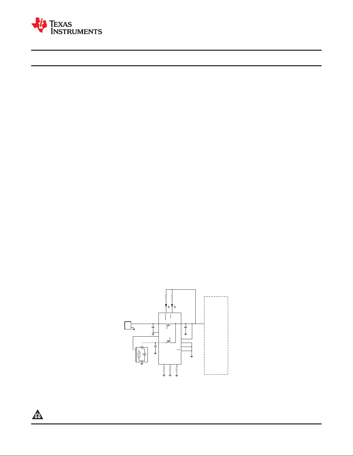
DESCRIPTION
The bq2407x series of devices are highly integrated Li-ion linear chargers and system power path management
devices targeted at space-limited portable applications. The devices operate from either a USB port or AC
adapter. The high input voltage range with input overvoltage protection supports low-cost unregulated adapters.
The bq2407x powers the system while simultaneously and independently charging the battery. This feature
reduces the number of charge and discharge cycles on the battery, allows for proper charge termination and
enables the system to run with a defective or absent battery pack. Additionally, this enables instant system
turn-on even with a totally discharged battery. The power-path management architecture also permits the battery
to supplement the system current requirements when the adapter cannot deliver the peak system currents,
enabling the use of a smaller adapter.
The battery is charged in three phases: conditioning, constant current, and constant voltage. In all charge
phases, an internal control loop monitors the IC junction temperature and reduces the charge current if the
internal temperature threshold is exceeded.
• NTC Thermistor Input
APPLICATIONS
• Smart Phones
• PDAs
• MP3 Players
• Low-Power Handheld Devices
TYPICAL APPLICATION CIRCUIT
1
Please be aware that an important notice concerning availability, standard warranty, and use in critical applications of Texas
Instruments semiconductor products and disclaimers thereto appears at the end of this data sheet.
PRODUCTION DATA information is current as of publication date.
Products conform to specifications per the terms of the Texas
Instruments standard warranty. Production processing does not
necessarily include testing of all parameters.
Copyright © 2008, Texas Instruments Incorporated
bq24072 , bq24073
bq24074 , bq24075
SLUS810 – SEPTEMBER 2008 .........................................................................................................................................................................................
These devices have limited built-in ESD protection. The leads should be shorted together or the device placed in conductive foam
during storage or handling to prevent electrostatic damage to the MOS gates.
DESCRIPTION (CONTINUED)
The charger power stage and charge current sense functions are fully integrated. The charger function has high
accuracy current and voltage regulation loops, charge status display, and charge termination. The input current
limit and charge current are programmable using external resistors.
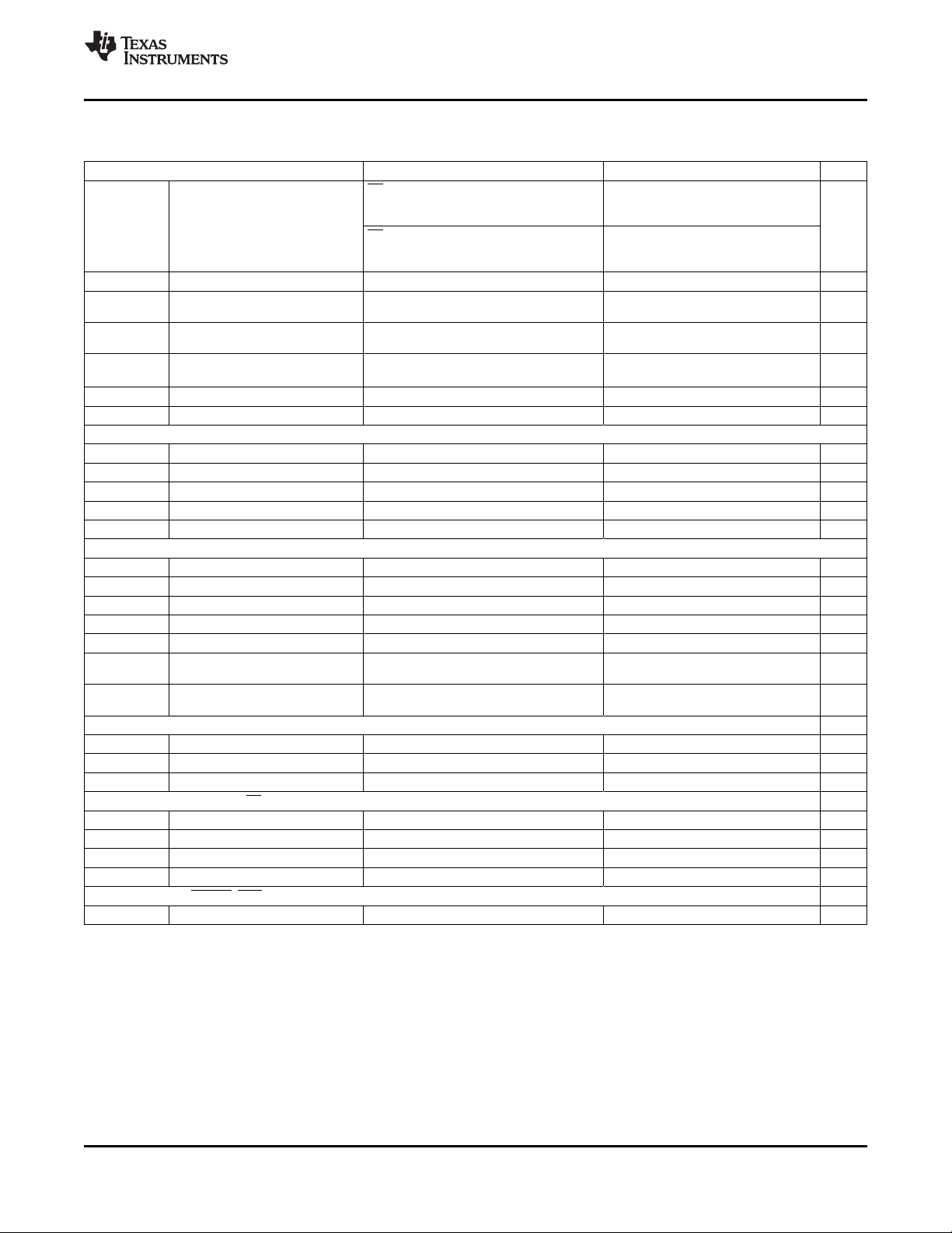
ORDERING INFORMATION
PART NUMBER V
(1) (2)
OVP
bq24072RGTR 6.6 V V
bq24072RGTT 6.6 V V
bq24073RGTR 6.6 V 4.4 V V
bq24073RGTT 6.6 V 4.4 V V
bq24074RGTR 10.5 V 4.4 V V
bq24074RGTT 10.5 V 4.4 V V
bq24075RGTR 6.6 V 5.5 V 4.3 V SYSOFF CDU
bq24075RGTT 6.6 V 5.5 V 4.3 V SYSOFF CDU
(1) The RGT package is available in the following options:
R - taped and reeled in quantities of 3,000 devices per reel.
T - taped and reeled in quantities of 250 devices per reel.
(2) This product is RoHS compatible, including a lead concentration that does not exceed 0.1% of total product weight, and is suitable for
use in specified lead-free soldering processes. In addition, this product uses package materials that do not contain halogens, including
bromine (Br) or antimony (Sb) above 0.1% of total product weight.
V
OUT(REG)
+ 200 mV V
BAT
+ 200 mV V
BAT
V
DPM
– 100 mV TD CKP
O(REG)
– 100 mV TD CKP
O(REG)
– 100 mV TD CKQ
O(REG)
– 100 mV TD CKQ
O(REG)
– 100 mV ITERM BZF
O(REG)
– 100 mV ITERM BZF
O(REG)
OPTIONAL MARKING
FUNCTION
www.ti.com
ABSOLUTE MAXIMUM RATINGS
(1)
over operating free-air temperature range (unless otherwise noted)
VALUE UNIT
IN (with respect to VSS) – 0.3 to 28 V
V
I
I
Input Voltage
I
Input Current IN 1.6 A
I
Output Current (Continuous)
O
Output Sink Current CHG, PGOOD 15 mA
T
T
Junction temperature – 40 to 150 ° C
J
Storage temperature – 65 to 150 ° C
stg
(1) Stresses beyond those listed under absolute maximum ratings may cause permanent damage to the device. These are stress ratings
only, and functional operation of the device at these or any other conditions beyond those indicated under recommended operating
conditions is not implied. Exposure to absolute-maximum-rated conditions for extended periods may affect device reliability. All voltage
values are with respect to the network ground terminal unless otherwise noted.
DISSIPATION RATINGS
PACKAGE
(2)
(1)
RGT
(1)
R
39.47 ° C/W 2.4 ° C/W 2.3 W 34.6 mW/ ° C
(1) This data is based on using the JEDEC High-K board and the exposed die pad is connected to a Cu pad on the board. The pad is
connected to the ground plane by a 2x3 via matrix.
(2) For the most current package and ordering information, see the Package Option Addendum at the end of this document, or see the TI
website at www.ti.com .
BAT (with respect to VSS) – 0.3 to 5 V
OUT, EN1, EN2, CE, TS, ISET, PGOOD, CHG, ILIM, TMR,
ITERM, SYSOFF, TD (with respect to VSS)
– 0.3 to 7 V
OUT 5 A
BAT (Discharge mode) 5 A
θ JA
R
θ JC
TA≤ 25 ° C DERATING FACTOR
POWER RATING TA> 25 ° C
2 Submit Documentation Feedback Copyright © 2008, Texas Instruments Incorporated
Product Folder Link(s): bq24072 bq24073 bq24074 bq24075
bq24072 , bq24073
bq24074 , bq24075
www.ti.com
RECOMMENDED OPERATING CONDITIONS
V
I
I
IN
I
OUT
I
BAT
I
CHG
T
J
R
ILIM
R
ISET
R
ITERM
R
TMR
ELECTRICAL CHARACTERISTICS
Over junction temperature range (0 ° ≤ TJ≤ 125 ° C) and the recommended supply voltage range (unless otherwise noted)
INPUT
UVLO Undervoltage lock-out VIN: 0 V → 4 V 3.2 3.3 3.4 V
V
hys
V
IN(DT)
V
hys
t
DGL(PGOOD)
V
OVP
V
hys
t
BLK
t
REC
ILIM, TEST ISET SHORT CIRCUIT
I
SC
V
SC
QUIESCENT CURRENT
I
BAT(PDWN)
I
IN
I
CC
POWER PATH
V
DO(IN-OUT)
V
DO(BAT-OUT)
V
O(REG)
......................................................................................................................................................................................... SLUS810 – SEPTEMBER 2008
MIN MAX UNIT
IN voltage range 4.35 26 V
IN operating voltage range V
’ 72, ’ 73, ‘ 75 4.35 6.6
‘ 74 4.35 10.5
Input current, IN pin 1.5 A
Current, OUT pin 4.5 A
Current, BAT pin (Discharging) 4.5 A
Current, BAT pin (Charging) 1.2 A
Junction Temperature – 40 125 ° C
Maximum input current programming resistor 1100 8000 Ω
Fast-charge current programming resistor 750 3000 Ω
Termination current programming resistor 0 15 k Ω
Timer programming resistor 18 72 k Ω
PARAMETER TEST CONDITIONS MIN TYP MAX UNIT
Hysteresis on UVLO VIN: 4 V → 0 V 200 300 mV
Input power detection threshold 55 80 130 mV
Hysteresis on V
IN(DT)
Deglitch time, input power detected
status
Input overvoltage protection threshold V
Input power detected when VIN> V
V
= 3.6 V, VIN: 3.5 V → 4 V
BAT
V
= 3.6 V, VIN: 4 V → 3.5 V 20 mV
BAT
Time measured from VIN: 0 V → 5 V 1 µ s
rise-time to PGOOD = LO
( ’ 72, ’ 73, ’ 75) VIN: 5 V → 7 V 6.4 6.6 6.8
( ’ 74) VIN: 5 V → 11 V 10.2 10.5 10.8
Hysteresis on OVP ( ’ 72, ’ 73, ’ 75) VIN: 7 V → 5V 110 mV
( ’ 74) VIN: 11 V → 5 V 175
Input overvoltage blanking time 50 µ s
Input overvoltage recovery time 2 ms
Time measured from VIN: 11 V → 5 V with 1 µ s
fall-time to PGOOD = LO
Current source 1.3 mA
CE = LO or HI, input power not detected, No
Sleep current into BAT pin load on OUT pin, 6.5 µ A
TJ= 85 ° C
Standby current into IN pin
Active supply current, IN pin 1.5 mA
VIN– V
OUT
V
– V
BAT
OUT
OUT pin voltage regulation (bq24072)
OUT pin voltage regulation (bq24073, VIN> V
bq24074)
OUT pin voltage regulation (bq24075) VIN> V
EN1= HI, EN2=HI, VIN= 6 V, TJ=85 ° C 50 µ A
EN1= HI, EN2=HI, VIN= 10 V, TJ=85 ° C 200
CE = LO, VIN= 6 V, no load on OUT pin,
V
> V
BAT
VIN= 4.3 V, IIN= 1A, V
I
= 1 A, VIN= 0 V, V
OUT
VIN> V
VIN> V
BAT(REG)
+ V
OUT
+ V
OUT
+ V
OUT
+ V
OUT
, (EN1, EN2) ≠ (HI, HI)
= 4.2V 300 475 mV
BAT
> 3 V 50 100 mV
BAT
, V
DO(IN-OUT)
DO(IN-OUT)
DO(IN-OUT)
DO(IN-OUT)
BAT
, V
BAT
+ V
BAT
IN(DT)
< 3.2 V 3.4
≥ 3.2 V
4.3 4.4 4.5
5.4 5.5 5.6
4 ms
520 mV
V
+
BAT
225mV
V
Copyright © 2008, Texas Instruments Incorporated Submit Documentation Feedback 3
Product Folder Link(s): bq24072 bq24073 bq24074 bq24075
bq24072 , bq24073
bq24074 , bq24075
SLUS810 – SEPTEMBER 2008 .........................................................................................................................................................................................
ELECTRICAL CHARACTERISTICS (continued)
Over junction temperature range (0 ° ≤ TJ≤ 125 ° C) and the recommended supply voltage range (unless otherwise noted)
PARAMETER TEST CONDITIONS MIN TYP MAX UNIT
EN1 = LO, EN2 = LO 90 95 100
IINmax Maximum input current EN1 = HI, EN2 = LO 450 475 500
EN2 = HI, EN1 = LO K
K
ILIM
IINmax EN2 = HI, EN1 = LO, R
V
IN(LOW)
Maximum input current factor I
Programmable input current limit
range
Input voltage threshold when input
current is reduced
≥ 500mA 1480 1550 1620 A Ω
LIM
200mA < I
< 500mA 1320 1470 1620
LIM
EN2 = LO, EN1 = X 4.35 4.5 4.63 V
Output voltage threshold when ( ’ 72, ’ 73, ’ 74) V
V
DPM
charging current is reduced 100mV
( ’ 75) 4.3 V
V
BSUP1
V
BSUP2
V
O(SC1)
Enter battery supplement mode mV
Exit battery supplement mode mV
Output short-circuit detection
threshold, power-on
Output short-circuit detection
V
O(SC2)
t
DGL(SC2)
t
REC(SC2)
threshold, supplement mode V
V
> V
OUT
indicates short-circuit
O(SC2)
Deglitch time, supplement mode short
circuit
Recovery time, supplement mode
short circuit
– 200 250 300 mV
BAT
BATTERY CHARGER
I
BAT
V
BAT
V
BAT(REG)
V
LOWV
t
DGL1(LOWV)
t
DGL2(LOWV)
I
CHG
Source current for BAT pin
short-circuit detection
BAT pin short-circuit detection
threshold
Battery charge voltage 4.16 4.20 4.24 V
Pre-charge to fast-charge transition
threshold
Deglitch time on pre-charge to
fast-charge transition
Deglitch time on fast-charge to
pre-charge transition
Battery fast charge current range 300 1200 mA
V
EN1 = LO, EN2 = HI
> V
BAT(REG)
> V
BAT
CE = LO, EN1= LO, EN2 = HI,
V
> V
Battery fast charge current K
BAT
on OUT pin, thermal loop and DPM loop not
, VIN= 5 V, IINmax > I
LOWV
active
K
ISET
I
PRECHG
K
PRECHG
Fast charge current factor 797 890 975 A Ω
Pre-charge current K
Pre-charge current factor 70 88 106 A Ω
CE = LO, (EN1, EN2) ≠ (LO, LO), A
V
> V
BAT
I
TERM
I
BIAS(ITERM)
I
TERM
Termination comparator detection
threshold (internally set)
Current for external
termination-setting resistor
Termination current threshold A
(externally set) (bq24074)
and thermal loop not active
CE = LO, (EN1, EN2) = (LO, LO),
V
BAT
and thermal loop not active
, t < t
RCH
MAXCH
> V
, t < t
RCH
MAXCH
= 8 k Ω to 1.1 k Ω 200 1500 mA
ILIM
0.8 0.9 1 V
4 7.5 11 mA
1.6 1.8 2.0 V
2.9 3 3.1 V
, VIN= 5 V CE = LO,
LOWV
, no load
CHG
, VIN= 5 V, DPM loop
, VIN= 5 V, DPM loop
0.09 × I
0.027 × I
CHG
CHG
72 75 78 µ A
K
ITERM
/R
ILIM
ILIM
O(REG)
V
≤ V
OUT
BAT
– 40
V
OUT
V
– 20
BAT
250 µ s
60 ms
25 ms
25 ms
/R
ISET
ISET
/R
PRECHG
ISET
0.1 × I
CHG
0.033 × I
CHG
× R
/ R
ITERM
–
≥
ISET
0.11 × I
0.040 × I
www.ti.com
mA
A
V
A
A
CHG
CHG
4 Submit Documentation Feedback Copyright © 2008, Texas Instruments Incorporated
Product Folder Link(s): bq24072 bq24073 bq24074 bq24075
bq24072 , bq24073
bq24074 , bq24075
www.ti.com
ELECTRICAL CHARACTERISTICS (continued)
Over junction temperature range (0 ° ≤ TJ≤ 125 ° C) and the recommended supply voltage range (unless otherwise noted)
K
ITERM
t
DGL(TERM)
V
RCH
t
DGL(RCH)
t
DGL(NO-IN)
I
BAT(DET)
t
DET
BATTERY CHARGING TIMERS
t
PRECHG
t
MAXCHG
t
PRECHG
t
MAXCHG
K
TMR
BATTERY-PACK NTC MONITOR
I
NTC
V
HOT
V
HYS(HOT)
V
COLD
V
HYS(COLD)
t
DGL(TS)
V
DIS(TS)
THERMAL REGULATION
T
J(REG)
T
J(OFF)
T
J(OFF-HYS)
LOGIC LEVELS ON EN1, EN2, CE, SYSOFF, TD
V
IL
V
IH
I
IL
I
IH
LOGIC LEVELS ON PGOOD, CHG
V
OL
(1) These numbers set trip points of 0 ° C and 50 ° C while charging, with 3 ° C hysteresis on the trip points, with a Vishay Type 2 curve NTC
......................................................................................................................................................................................... SLUS810 – SEPTEMBER 2008
PARAMETER TEST CONDITIONS MIN TYP MAX UNIT
CE = LO, (EN1, EN2) ≠ (LO, LO), A
0.008 0.0100 0.012
0.0225 0.0300 0.0375
K Factor for termination detection
threshold (externally set) (bq24074)
V
> V
BAT
and thermal loop not active
, t < t
RCH
MAXCH
CE = LO, (EN1, EN2) = (LO, LO),
V
> V
BAT
and thermal loop not active
, t < t
RCH
MAXCH
, VIN= 5 V, DPM loop
, VIN= 5 V, DPM loop
Deglitch time, termination detected 0 25 ms
V
Recharge detection threshold mV
BAT(REG)
– 140 – 100 – 60
V
BAT(REG)
Deglitch time, recharge threshold
detected
V
Delay time, input power loss to
charger turn-off
= 3.6 V. Time measured from
BAT
VIN: 5 V → 3 V 1 µ s fall-time
Sink current for battery detection 5 7.5 10 mA
Battery detection timer 250 ms
Pre-charge safety timer value TMR = floating 1440 1800 2160 s
Charge safety timer value TMR = floating 14400 18000 21600 s
Pre-charge safety timer value 18 k Ω < R
Charge safety timer value 18 k Ω < R
< 72 k Ω R
TMR
< 72 k Ω 10 × RTMR × K
TMR
× K
TMR
Timer factor 36 48 60 s/k Ω
(1)
NTC bias current 72 75 78 µ A
High temperature trip point Battery charging 270 300 330 mV
Hysteresis on high trip point Battery charging 30 mV
Low temperature trip point Battery charging 2000 2100 2200 mV
Hysteresis on low trip point Battery charging 300 mV
Deglitch time, pack temperature fault
detection
TS function disable threshold
(bq24072, bq24073)
Battery charging 50 ms
VIN- 200mV V
Temperature regulation limit 125 ° C
Thermal shutdown temperature 155 ° C
Thermal shutdown hysteresis 20 ° C
Logic LOW input voltage 0 0.4 V
Logic HIGH input voltage 1.4 6 V
VIL= 0V 1 µ A
VIH= 1.4V 10 µ A
Output LOW voltage I
= 5 mA 0.4 V
SINK
with an R25 of 10 k Ω .
V
BAT(REG)
62.5 ms
20 ms
TMR
TMR
s
s
Copyright © 2008, Texas Instruments Incorporated Submit Documentation Feedback 5
Product Folder Link(s): bq24072 bq24073 bq24074 bq24075
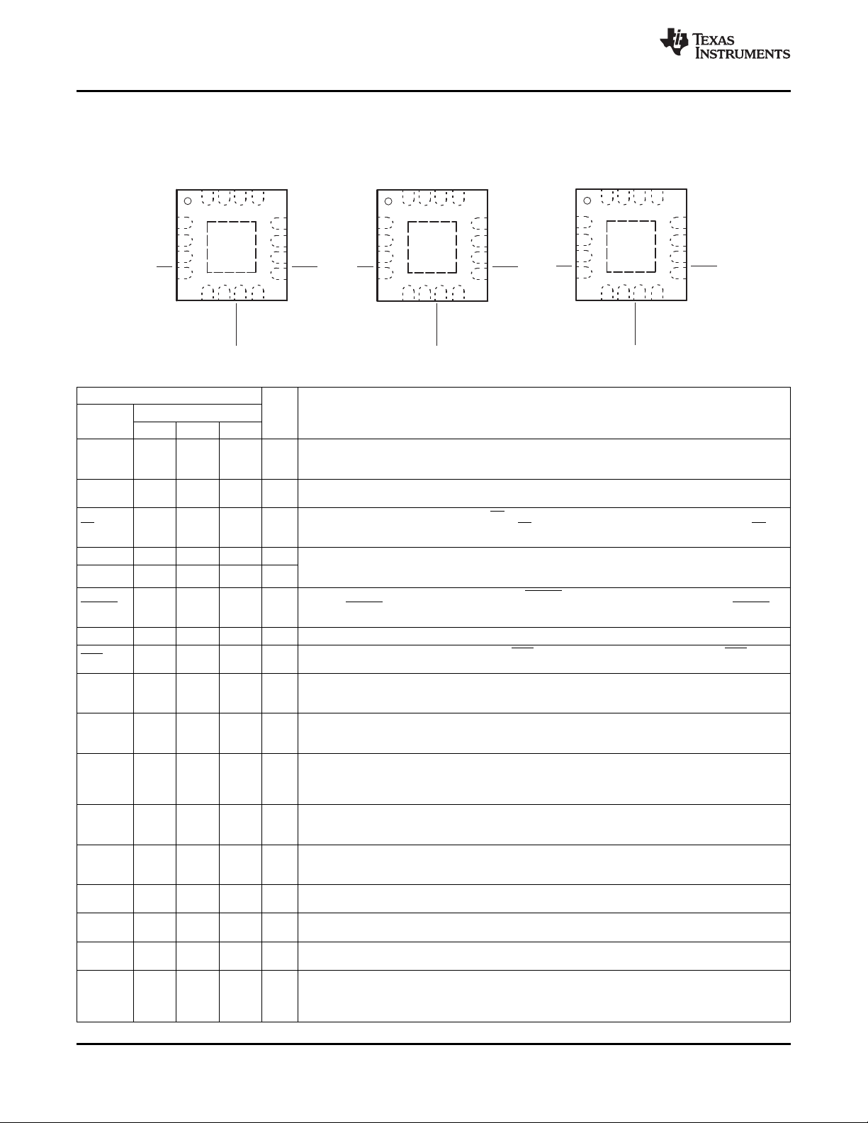
1
2
3
4
12
11
10
9
ILIM
OUT
OUT
CHG
TS
BAT
BAT
CE
ISET
TD
PGOOD
VSS
TMR
IN
EN2
EN1
16 15 14 13
5 6 7 8
bq24075
1
2
3
4
12
11
10
9
ILIM
OUT
OUT
CHG
TS
BAT
BAT
CE
ISET
ITERM
PGOOD
VSS
TMR
IN
EN2
EN1
16 15 14 13
5 6 7 8
bq24074
SYSOFF
1
2
3
4
12
11
10
9
ILIM
OUT
OUT
CHG
TS
BAT
BAT
CE
ISET
PGOOD
VSS
TMR
IN
EN2
EN1
16 15 14 13
5 6 7 8
bq24072
bq24073
bq24072 , bq24073
bq24074 , bq24075
SLUS810 – SEPTEMBER 2008 .........................................................................................................................................................................................
RGT PACKAGE
(Top View)
TERMINAL FUNCTIONS
TERMINAL
NAME
TS 1 1 1 I a 10k Ω NTC thermistor.To disable the external temperature sense circuitry, connect a 10k Ω resistor from TS
BAT 2, 3 2, 3 2, 3 I/O
CE 4 4 4 I mode. In standby mode, OUT is active. Connect CE to a low logic level to enable the battery charger. CE is
EN2 5 5 5 I Input Current Limit Configuration Inputs. Use EN1 and EN2 control the maximum input current and enable
EN1 6 6 6 I
PGOOD 7 7 7 O detected. PGOOD is high-impedance when the input power is not within specified limits. Connect PGOOD to
VSS 8 8 8 – Ground. Connect to the thermal pad and to the ground rail of the circuit.
CHG 9 9 9 O
OUT 10, 11 10, 11 10, 11 O above the regulation voltage. Connect OUT to the system load. Bypass OUT to VSS with a 4.7 µ F to 47 µ F
ILIM 12 12 12 I the maximum input current (EN2=1, EN1=0). The input current includes the system load and the battery
IN 13 13 13 I
TMR 14 14 14 I to disable all timers. Connect a 18 k Ω to 72 k Ω resistor between TMR and VSS to program the timers a
TD 15 – – I charger termination. See the TD section in this datasheet for a description of the behavior when termination is
ITERM – 15 – I
SYSOFF – – 15 I
ISET 16 16 16 I/O
Thermal The thermal pad must be connected to the same potential as the VSS pin on the printed circuit board. Do not
Pad use the thermal pad as the primary ground input for the device. VSS pin must be connected to ground at all
6 Submit Documentation Feedback Copyright © 2008, Texas Instruments Incorporated
' 72, ' 73 ' 74 ' 75
NO. I/O DESCRIPTION
External NTC Thermistor Input. Connect the TS input to the NTC thermistor in the battery pack. TS moniitors
to VSS.
Charger Power Stage Output and Battery Voltage Sense Input. Connect BAT to the positive terminal of the
battery. Bypass BAT to VSS with a 4.7 µ F to 47 µ F ceramic capacitor.
Charge Enable Active-Low Input. Connect CE to a high logic level to place the battery charger in standby
internally pulled down with ~285 k Ω .
USB compliance. See Table 2 for the description of the operation states. EN1 and EN2 are internally pulled
down with ~285 k Ω .
Open-drain Power Good Status Indication Output. PGOOD pulls to VSS when a valid input source is
the desired logic voltage rail using a 10k Ω -100k Ω resistor.
Open-Drain Charging Status Indication Output. CHG pulls to VSS when the battery is charging. CHG is high
impedance when charging is complete and when charger is disabled.
System Supply Output. OUT provides a regulated output when the input is below the OVP threshold and
ceramic capacitor.
Adjustable Current Limit Programming Input. Connect a 1100 Ω to 8 k Ω resistor from ILIM to VSS to program
charge current.
Input Power Connection. Connect IN to the connected to external DC supply (AC adapter or USB port). The
input operating range is 4.35V to 6.6V (bq24072, bq24073, and bq24075) or 4.35V to 10.5V (bq23074). The
input can accept voltages up to 26V without damage but operation is suspended. Connect bypass capacitor 1
µ F to 10 µ F to VSS.
Timer Programming Input. TMR controls the pre-charge and fast-charge safety timers. Connect TMR to VSS
desired length. Leave TMR unconnected to set the timers to the default values.
Termination Enable Input. Connect TD to VSS to enable charger termination. Connect TD high to disable
disabled. TD is internally pulled down to VSS with ~285 k Ω .
Termination Current Programming Input. Connect a 0 Ω to 15 k Ω resistor from ITERM to VSS to program the
termination current. Leave ITERM unconnected to set the termination current to the internal default value.
System Enable Input. Connect SYSOFF high to disconnect OUT from the input power when . Internally pulled
–
up to V
Fast Charge Current Programming Input. Connect a 750 Ω to 3 k Ω resistor from ISET to VSS to program the
fast charge current level.
There is an internal electrical connection between the exposed thermal pad and the VSS pin of the device.
times.
through a large resistor (~5 M Ω ).
BAT
Product Folder Link(s): bq24072 bq24073 bq24074 bq24075
www.ti.com
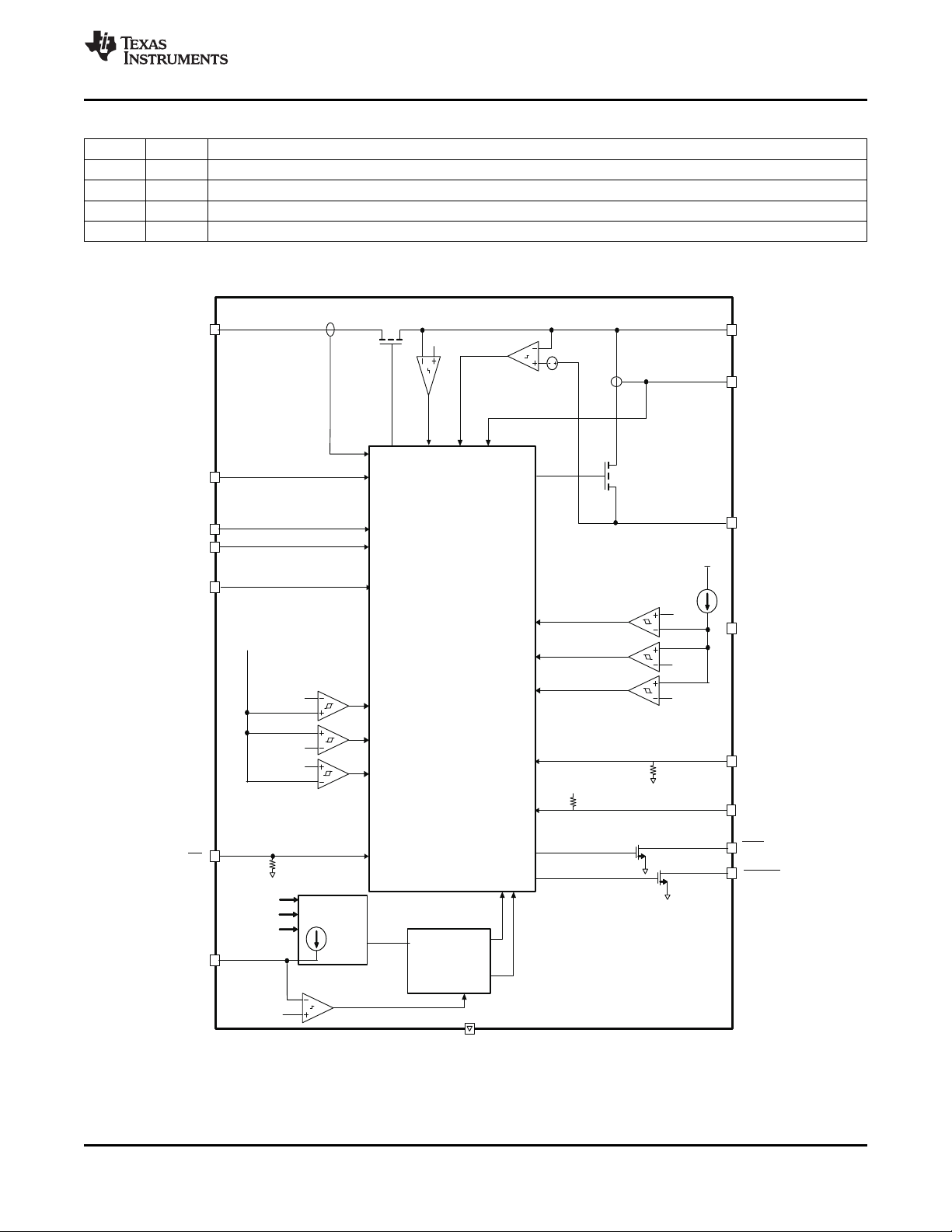
Q1
Q2
I
NTC
V
HOT
V
COLD
V
UVLO
V
OVP
Dynamically
Controlled
Oscillator
V
IPRECHG
V
ICHG
V
ISET
-100mV
CE
IN
EN1
EN2
PGOOD
TS
OUT
BAT
ISET
ILIM
TMR
OUT-SC2
Timersdisabled
SYSOFF
('75)
ITERM
('74)
V
BAT
250mV
FAST-CHARGE
and
PRE-CHARGE
TIMERS
VSS
CHARGE ANDDYNAMIC
POWERPATH
MANAGEMENT CONTROL
V
IN
V +V
BAT IN-DT
CHG
V
DIS(TS)
TD
('72,'73)
V
O(SCI)
OUT-SC1
www.ti.com
......................................................................................................................................................................................... SLUS810 – SEPTEMBER 2008
EN2 EN1 Maximum input current into IN pin
0 0 100 mA. USB100 mode
0 1 500 mA. USB500 mode
1 0 Set by an external resistor from ILIM to VSS
1 1 Standby (USB suspend mode)
SIMPLIFIED BLOCK DIAGRAM
bq24072 , bq24073
bq24074 , bq24075
Table 1. EN1/EN2 Settings
Copyright © 2008, Texas Instruments Incorporated Submit Documentation Feedback 7
Product Folder Link(s): bq24072 bq24073 bq24074 bq24075
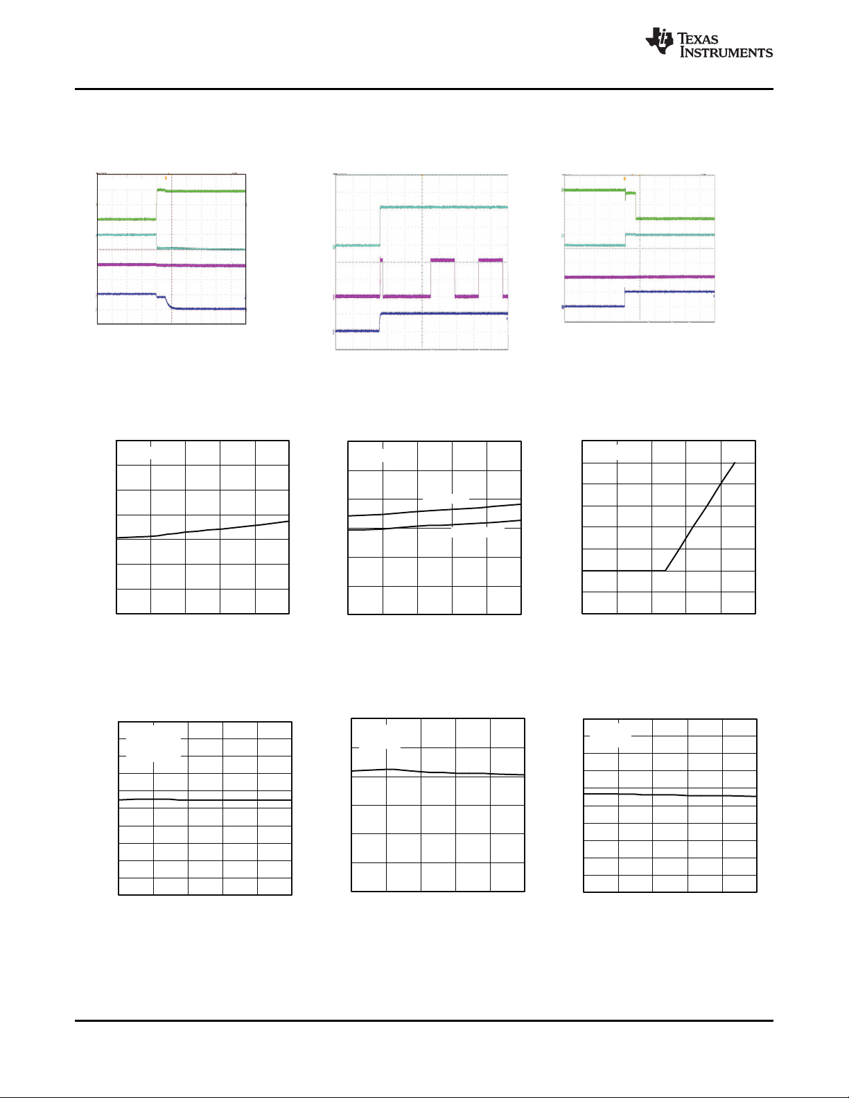
I
BAT
V
OUT
V
4V
BAT
V
IN
2V/div
500mV/div
100mA/div
-200mA
ChargingBattery
40ms/div
5V/div
40ms/div
I
BAT
V
4.4V
OUT
V
4V
BAT
V
IN
2V/div
5V
0V
500mV/div
200mA
BatterySupplying
Load
-200mA
ChargingBattery
R =6.6
OUT
W
V
OUT
V
BAT
V
IN
2V/div
200ms/div
2V/div
5V/div
0
20
40
60
80
100
120
0
25
50 75 100
125
T -JunctionTemperature-°C
J
DropoutVoltage-V -V
BAT OUT
VBAT =3V
VBAT =3.9V
I =1 A
L
3
3.2
3.4
3.6
3.8
4
4.2
4.4
4.6
2
2.5
3
3.5 4
4.5
V -OutputVoltage-V
O
V -BatteryVoltage-V
BAT
V =5V
IN
0
0.1
0.2
0.3
0.4
0.5
0.6
0.7
0 25
50 75
100
125
T -JunctionTemperature-°C
J
DropoutVoltage-V -V
IN OUT
I =1 A
L
5.25
5.30
5.35
5.40
5.45
5.50
5.55
5.60
5.65
5.70
5.75
0 25 50 75 100 125
T -JunctionTemperature-°C
J
V -OutputVoltage-V
O
V =6V,
I =1 A
IN
L
4.30
4.33
4.35
4.38
4.40
4.43
4.45
0
25
50 75 100 125
T -JunctionTemperature-°C
J
V -OutputVoltage-V
O
V =5V,
I =1 A
IN
L
3.60
3.62
3.64
3.66
3.68
3.70
3.72
3.74
3.76
3.78
3.80
0 25 50 75 100 125
T -JunctionTemperature-°C
J
V -OutputVoltage-V
O
V =5V,
V =3.5V,
I =1 A
IN
BAT
L
bq24072 , bq24073
bq24074 , bq24075
SLUS810 – SEPTEMBER 2008 .........................................................................................................................................................................................
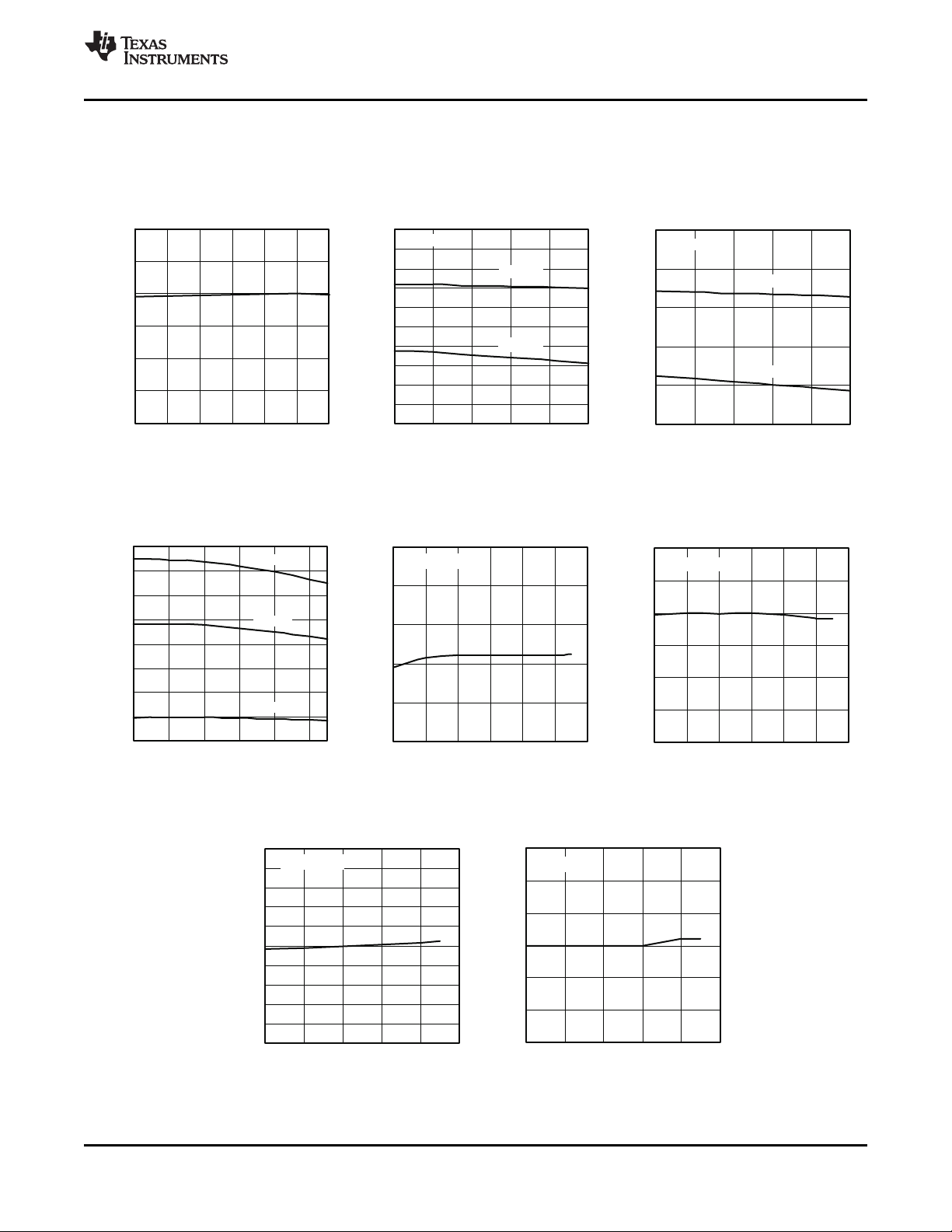
TYPICAL CHARACTERISTICS
ADAPTER REMOVAL
BATTERY CONNECTED ADAPTER HOT-PLUG ADAPTER HOT-PLUG
R
= 6.6 Ω NO BATTERY CONNECTED BATTERY CONNECTED
OUT
Figure 1. Figure 2. Figure 3.
www.ti.com
DROPOUT VOLTAGE vs OUTPUT REGULATION VOLTAGE
DROPOUT VOLTAGE bq24072
vs TEMPERATURE vs
TEMPERATURE NO INPUT SUPPLY BATTERY VOLTAGE
Figure 4. Figure 5. Figure 6.
bq24072 bq24073/ 74 bq24075
OUTPUT REGULATION VOLTAGE OUTPUT REGULATION VOLTAGE OUTPUT REGULATION VOLTAGE
vs vs vs
TEMPERATURE TEMPERATURE TEMPERATURE
8 Submit Documentation Feedback Copyright © 2008, Texas Instruments Incorporated
Figure 7. Figure 8. Figure 9.
Product Folder Link(s): bq24072 bq24073 bq24074 bq24075
10.20
10.25
10.30
10.35
10.40
10.45
10.50
10.55
10.60
10.65
10.70
0
25
50
75
100
125
T -JunctionTemperature-°C
J
V -OutputVoltageThreshold-V
OVP
V Rising
I
V Falling
I
10.5V
6.45
6.50
6.55
6.60
6.65
6.70
0 25 50 75 100 125
T -JunctionTemperature-°C
J
V -OutputVoltageThreshold-V
OVP
6.6V
V Rising
I
V Falling
I
4.180
4.185
4.190
4.195
4.200
4.205
4.210
0
5
10 15 20
25
30
T -JunctionTemperature-°C
J
V -RegulationVoltage-V
BA
T
0
100
200
300
400
500
600
700
800
5 6 7 8 9 10
V -InputVoltage-V
I
I -InputCurrent-mA
LIM
RILIM
USB500
USB100
R=900
ISET
W
0.95
0.97
0.99
1.01
1.03
1.05
3
3.2
3.4
3.6
3.8
4 4.2
I -FastChargeCurrent- A
BAT
V -BatteryVoltage-V
BAT
R=3k
ISET
W
280
285
290
295
300
305
310
3 3.2 3.4 3.6 3.8 4 4.2
I -FastChargeCurrent- A
BAT
V -BatteryVoltage-V
BAT
28.5
29
29.5
30
30.5
31
31.5
2 2.2 2.4 2.6 2.8 3
I -PrechargeCurrent- A
BAT
V -BatteryVoltage-V
BAT
R=3k
ISET
W
95
96
97
98
99
100
101
102
103
104
105
2 2.2 2.4 2.6 2.8 3
I -PrechargeCurrent- A
BAT
V -BatteryVoltage-V
BAT
R=900
ISET
W
bq24072 , bq24073
bq24074 , bq24075
www.ti.com
......................................................................................................................................................................................... SLUS810 – SEPTEMBER 2008
TYPICAL CHARACTERISTICS (continued)
bq24072/ 73/ 75 bq24074
OVERVOLTAGE PROTECTION OVERVOLTAGE PROTECTION
BAT REGULATION VOLTAGE THRESHOLD THRESHOLD
vs vs vs
TEMPERATURE TEMPERATURE TEMPERATURE
Figure 10. Figure 11. Figure 12.
bq24072/ 73/ 75 bq24074
INPUT CURRENT LIMIT INPUT CURRENT LIMIT FASTCHARGE CURRENT
vs vs vs
INPUT VOLTAGE INPUT VOLTAGE BATTERY VOLTAGE
Copyright © 2008, Texas Instruments Incorporated Submit Documentation Feedback 9
Figure 13. Figure 14. Figure 15.
FASTCHARGE CURRENT PRECHARGE CURRENT
vs vs
BATTERY VOLTAGE BATTERY VOLTAGE
Figure 16. Figure 17.
Product Folder Link(s): bq24072 bq24073 bq24074 bq24075
V
OVP
V -V
OVP hys(OVP)
V +V
BAT IN(DT)
V +V -V
BAT IN(DT) hys(INDT)
UVLO
UVLO -V
hys(UVLO)
PGOOD
t
DGL(PGOOD)
t
DGL(OVP)
t
DGL(PGOOD)
t
DGL(NO-IN)
V
IN
t<t
DGL(OVP)
TypicalInputVoltage
OperatingRange
V
BAT
V
LOWV
I
CHG
I
PRE-CHG
Pre-Charge
Fast-Charge
Pre-Charge
Fast-Charge
t<t
DGL1(LOWV)
t
DGL1(LOWV)
t
DGL2(LOWV)
t<t
DGL2(LOWV)
t
DGL1(LOWV)
V
RCH
V
BAT
t<t
DGL(RCH)
t
DGL(RCH)
Re-Charge
bq24072 , bq24073
bq24074 , bq24075
SLUS810 – SEPTEMBER 2008 .........................................................................................................................................................................................
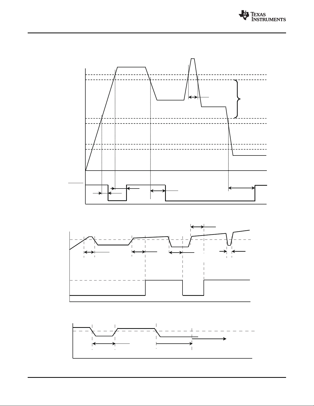
EXPLANATION OF DEGLITCH TIMES AND COMPARATOR HYSTERESIS
Figures not to scale
www.ti.com
10 Submit Documentation Feedback Copyright © 2008, Texas Instruments Incorporated
Figure 18. Power-Up, Power-Down
Figure 19. Pre- to Fast-Charge, Fast- to Pre-Charge Transition – t
Product Folder Link(s): bq24072 bq24073 bq24074 bq24075
Figure 20. Recharge – t
DGL(RCH)
DGL1(LOWV)
, t
DGL2(LOWV)
Turn
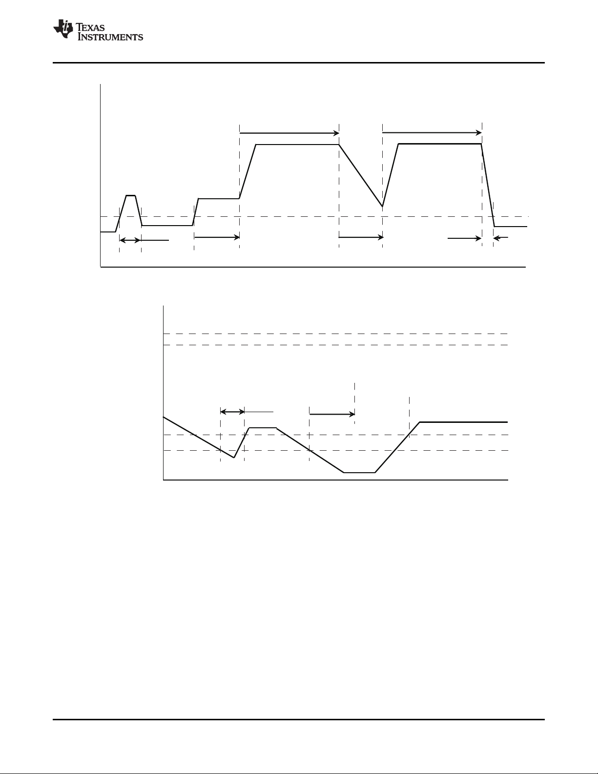
Q2OFF
t
REC(SC2)
Force
Q2ON
Turn
Q2OFF
t
REC(SC2)
Force
Q2ON
V -V
BAT OUT
V
O(SC2)
Recover
t<t
DGL(SC2)
t
DGL(SC2)
t
DGL(SC2)
t<t
DGL(SC2)
V
COLD
V -V
COLD hys(COLD)
V -V
HOT hys(HOT)
V
HOT
V
TS
t<t
DGL(TS)
t
DGL(TS)
Suspend
Charging
Resume
Charging
bq24072 , bq24073
bq24074 , bq24075
www.ti.com
......................................................................................................................................................................................... SLUS810 – SEPTEMBER 2008
Figure 21. OUT Short-Circuit – Supplement Mode
DETAILED FUNCTIONAL DESCRIPTION
The bq2407x devices are integrated Li-Ion linear chargers and system power path management devices targeted
at space-limited portable applications. The device powers the system while simultaneously and independently
charging the battery. This feature reduces the number of charge and discharge cycles on the battery, allows for
proper charge termination and enables the system to run with a defective or absent battery pack. It also allows
instant system turn-on even with a totally discharged battery. The input power source for charging the battery
and running the system can be an AC adapter or a USB port. The devices feature Dynamic Power Management,
which shares the source current between the system and battery charging, and automatically reduces the
charging current if the system load increases. Additionally, when charging from a USB port, the device reduces
the input current if the input voltage falls below a threshold, preventing the USB port from crashing. The
power-path architecture also permits the battery to supplement the system current requirements when the
adapter cannot deliver the peak system currents. The startup state diagram is shown in Figure 23 .
Copyright © 2008, Texas Instruments Incorporated Submit Documentation Feedback 11
Figure 22. Battery Pack Temperature Sensing – TS Pin. Battery Temperature Increasing
Product Folder Link(s): bq24072 bq24073 bq24074 bq24075

AnyState
IfVIN<V
UVLO
,
gotoPowerDown
PowerDown
AllIC functionsOFF
/PGOOD=Hi-Z
/CHG=Hi-Z
Q2=ON
VIN>V
UVLO
No
Yes
Sleep
/PGOOD=Hi-Z
/CHG=Hi-Z
Q2=ON
VIN>V
BAT
No
Yes
Standby
/CHG=Hi-Z
Q2=ON
VIN<V
OVP
Yes
No
USBSuspend
Yes
No
BeginStartupChecks
Goto
BeginCharge
AnyState
IfVIN>V
OVP
,
gotoStandby
AnyState
IfUSBSuspend,
gotoStandby
ILIMshort
Yes
No
ISET short
Yes
No
V
OUT
<V
O(SC)
?
Yes
No
Idle
Q2=OFF
/CE= Low
Yes
No
TurnonQ1
@100mA
AnyState
IfV
OUT
<V
O(SC)
,
gotoBeganStartup
Check
/PGOOD=Hi-Z
/PGOOD=Low
TurnonQ1
@(EN1,EN2)
TD=High
No
Yes
Goto
TerminationDisable
AnyState
IfVIN<V
BAT
,
gotoPowerDown
bq24072 , bq24073
bq24074 , bq24075
SLUS810 – SEPTEMBER 2008 .........................................................................................................................................................................................
www.ti.com
Figure 23. Startup State Diagram
UNDER-VOLTAGE LOCKOUT (UVLO)
The bq2407X family remains in power down mode when the input voltage at the IN pin is below the undervoltage
threshold (UVLO).
During the power down mode the host commands at the control inputs ( CE, EN1 and EN2) are ignored. The Q1
FET connected between IN and OUT pins is off, and the status outputs CHG and PGOOD are high impedance.
The Q2 FET that connects BAT to OUT is ON. (If SYSOFF is high, Q2 is off). During power down mode, the
V
OUT(SC2)
12 Submit Documentation Feedback Copyright © 2008, Texas Instruments Incorporated
circuitry is active and monitors for overload conditions on OUT.
Product Folder Link(s): bq24072 bq24073 bq24074 bq24075

bq24072 , bq24073
bq24074 , bq24075
www.ti.com
POWER ON
When V
commands at the control inputs ( CE, EN1 and EN2) are ignored. The Q1 FET connected between IN and OUT
pins is off, and the status outputs CHG and PGOOD are high impedance. The Q2 FET that connects BAT to
OUT is ON. (If SYSOFF is high, Q2 is off). During this mode, the V
overload conditions on OUT.
Onve V
and EN2 inputs are read. The device enters standby mode if (EN1 = EN2 = HI) or if an input overvoltage
condition occurs. In standby mode, Q1 is OFF and Q2 is ON so OUT is connected to the battery input. (If
SYSOFF is high, FET Q2 is off). During this mode, the V
conditions on OUT.
When the input voltage at IN is within the valid range: V
the EN1 and EN2 pins indicate that the USB suspend mode is not enabled [(EN1, EN2) ≠ (HI, HI)] all internal
timers and other circuit blocks are activated. The device then checks for short-circuits at the ISET and ILIM pins.
If no short conditions exists, the device switches on the input FET Q1 with a 100mA current limit to checks for a
short circuit at OUT. If V
and R
input source (Q1 is on), and the device continuously monitors the status of CE, EN1 and EN2 as well as the
input voltage conditions. Q2 is turned on to charge the battery and whenever the input source cannot deliver the
required load current (supplement mode).
......................................................................................................................................................................................... SLUS810 – SEPTEMBER 2008
exceeds the UVLO threshold, the bq2407x powers up. While V
IN
OUT(SC2)
rises above V
IN
and the device enters into the normal operation. During normal operation, the system is powered by the
ILIM
+ V
BAT
rises above V
OUT
, PGOOD is driven low to indicate the valid power status and the CE, EN1,
IN(DT)
OUT(SC2)
> UVLO AND V
IN
, the FET Q1 switches to the current limit threshold set by EN1, EN2
SC
circuitry is active and monitors for overload
is below V
IN
+ V
BAT
circuitry is active and monitors for
> V
IN
+ V
BAT
AND V
IN(DT)
, the host
IN(DT)
< V
IN
, and
OVP
POWER-PATH MANAGEMENT
The bq2407x features an OUT output that powers the external load connected to the battery. This output is
active whenever a source is connected to IN or BAT. The following sections discuss the behavior of OUT with a
source connected to IN to charge the battery and a battery source only.
IN SOURCE CONNECTED
With a source connected, the power-path management circuitry of the bq2407x monitors the input current
continuously. The OUT output for the bq24073/ 74/ 75 is regulated to a fixed voltage (V
the OUT output is regulated to 200mV above the voltage at BAT. When the BAT voltage falls below 3.2V, OUT is
clamped to 3.4V. Therefore, the minimum voltage at OUT with an adapter connected is 3.4V, allowing for proper
startup of the system load. The current into IN is shared between charging the battery and powering the system
load at OUT. The bq2407x has internal selectable current limits of 100mA (USB100) and 500mA (500mA) for
charging from USB ports, as well as a resistor-programmable input current limit. The power path utilizes
additional feature for operation from current-limited USB ports. When EN1 and EN2 are configured for USB100
(EN2=0, EN1=0) or USB500 (EN2=0, EN2=1) modes, the input voltage is monitored. If V
input current limit is reduced to prevent the input voltage from falling further.
The input current limit selection is controlled by the state of the EN1 and EN2 pins as shown in Table 1 . When
using the resistor-programmable current limit, the input current limit is set by the value of the resistor connected
from the ILIM pin to VSS, and is given by the equation:
I
= K
IN-MAX
/R
ILIM
ILIM
The input current limit is adjustable up to 1.5A. The valid resistor range is 1.1 k Ω to 8 k Ω .
When the IN source is connected, priority is given to the system load. The DPM and Battery Supplement modes
are used to maintain the system load. Figure 24 and Figure 25 illustrate examples of the DPM and supplement
modes. These modes are explained in detail in the following sections.
). For the bq24072,
O(REG)
IN
falls to V
, the
IN-LOW
DPM Mode
When the sum of the charging and system load currents exceeds the preset maximum input current
(programmed with EN1, EN2 and ILIM pins), the voltage at OUT decreases. Once the voltage on the OUT pin
falls to V
, the bq2407x enters DPM mode. In this mode, the charging current is reduced as the OUT current
DPM
goes up in order to maintain the system output.
Copyright © 2008, Texas Instruments Incorporated Submit Documentation Feedback 13
Product Folder Link(s): bq24072 bq24073 bq24074 bq24075

A
1200mA
900mA
400mA
0mA
I
OUT
900mA
500mA
0mA
I
IN
500mA
-300mA
0mA
I
BAT
3.8V
3.7V
~3.6V
V
OUT
DPMLoop Active
SupplementMode
bq24072 , bq24073
bq24074 , bq24075
SLUS810 – SEPTEMBER 2008 .........................................................................................................................................................................................
Battery Supplement Mode
While in DPM mode, if the charging current falls to zero and the system load current increases beyond the
programmed input current limit, the voltage at OUT reduces further. When the OUT voltage drops below the
V
when the voltage at OUT rises above the V
threshold, the battery supplements the system load. The battery stops supplementing the system load
BSUP1
threshold.
BSUP2
During supplement mode, the battery supplement current is not regulated, however there is a short circuit
protection circuit built in. If during battery supplement mode, the voltage at OUT drops 250mV below the BAT
voltage, the OUT output is turned off if the overload exists after t
DGL(SC2)
and the device enters Power-On Reset
Mode
www.ti.com
Figure 24. bq24072 DPM and Battery Supplement Modes (V
= V
OREG
BAT
+ 200mV, V
= 3.6V)
BAT
14 Submit Documentation Feedback Copyright © 2008, Texas Instruments Incorporated
Product Folder Link(s): bq24072 bq24073 bq24074 bq24075

A
1200mA
900mA
400mA
0mA
I
OU
T
900mA
500mA
0mA
I
IN
500mA
-300mA
0mA
I
BA
T
4.4V
4.3V
~3.6V
V
OU
T
DPMLoop Active
SupplementMode
bq24072 , bq24073
bq24074 , bq24075
www.ti.com
......................................................................................................................................................................................... SLUS810 – SEPTEMBER 2008
Figure 25. bq24073 DPM and Battery Supplement Modes (V
IN SOURCE NOT CONNECTED
When no source is connected to the IN input, OUT is powered strictly from the battery. During this mode the
current into OUT is not regulated, similar to Battery Supplement Mode, however the short circuit circuitry is
active. If the OUT voltage falls below the BAT voltage by 250mV for longer than t
short circuit recovery timer then starts counting. After t
REC(SC2)
, OUT turns on and attempts to restart. If the short
circuit remains, OUT is turned off and the counter restarts. This ON/OFF cycle continues until the overload
condition is removed.
=4.4V, V
OREG
DGL(SC2)
= 3.6V)
BAT
, OUT is turned off. The
BATTERY CHARGING
Dive CE low after IC startup to initiate battery charging. First, the device checks for a short-circuit on the BAT pin
by sourcing I
BAT(SC)
battery charging continues. The battery is charged in three phases: conditioning pre-charge, constant current fast
charge (current regulation) and a constant voltage tapering (voltage regulation). In all charge phases, an internal
control loop monitors the IC junction temperature and reduces the charge current if an internal temperature
threshold is exceeded.
Figure 26 illustrates a normal Li-Ion charge cycle using the bq2407x:
to the battery and monitoring the voltage. When the BAT voltage exceeds V
BAT(SC)
, the
Copyright © 2008, Texas Instruments Incorporated Submit Documentation Feedback 15
Product Folder Link(s): bq24072 bq24073 bq24074 bq24075

PRECHARGE CCFASTCHARGE CVTAPER DONE
BatteryVoltage
BatteryCurrent
CHG=Hi-z
V
BAT(REG)
I
O(CHG)
V
LOWV
I
(PRECHG)
I
(TERM)
bq24072 , bq24073
bq24074 , bq24075
SLUS810 – SEPTEMBER 2008 .........................................................................................................................................................................................
www.ti.com
Figure 26. Typical Charge Cycle
In the pre-charge phase, the battery is charged at with the pre-charge current (I
crosses the V
reaches V
BAT(REG)
battery approaches full charge. When the battery current reaches I
threshold, the battery is charged with the fast-charge current (I
LOWV
, the battery is held at a constant voltage of V
BAT(REG)
TERM
and the charge current tapers off as the
, the CHG pin indicates charging done by
PRECHG
). Once the battery voltage
). As the battery voltage
CHG
going high-impedance.
Note that termination detection is disabled whenever the charge rate is reduced from the set point because of the
actions of the thermal loop, the DPM loop or the V
loop.
IN(LOW)
The value of the fast-charge current is set by the resistor connected from the ISET pin to VSS, and is given by
the equation
I
= K
CHG
The charge current limit is adjustable up to 1.2A. The valid resistor range is 750 Ω to 3 k Ω . Note that if I
programmed as greater than the input current limit, the battery will not charge at the rate of I
/R
ISET
ISET
, but at the
CHG
slower rate of IINmax (minus the load current on the OUT pin, if any). In this case, the charger timers will be
proportionately slowed down. Figure 27 illustrates the battery charger state diagram.
is
CHG
16 Submit Documentation Feedback Copyright © 2008, Texas Instruments Incorporated
Product Folder Link(s): bq24072 bq24073 bq24074 bq24075

BeginCharge
V
BAT
>V
BAT(SC)
No
Yes
GotoFault
TurnonI
BAT(SC)
TurnoffI
BAT(SC)
Resett
PRECHG
/CHG=Low
Pre-Charge
Enablet
PRECHG
EnableI
PRECHG
V
BAT
>V
LOWV
No
Yes
t
PRECHG
timeout
No
Yes
TSHot,Cold
Yes
Turnoffcharger
Halt t
PRECHG
GotoFault
DisableI
PRECHG
Resett
MAXCHG
CC/CVCharge
Enablet
MAXCHG
EnableI
CHG
I
BAT
<I
TERM
No
Yes
t
MAXCHG
timeout
Yes
TSHot,Cold
Yes
Turnoffcharger
Halt t
MAX CHG
No
No
Turnoffcharger
/CHG=Hi-Z
Goto
Re-Charge
AnyState
IfVIN<V
UVLO
,
gotoPowerDown
AnyState
IfVIN>V
OVP
,
gotoStandby
AnyState
If /CE=High,
gotoIdle
AnyState
IfV
BAT
<V
BAT(SC)
,
gotoBeginCharge
AnyState
IfV
OUT
<V
O(SC)
,
gotoBegin
StartupChecks
AnyState
IfUSBSuspend,
gotoStandby
AnyState
IfVIN<V
BAT
,
gotoPowerDown
TJ> T
J(OFF)
Yes
Turnoffcharger
Halt t
PRECHG
No
No
TJ> T
J(OFF)
Yes
Turnoffcharger
Halt t
MAX CHG
TD=1
High
No
Yes
Reset Timers
Goto
Termination
Disabled
TD=1
Low
No
Yes
Reset Timers
Goto
Termination
Disabled
V
BAT
>V
LOWV
No
Yes
bq24072 , bq24073
bq24074 , bq24075
www.ti.com
......................................................................................................................................................................................... SLUS810 – SEPTEMBER 2008
Figure 27. Charging State Diagram
Copyright © 2008, Texas Instruments Incorporated Submit Documentation Feedback 17
Product Folder Link(s): bq24072 bq24073 bq24074 bq24075

bq24072 , bq24073
bq24074 , bq24075
SLUS810 – SEPTEMBER 2008 .........................................................................................................................................................................................
ADJUSTABLE TERMINATION THRESHOLD (ITERM Input, bq24074)
The termination current threshold in the bq24074 is user-programmable. Set the termination current by
connecting a resistor from ITERM to VSS. For USB100 mode (EN1 = EN2 = Low), the termination current value
is calculated as:
I
TERM
= 0.01 × R
/ R
ITERM
ISET
In the other input current limit modes (EN1 ≠ EN2), the termination current value is calculated as:
I
= 0.03 × R
TERM
The termination current is programmable up to 50% of the fastcharge current. The R
/ R
ITERM
ISET
resistor must be less
ITERM
than 15 k Ω . Leave ITERM unconnected to select the default internally set termination current.
TERMINATION DISABLE (TD Input, bq24072, bq24073)
The bq24072 and bq24073 contain a TD input that allows termination to be enabled/ disabled. Connect TD to a
logic high to disable charge termination. When termination is disabled, the device goes through the pre-charge,
fast-charge and CV phases, then remains in the CV phase. During the CV phase, the charger maintains the
output voltage at BAT equal to V
I
or IINmax, whichever is less. Battery detection is not performed. The CHG output is high impedance once
CHG
the current falls below I
TERM
BAT(REG)
and does not go low until the input power is toggled. When termination is disabled,
, and charging current does not terminate. BAT sources currents up to
the pre-charge and fast-charge safety timers are also disabled. Battery pack temperature sensing (TS pin
functionality) is disabled if the TD pin is high and the TS pin is unconnected or pulled up to V
.
IN
www.ti.com
18 Submit Documentation Feedback Copyright © 2008, Texas Instruments Incorporated
Product Folder Link(s): bq24072 bq24073 bq24074 bq24075

Termination
Disabled
V
BAT
> V
BAT(SC)
No
Yes
TurnonI
BAT(SC)
TurnoffI
BAT(SC)
/CHG = Low
Enable I
PRECHG
V
BAT
> V
LOWV
No
Yes
TSHot , Cold
Yes
Turnoffcharger
Enable I
CHG
I
BAT
< I
TERM
?
No
Yes
TSHot ,Cold
Yes
Turnoffcharger
No
No
AnyState
If VIN< V
UVLO
,
gotoPowerDown
AnyState
If VIN> V
OVP
,
gotoStandby
AnyState
If /CE = High,
gotoIdle
AnyState
If V
BAT
< V
BAT(SC)
,
goto
AnyState
If V
OUT
< V
O(SC)
,
gotoReset
AnyState
IfUSBSuspend,
gotoStandby
AnyState
If VIN< V
BAT
,
gotoPowerDown
TJ> T
J(OFF)
Yes
Turnoffcharger
No
TJ> T
J(OFF)
Yes
Turnoffcharger
TD = LOW
No
Yes
Goto
BeginCharge
TD = LOW
No
Yes
Goto
BeginCharge
TD = LOW
Yes
Disable
Goto
BeginCharge
TSHot ,Cold
Yes
Turnoffcharger
No
TJ> T
J(OFF)
Yes
Turnoffcharger
No
/CHG = Hi-Z
No
I
PRECHG
Disabled
No
Termination
bq24072 , bq24073
bq24074 , bq24075
www.ti.com
......................................................................................................................................................................................... SLUS810 – SEPTEMBER 2008
Copyright © 2008, Texas Instruments Incorporated Submit Documentation Feedback 19
Figure 28. Termination State Diagram
Product Folder Link(s): bq24072 bq24073 bq24074 bq24075

Re- Charge
V
BAT
<V
RCH
No
Yes
SinkI
BAT(DET)
fort
DET
V
BAT
>V
LOWV
Yes
No
EnableI
PRECH
fort
DET
V
BAT
>V
RCH
No
BatteryInserted
Goto
BeginCharge
SinkI
BAT(DET)
fort
DET
V
BAT
<V
LOWV
BatteryInserted
Goto
BeginCharge
Yes
Reset t
MAXCHG
Goto
CC/CVCharge
No
Yes
AnyState
IfVIN<V
UVLO
,
gotoPowerDown
AnyState
IfVIN>V
OVP
,
gotoStandby
AnyState
If /CE=High,
gotoIdle
AnyState
IfV
BAT
<V
BAT(SC)
,
gotoBeginCharge
AnyState
IfV OUT <V
O(SC)
,
gotoBegin
SystemCheck
AnyState
IfUSBSuspend,
gotoStandby
AnyState
IfVIN<V
BAT
,
gotoPowerDown
SinkI
BAT(DET)
fort
DET
bq24072 , bq24073
bq24074 , bq24075
SLUS810 – SEPTEMBER 2008 .........................................................................................................................................................................................
BATTERY DETECTION AND RECHARGE
The bq2407x automatically detects if a battery is connected or removed. Once a charge cycle is complete, the
battery voltage is monitored. When the battery voltage falls below V
battery has been removed. A current, I
BAT pin remains above V
, it indicates that the battery is still connected, but has discharged. If CE is low, the
LOWV
BAT(DET)
, is pulled from the battery for a duration t
, the device determines whether the
RCH
. If the voltage on the
DET
charger is turned on again to top off the battery. During this recharge cycle, the CHG output remains
high-impedance: Recharge cycles are not indicated by the CHG pin.
If the BAT voltage falls below V
removed. The device then checks for battery insertion. The FET Q2 is turned on and sources I
for the duration of t
. If the battery voltage does not rise above V
DET
inserted, and a new charge cycle begins. If the voltage rises above V
battery has been inserted. To check for this, I
V
, a battery is not present. The device continuously checks for the presence of a battery.
LOWV
during the battery detection test, it indicates that the battery has been
LOWV
, it indicates that a battery has been
RCH
, it is possible that a fully charged
BAT(DET)
is pulled from the battery for t
RCH
. If the voltage falls below
DET
PRECHG
www.ti.com
out of BAT
Figure 29. Re-Charge State Diagram
20 Submit Documentation Feedback Copyright © 2008, Texas Instruments Incorporated
Product Folder Link(s): bq24072 bq24073 bq24074 bq24075

bq24072 , bq24073
bq24074 , bq24075
www.ti.com
BATTERY DISCONNECT (SYSOFF Input, bq24075)
The bq24075 features a SYSOFF input that allows the user to turn the FET Q2 off and disconnect the battery
from the OUT pin. This is useful for disconnecting the system load from the battery, factory programming where
the battery is not installed or for host side charge monitoring where the OCV level must be monitored. The /CHG
output remains low when SYSOFF is low. Connect SYSOFF to VSS, to turn Q2 on for normal operation.
SYSOFF is internally pulled to VBAT through ~285 k Ω resistor.
DYNAMIC CHARGE TIMERS (TMR Input)
The bq2407x devices contain internal safety timers for the pre-charge and fast-charge phases to prevent
potential damage to the battery and the system. The timers begin at the start of the respective charge cycles.
The timer values are programmed by connecting a resistor from TMR to VSS. The resistor value is calculated
using the following equation:
Leave TMR unconnected to select the internal default timers. Disable the timers by connecting TMR to VSS.
Note that timers are suspended when the device is in thermal shutdown, and the timers are slowed proportionally
to the charge current when the device enters thermal regulation. For the bq24072 and bq24073, the timers are
disabled when TD is connected to a high logic level.
During the fast charge phase, several events increase the timer durations.
1. The system load current activates the DPM loop which reduces the available charging current
2. The input current is reduced because the input voltage has fallen to V
3. The device has entered thermal regulation because the IC junction temperature has exceeded T
During each of these events, the internal timers are slowed down proportionately to the reduction in charging
current. For example, if the charging current is reduced by half, the fast charge timer is twice as long as long as
programmed.
If the pre charge timer expires before the battery voltage reaches V
Additionally, if the battery current does not fall to I
The CHG output flashes at approximately 2 Hz to indicate a fault condition.
......................................................................................................................................................................................... SLUS810 – SEPTEMBER 2008
t
t
= K
PRECHG
MAXCHG
TMR
= 10 × K
× R
TMR
× R
TMR
TMR
IN(LOW)
, the bq2407x indicates a fault condition.
before the fast charge timer expires, a fault is indicated.
TERM
LOWV
J(REG)
STATUS INDICATORS ( PGOOD, CHG)
The bq2407x contains two open-drain outputs that signal its status. The PGOOD output signals when a valid
input source is connected. PGOOD is low when (V
+ V
BAT
) < V
IN(DT)
< V
IN
. When the input voltage is outside
OVP
of this range, PGOOD is high impedance.
The CHG output signals when a new charge cycle is initiated. After a charge cycle is initiated, CHG goes low
once the battery is above the short circuit threshold. CHG goes high impedance once the charge current falls
below I
. CHG remains high impedance until the input power is removed and reconnected or the CE pin is
TERM
toggled. It does not signal subsequent recharge cycles. In additions, CHG signals timer faults by flashing at
approximately 2Hz.
THERMAL REGULATION AND THERMAL SHUTDOWN
The bq2407x contain a thermal regulation loop that monitors the die temperature. If the temperature exceeds
T
, the device automatically reduces the charging current to prevent the die temperature from increasing
J(REG)
further. In some cases, the die temperature continues to rise despite the operation of the thermal loop,
particularly under high VIN and heavy OUT system load conditions. Under these conditions, if the die
temperature increases to T
battery still powers the load on OUT. Once the device die temperature cools by T
, the input FET Q1 is turned OFF. FET Q2 is turned ON to ensure that the
J(OFF)
J(OFF-HYS)
, the input FET Q1 is
turned on and the device returns to thermal regulation. Continuous overtemperature conditions result in the
pulsing of the Q1 FET.
Note that this feature monitors the die temperature of the bq2407x. This is not synonymous with ambient
temperature. Self heating exists due to the power dissipated in the IC because of the linear nature of the battery
charging algorithm and the LDO associated with OUT. A modified charge cycle with the thermal loop active is
shown in Figure 30 :
Copyright © 2008, Texas Instruments Incorporated Submit Documentation Feedback 21
Product Folder Link(s): bq24072 bq24073 bq24074 bq24075

PRECHARGE CCFAST
CHARGE
CVTAPER DONETHERMAL
REGULATION
BatteryVoltage
BatteryCurrent
HI-z
ICJunctionTemperature,T
J
V
O(REG)
I
O(CHG)
V
(LOWV)
I
(PRECHG)
I
(TERM)
T
J(REG)
bq24072 , bq24073
bq24074 , bq24075
SLUS810 – SEPTEMBER 2008 .........................................................................................................................................................................................
www.ti.com
Figure 30. Charge Cycle Modified by Thermal Loop
BATTERY PACK TEMPERATURE MONITORING
The bq2407x features an external battery pack temperature monitoring input. The TS input connects to the NTC
resistor in the battery pack to monitor battery temperature and prevent dangerous over-temperature conditions.
During charging, I
is sourced to TS and the voltage at TS is continuously monitored. If, at any time, the
NTC
voltage at TS is outside of the operating range (V
to V
COLD
HOT
), charging is suspended. The timers maintain their
values but suspend counting. When the voltage measured at TS returns to within the operation window, charging
is resumed and the timers continue counting. When charging is suspended due to a battery pack temperature
fault, the CHG pin remains low and continues to indicate charging.
For the bq24072 and bq24073, battery pack temperature sensing is disabled when termination is disabled
(TD = High) and the voltage at TS is greater than V
. The battery pack temperature monitoring is disabled
DIS(TS)
by connecting a 10 k Ω resistor from TS to VSS.
22 Submit Documentation Feedback Copyright © 2008, Texas Instruments Incorporated
Product Folder Link(s): bq24072 bq24073 bq24074 bq24075

IN
VSS
BAT
DC+
GND
Adaptor
HOST
bq24072
CE
OUT
CHG
PGOOD
TD
EN1
EN2
TS
TMR
ILIM
ISET
TEMP
PACK+
PACK-
C1
1µF
C2
4.7µF
C3
4.7µF
R3
1.13 kO
R2
1 kO
R4
1.5 kO
R5
1.5 kO
R1
49.9 kO
SYSTEM
IN
VSS
BAT
DC+
GND
Adaptor
bq24074
CE
OUT
CHG
PGOOD
TMR
EN1
EN2
TS
ITERM
ILIM
ISET
TEMP
PACK+
PACK-
C1
1µF
C2
4.7µF
C3
4.7µF
R3
1.13 kO
R2
1 kO
R4
1.5 kO
R5
1.5 kO
R1
4.53 kO
SYSTEM
www.ti.com
......................................................................................................................................................................................... SLUS810 – SEPTEMBER 2008
TYPICAL APPLICATION CIRCUITS
1) Charging a pack under host control, timers disabled
bq24072 , bq24073
bq24074 , bq24075
Figure 31. Host Controlled Charger Application Circuit
2) Stand-alone charger
Copyright © 2008, Texas Instruments Incorporated Submit Documentation Feedback 23
Figure 32. Stand Alone Charger Application Circuit
Product Folder Link(s): bq24072 bq24073 bq24074 bq24075

bq24072 , bq24073
bq24074 , bq24075
SLUS810 – SEPTEMBER 2008 .........................................................................................................................................................................................
bq24074 CHARGER DESIGN EXAMPLE
Refer to Figure 32 for Schematic of Design Example.
Requirements
• Supply voltage = 5V
• Fast charge current of approximately 900 mA; ISET - pin 16
• Input Current Limit =1.5A; ILIM - pin 12
• Termination Current Threshold = 120mA; ITERM – pin 15
• Safety timer duration, Fast-Charge = 6.25 hours; TMR – pin 14
• TS – Battery Temperature Sense = 10k Ω NTC (103AT)
Calculations
Program the Fast Charge Current (ISET):
R
= K
ISET
K
= 900 A Ω fom the electrical characteristics table.
ISET
R
= 900A Ω /0.8A = 1.125 k Ω
ISET
Select the closest standard value, which for this case is 1.13k Ω . Connect this resistor between ISET (pin 16) and
V
.
SS
/ I
ISET
CHG
www.ti.com
Program the Input Current Limit (ILIM)
R
= K
ILIM
K
= 1600 A Ω fom the electrical characteristics table.
ILIM
R
= 1600A Ω / 1.5A = 1.067 k Ω
ISET
/ I
ILMI
I_MAX
Select the closest standard value, which for this case is 1 k Ω . Connect this resistor between ILIM (pin 12) and
V
.
SS
Program the Termination Current Threshold (I
R
R
R
= I
ITERM
= 1.13 k Ω fom the above calculation.
ISET
= 120mA × 1.13 k Ω / 0.030 = 4.52 k Ω
ITERM
× R
TERM
/ 0.030
ISET
)
TERM
Select the closest standard value, which for this case is 4.53k Ω . Connect this resistor between ITERM (pin 15)
and V
. Note that when in USB100 mode (EN1 = EN2 = V
SS
), the termination threshold is 1/3 of the normal
SS
threshold.
Program 6.25-hour Fast-Charge Saftey Timer (TMR)
R
= t
TMR
MAXCHG
K
= 45 s/k Ω fom the electrical characteristics table.
TMR
R
= (6.25 hr × 3600 s/hr) / (10 × 45 s/k Ω ) = 50 k Ω
TMR
/ (10 × K
)
TMR
Select the closest standard value, which for this case is 49.9 k Ω . Connect this resistor between TMR (pin 2) and
V
.
SS
TS Function
Use a 10k Ω NTC thermistor in the battery pack (103AT). To Disable the temp sense function, use a fixed 10k Ω
resistor between the TS (Pin 1) and V
24 Submit Documentation Feedback Copyright © 2008, Texas Instruments Incorporated
Product Folder Link(s): bq24072 bq24073 bq24074 bq24075
.
SS

bq24072 , bq24073
bq24074 , bq24075
www.ti.com
CHG and PGOOD
LED Status: connect a 1.5k Ω resistor in series with a LED between OUT and CHG and OUT and PGOOD.
Processor Monitoring Status: connect a pullup resistor (on the order of 100 k Ω ) between the processor ’ s power
rail and CHG and PGOOD
SELECTING IN, OUT AND BAT pin CAPACITORS
In most applications, all that is needed is a high-frequency decoupling capacitor (ceramic) on the power pin,
input, output and battery pins. Using the values shown on the application diagram, is recommended. After
evaluation of these voltage signals with real system operational conditions, one can determine if capacitance
values can be adjusted toward the minimum recommended values (DC load application) or higher values for fast
high amplitude pulsed load applications. Note if designed high input voltage sources (bad adaptors or wrong
adaptors), the capacitor needs to be rated appropriately. Ceramic capacitors are tested to 2x their rated values
so a 16V capacitor may be adequate for a 30V transient (verify tested rating with capacitor manufacturer).
THERMAL PACKAGE
The bq24072/3/4/5 family is packaged in a thermally enhanced MLP package. The package includes a thermal
pad to provide an effective thermal contact between the IC and the printed circuit board (PCB). The power pad
should be directly connected to the V
application note entitled: QFN/SON PCB Attachment Application Note (SLUA271 ). The most common measure
of package thermal performance is thermal impedance ( θ
air surrounding the package surface (ambient). The mathematical expression for θ
θ
JA
Where:
TJ= chip junction temperature
T = ambient temperature
P = device power dissipation
Factors that can greatly influence the measurement and calculation of θ
1. Whether or not the device is board mounted
2. Trace size, composition, thickness, and geometry
3. Orientation of the device (horizontal or vertical)
4. Volume of the ambient air surrounding the device under test and airflow
5. Whether other surfaces are in close proximity to the device being tested
Due to the charge profile of Li-Ion batteries the maximum power dissipation is typically seen at the beginning of
the charge cycle when the battery voltage is at its lowest. Typically after fast charge begins the pack voltage
increases to ~3.4V within the first 2 minutes. The thermal time constant of the assembly typically takes a few
minutes to heat up so when doing maximum power dissipation calculations, 3.4V is a good minimum voltage to
use. This is easy to verify, with the system and a fully discharged battery, by plotting temperature on the bottom
of the PCB under the IC (pad should have multiple vias), the charge current and the battery voltage as a function
of time. The fast charge current will start to taper off if the part goes into thermal regulation.
The device power dissipation, P, is a function of the charge rate and the voltage drop across the internal
PowerFET. It can be calculated from the following equation when a battery pack is being charged : P = [V
V
(OUT)
The thermal loop feature reduces the charge current to limit excessive IC junction temperature. It is
recommended that the design not run in thermal regulation for typical operating conditions (nominal input voltage
and nominal ambient temperatures) and use the feature for non typical situations such as hot environments or
higher than normal input source voltage. With that said, the IC will still perform as described, if the thermal loop
is always active.
......................................................................................................................................................................................... SLUS810 – SEPTEMBER 2008
pin. Full PCB design guidelines for this package are provided in the
SS
) measured (or modeled) from the chip junction to the
JA
= (T
- T) / P
J
include:
JA
] × I
+ [V
(OUT)
– V
(OUT)
] × I
(BAT)
(BAT)
is:
JA
–
(IN)
Copyright © 2008, Texas Instruments Incorporated Submit Documentation Feedback 25
Product Folder Link(s): bq24072 bq24073 bq24074 bq24075

bq24072 , bq24073
bq24074 , bq24075
SLUS810 – SEPTEMBER 2008 .........................................................................................................................................................................................
Half-Wave Adaptors
Some low cost adapters implement a half rectifier topology, which causes the adapter output voltage to fall below
the battery voltage during part of the cycle. To enable operation with low cost adapters under those conditions
the bq2407x family keeps the charger on for at least 20 msec (typical) after the input power puts the part in sleep
mode. This feature enables use of external low cost adapters using 50 Hz networks.
Seep Mode
After entering sleep mode for >20mS the internal FET connection between the IN and OUT pin is disabled and
pulling the input to ground will not discharge the battery, other than the leakage on the BAT pin. If one has a full
1000mAHr battery and the leakage is 10 µ A, then it would take 1000mAHr/10 µ A = 100000 hours (11.4 years) to
discharge the battery. The battery ’ s self discharge is typically 5 times higher than this.
Layout Tips
• To obtain optimal performance, the decoupling capacitor from IN to GND (thermal pad) and the output filter
capacitors from OUT to GND (thermal pad) should be placed as close as possible to the bq2407x, with short
trace runs to both IN, OUT and GND (thermal pad).
• All low-current GND connections should be kept separate from the high-current charge or discharge paths
from the battery. Use a single-point ground technique incorporating both the small signal ground path and the
power ground path.
• The high current charge paths into IN pin and from the OUT pin must be sized appropriately for the maximum
charge current in order to avoid voltage drops in these traces
• The bq2407x family is packaged in a thermally enhanced MLP package. The package includes a thermal pad
to provide an effective thermal contact between the IC and the printed circuit board (PCB); this thermal pad is
also the main ground connection for the device. Connect the thermal pad to the PCB ground connection. Full
PCB design guidelines for this package are provided in the application note entitled: QFN/SON PCB
Attachment Application Note (SLUA271 ).
www.ti.com
26 Submit Documentation Feedback Copyright © 2008, Texas Instruments Incorporated
Product Folder Link(s): bq24072 bq24073 bq24074 bq24075

PACKAGE OPTION ADDENDUM
www.ti.com
13-Nov-2008
PACKAGING INFORMATION
Orderable Device Status
(1)
Package
Type
Package
Drawing
Pins Package
Qty
Eco Plan
BQ24072RGTR ACTIVE QFN RGT 16 3000 Green (RoHS &
no Sb/Br)
BQ24072RGTRG4 ACTIVE QFN RGT 16 3000 Green (RoHS &
no Sb/Br)
BQ24072RGTT ACTIVE QFN RGT 16 250 Green (RoHS &
no Sb/Br)
BQ24072RGTTG4 ACTIVE QFN RGT 16 250 Green (RoHS &
no Sb/Br)
BQ24073RGTR ACTIVE QFN RGT 16 3000 Green (RoHS &
no Sb/Br)
BQ24073RGTRG4 ACTIVE QFN RGT 16 3000 Green (RoHS &
no Sb/Br)
BQ24073RGTT ACTIVE QFN RGT 16 250 Green (RoHS &
no Sb/Br)
BQ24073RGTTG4 ACTIVE QFN RGT 16 250 Green (RoHS &
no Sb/Br)
BQ24074RGTR ACTIVE QFN RGT 16 3000 Green (RoHS &
no Sb/Br)
BQ24074RGTRG4 ACTIVE QFN RGT 16 3000 Green (RoHS &
no Sb/Br)
BQ24074RGTT ACTIVE QFN RGT 16 250 Green (RoHS &
no Sb/Br)
BQ24074RGTTG4 ACTIVE QFN RGT 16 250 Green (RoHS &
no Sb/Br)
BQ24075RGTR ACTIVE QFN RGT 16 3000 Green (RoHS &
no Sb/Br)
BQ24075RGTRG4 ACTIVE QFN RGT 16 3000 Green (RoHS &
no Sb/Br)
BQ24075RGTT ACTIVE QFN RGT 16 250 Green (RoHS &
no Sb/Br)
BQ24075RGTTG4 ACTIVE QFN RGT 16 250 Green (RoHS &
no Sb/Br)
(1)
The marketing status values are defined as follows:
ACTIVE: Product device recommended for new designs.
LIFEBUY: TI has announced that the device will be discontinued, and a lifetime-buy period is in effect.
NRND: Not recommended for new designs. Device is in production to support existing customers, but TI does not recommend using this part in
a new design.
PREVIEW: Device has been announced but is not in production. Samples may or may not be available.
OBSOLETE: TI has discontinued the production of the device.
(2)
Lead/Ball Finish MSL Peak Temp
CU NIPDAU Level-2-260C-1 YEAR
CU NIPDAU Level-2-260C-1 YEAR
CU NIPDAU Level-2-260C-1 YEAR
CU NIPDAU Level-2-260C-1 YEAR
CU NIPDAU Level-2-260C-1 YEAR
CU NIPDAU Level-2-260C-1 YEAR
CU NIPDAU Level-2-260C-1 YEAR
CU NIPDAU Level-2-260C-1 YEAR
CU NIPDAU Level-2-260C-1 YEAR
CU NIPDAU Level-2-260C-1 YEAR
CU NIPDAU Level-2-260C-1 YEAR
CU NIPDAU Level-2-260C-1 YEAR
CU NIPDAU Level-2-260C-1 YEAR
CU NIPDAU Level-2-260C-1 YEAR
CU NIPDAU Level-2-260C-1 YEAR
CU NIPDAU Level-2-260C-1 YEAR
(3)
(2)
Eco Plan - The planned eco-friendly classification: Pb-Free (RoHS), Pb-Free (RoHS Exempt), or Green (RoHS & no Sb/Br) - please check
http://www.ti.com/productcontent for the latest availability information and additional product content details.
TBD: The Pb-Free/Green conversion plan has not been defined.
Pb-Free (RoHS): TI's terms "Lead-Free" or "Pb-Free" mean semiconductor products that are compatible with the current RoHS requirements
for all 6 substances, including the requirement that lead not exceed 0.1% by weight in homogeneous materials. Where designed to be soldered
at high temperatures, TI Pb-Free products are suitable for use in specified lead-free processes.
Pb-Free (RoHS Exempt): This component has a RoHS exemption for either 1) lead-based flip-chip solder bumps used between the die and
package, or 2) lead-based die adhesive used between the die and leadframe. The component is otherwise considered Pb-Free (RoHS
compatible) as defined above.
Green (RoHS & no Sb/Br): TI defines "Green" to mean Pb-Free (RoHS compatible), and free of Bromine (Br) and Antimony (Sb) based flame
retardants (Br or Sb do not exceed 0.1% by weight in homogeneous material)
Addendum-Page 1

PACKAGE OPTION ADDENDUM
www.ti.com
(3)
MSL, Peak Temp. -- The Moisture Sensitivity Level rating according to the JEDEC industry standard classifications, and peak solder
temperature.
Important Information and Disclaimer:The information provided on this page represents TI's knowledge and belief as of the date that it is
provided. TI bases its knowledge and belief on information provided by third parties, and makes no representation or warranty as to the
accuracy of such information. Efforts are underway to better integrate information from third parties. TI has taken and continues to take
reasonable steps to provide representative and accurate information but may not have conducted destructive testing or chemical analysis on
incoming materials and chemicals. TI and TI suppliers consider certain information to be proprietary, and thus CAS numbers and other limited
information may not be available for release.
In no event shall TI's liability arising out of such information exceed the total purchase price of the TI part(s) at issue in this document sold by TI
to Customer on an annual basis.
13-Nov-2008
Addendum-Page 2

PACKAGE MATERIALS INFORMATION
www.ti.com
TAPE AND REEL INFORMATION
21-Nov-2008
*All dimensions are nominal
Device Package
BQ24072RGTR QFN RGT 16 3000 330.0 12.4 3.3 3.3 1.1 8.0 12.0 Q2
BQ24072RGTT QFN RGT 16 250 180.0 12.4 3.3 3.3 1.1 8.0 12.0 Q2
BQ24073RGTR QFN RGT 16 3000 330.0 12.4 3.3 3.3 1.1 8.0 12.0 Q2
BQ24073RGTT QFN RGT 16 250 180.0 12.4 3.3 3.3 1.1 8.0 12.0 Q2
BQ24074RGTR QFN RGT 16 3000 330.0 12.4 3.3 3.3 1.1 8.0 12.0 Q2
BQ24074RGTT QFN RGT 16 250 180.0 12.4 3.3 3.3 1.1 8.0 12.0 Q2
BQ24075RGTR QFN RGT 16 3000 330.0 12.4 3.3 3.3 1.1 8.0 12.0 Q2
BQ24075RGTT QFN RGT 16 250 180.0 12.4 3.3 3.3 1.1 8.0 12.0 Q2
Type
Package
Drawing
Pins SPQ Reel
Diameter
(mm)
Reel
Width
W1 (mm)
A0 (mm) B0 (mm) K0 (mm) P1
(mm)W(mm)
Pin1
Quadrant
Pack Materials-Page 1

PACKAGE MATERIALS INFORMATION
www.ti.com
21-Nov-2008
*All dimensions are nominal
Device Package Type Package Drawing Pins SPQ Length (mm) Width (mm) Height (mm)
BQ24072RGTR QFN RGT 16 3000 346.0 346.0 29.0
BQ24072RGTT QFN RGT 16 250 190.5 212.7 31.8
BQ24073RGTR QFN RGT 16 3000 346.0 346.0 29.0
BQ24073RGTT QFN RGT 16 250 190.5 212.7 31.8
BQ24074RGTR QFN RGT 16 3000 346.0 346.0 29.0
BQ24074RGTT QFN RGT 16 250 190.5 212.7 31.8
BQ24075RGTR QFN RGT 16 3000 346.0 346.0 29.0
BQ24075RGTT QFN RGT 16 250 190.5 212.7 31.8
Pack Materials-Page 2


IMPORTANT NOTICE
Texas Instruments Incorporated and its subsidiaries (TI) reserve the right to make corrections, modifications, enhancements, improvements,
and other changes to its products and services at any time and to discontinue any product or service without notice. Customers should
obtain the latest relevant information before placing orders and should verify that such information is current and complete. All products are
sold subject to TI’s terms and conditions of sale supplied at the time of order acknowledgment.
TI warrants performance of its hardware products to the specifications applicable at the time of sale in accordance with TI’s standard
warranty. Testing and other quality control techniques are used to the extent TI deems necessary to support this warranty. Except where
mandated by government requirements, testing of all parameters of each product is not necessarily performed.
TI assumes no liability for applications assistance or customer product design. Customers are responsible for their products and
applications using TI components. To minimize the risks associated with customer products and applications, customers should provide
adequate design and operating safeguards.
TI does not warrant or represent that any license, either express or implied, is granted under any TI patent right, copyright, mask work right,
or other TI intellectual property right relating to any combination, machine, or process in which TI products or services are used. Information
published by TI regarding third-party products or services does not constitute a license from TI to use such products or services or a
warranty or endorsement thereof. Use of such information may require a license from a third party under the patents or other intellectual
property of the third party, or a license from TI under the patents or other intellectual property of TI.
Reproduction of TI information in TI data books or data sheets is permissible only if reproduction is without alteration and is accompanied
by all associated warranties, conditions, limitations, and notices. Reproduction of this information with alteration is an unfair and deceptive
business practice. TI is not responsible or liable for such altered documentation. Information of third parties may be subject to additional
restrictions.
Resale of TI products or services with statements different from or beyond the parameters stated by TI for that product or service voids all
express and any implied warranties for the associated TI product or service and is an unfair and deceptive business practice. TI is not
responsible or liable for any such statements.
TI products are not authorized for use in safety-critical applications (such as life support) where a failure of the TI product would reasonably
be expected to cause severe personal injury or death, unless officers of the parties have executed an agreement specifically governing
such use. Buyers represent that they have all necessary expertise in the safety and regulatory ramifications of their applications, and
acknowledge and agree that they are solely responsible for all legal, regulatory and safety-related requirements concerning their products
and any use of TI products in such safety-critical applications, notwithstanding any applications-related information or support that may be
provided by TI. Further, Buyers must fully indemnify TI and its representatives against any damages arising out of the use of TI products in
such safety-critical applications.
TI products are neither designed nor intended for use in military/aerospace applications or environments unless the TI products are
specifically designated by TI as military-grade or "enhanced plastic." Only products designated by TI as military-grade meet military
specifications. Buyers acknowledge and agree that any such use of TI products which TI has not designated as military-grade is solely at
the Buyer's risk, and that they are solely responsible for compliance with all legal and regulatory requirements in connection with such use.
TI products are neither designed nor intended for use in automotive applications or environments unless the specific TI products are
designated by TI as compliant with ISO/TS 16949 requirements. Buyers acknowledge and agree that, if they use any non-designated
products in automotive applications, TI will not be responsible for any failure to meet such requirements.
Following are URLs where you can obtain information on other Texas Instruments products and application solutions:
Products Applications
Amplifiers amplifier.ti.com Audio www.ti.com/audio
Data Converters dataconverter.ti.com Automotive www.ti.com/automotive
DSP dsp.ti.com Broadband www.ti.com/broadband
Clocks and Timers www.ti.com/clocks Digital Control www.ti.com/digitalcontrol
Interface interface.ti.com Medical www.ti.com/medical
Logic logic.ti.com Military www.ti.com/military
Power Mgmt power.ti.com Optical Networking www.ti.com/opticalnetwork
Microcontrollers microcontroller.ti.com Security www.ti.com/security
RFID www.ti-rfid.com Telephony www.ti.com/telephony
RF/IF and ZigBee® Solutions www.ti.com/lprf Video & Imaging www.ti.com/video
Mailing Address: Texas Instruments, Post Office Box 655303, Dallas, Texas 75265
Copyright © 2008, Texas Instruments Incorporated
Wireless www.ti.com/wireless
 Loading...