

OUTPUT
AM26LV32
LOW-VOLTAGE HIGH-SPEED
QUADRUPLE DIFFERENTIAL LINE RECEIVER
SLLS202D – MAY 1995 – REVISED APRIL 2000
D
Switching Rates up to 32 MHz
D
Operates from a Single 3.3-V Supply
D
Ultra-Low Power Dissipation . . . 27 mW Typ
D
Open-Circuit, Short-Circuit, and Terminated
Fail-Safe
D
–0.3-V to 5.5-V Common-Mode Range With
±200 mV Sensitivity
D
Accepts 5-V Logic Inputs With a 3.3-V V
D
Input Hysteresis . . . 50 mV T yp
D
235 mW With Four Receivers at 32 MHz
D
Pin-to-Pin Compatible With AM26C32,
AM26LS32, and MB570
CC
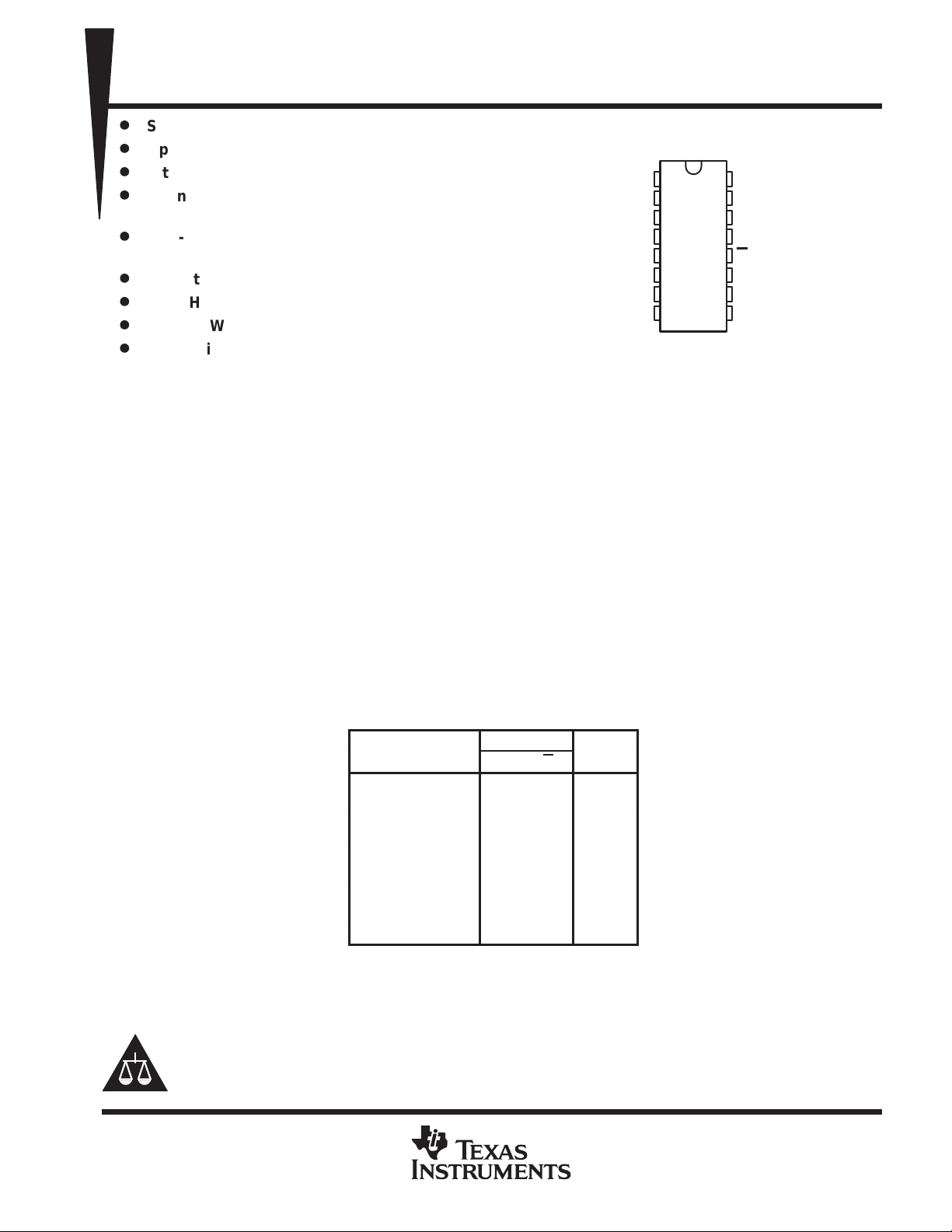
D OR NS† PACKAGE
(TOP VIEW)
16
1
1B
2
1A
3
1Y
4
G
5
2Y
6
2A
7
2B
GND
†
The NS package is only available
left-ended taped and reeled.
8
15
14
13
12
11
10
V
CC
4B
4A
4Y
G
3Y
3A
9
3B
description
The AM26L V32, BiCMOS, quadruple, differential line receiver with 3-state outputs is designed to be similar to
TIA/EIA-422-B and ITU Recommendation V.11 receivers with reduced common-mode voltage range due to
reduced supply voltage.
The device is optimized for balanced bus transmission at switching rates up to 32 MHz. The enable function
is common to all four receivers and offers a choice of active-high or active-low inputs. The 3-state outputs permit
connection directly to a bus-organized system. Each device features receiver high input impedance and input
hysteresis for increased noise immunity , and input sensitivity of ±200 mV over a common-mode input voltage
range from –0.3 V to 5.5 V . When the inputs are open circuited, the outputs are in the high logic state. This device
is designed using the Texas Instruments (TI) proprietary LinIMPACT-C60 technology, facilitating ultra-low
power consumption without sacrificing speed.
This device offers optimum performance when used with the AM26LV31 quadruple line drivers.
The AM26LV32C is characterized for operation from 0°C to 70°C.
FUNCTION TABLE
(each receiver)
DIFFERENTIAL
INPUT
VID ≥ 0.2 V
–0.2 V < VID < 0.2 V
VID ≤ –0.2 V
Open, shorted, or
terminated
H = high level, L = low level, X = irrelevant,
Z = high impedance (off), ? = indeterminate
‡
See application information attached.
Please be aware that an important notice concerning availability, standard warranty, and use in critical applications of
Texas Instruments semiconductor products and disclaimers thereto appears at the end of this data sheet.
‡
X L H Z
ENABLES
G G
H
X
H
X
H
X
H
X
X
L
X
L
X
L
X
L
H
H
?
?
L
L
H
H
LinIMP ACT-C60 and TI are trademarks of Texas Instruments.
PRODUCTION DATA information is current as of publication date.
Products conform to specifications per the terms of Texas Instruments
standard warranty. Production processing does not necessarily include
testing of all parameters.
POST OFFICE BOX 655303 • DALLAS, TEXAS 75265
Copyright 2000, Texas Instruments Incorporated
1
AM26LV32
LOW-VOLTAGE HIGH-SPEED
QUADRUPLE DIFFERENTIAL LINE RECEIVER
SLLS202D – MAY 1995 – REVISED APRIL 2000
1A
1B
2A
2B
3A
3B
4A
4B
†
4
G
12
G
2
1
6
7
10
9
14
15
≥ 1
EN
11
13
3
1Y
5
2Y
3Y
4Y
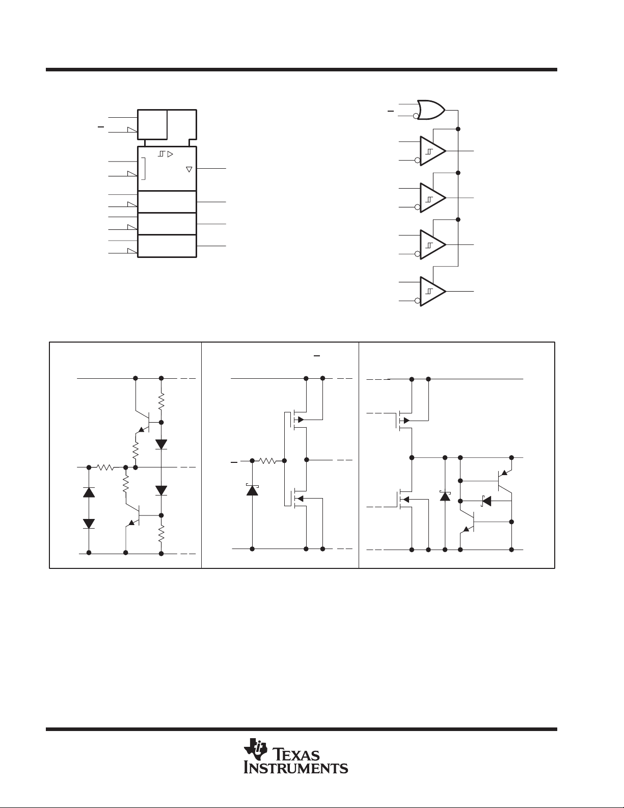
logic symbol
†
This symbol is in accordance with ANSI/IEEE Std 91-1984
and IEC Publication 617-12.
schematics of equivalent inputs and outputs
EQUIVALENT OF EACH INPUT (A, B)
V
CC
EQUIVALENT OF EACH
ENABLE INPUT (G, G
V
CC
logic diagram (positive logic)
4
G
12
G
2
1A
1
1B
6
2A
7
2B
10
3A
9
3B
14
4A
15
4B
)
TYPICAL OF ALL OUTPUTS (Y)
11
13
3
1Y
5
2Y
3Y
4Y
V
CC
A, B
GND
1.5 kΩ
15 kΩ
1.5 kΩ
7.2 kΩ
7.2 kΩ
Enable
G, G
GND
100 Ω
Y
GND
2
POST OFFICE BOX 655303 • DALLAS, TEXAS 75265

AM26LV32
LOW-VOLTAGE HIGH-SPEED
QUADRUPLE DIFFERENTIAL LINE RECEIVER
SLLS202D – MAY 1995 – REVISED APRIL 2000
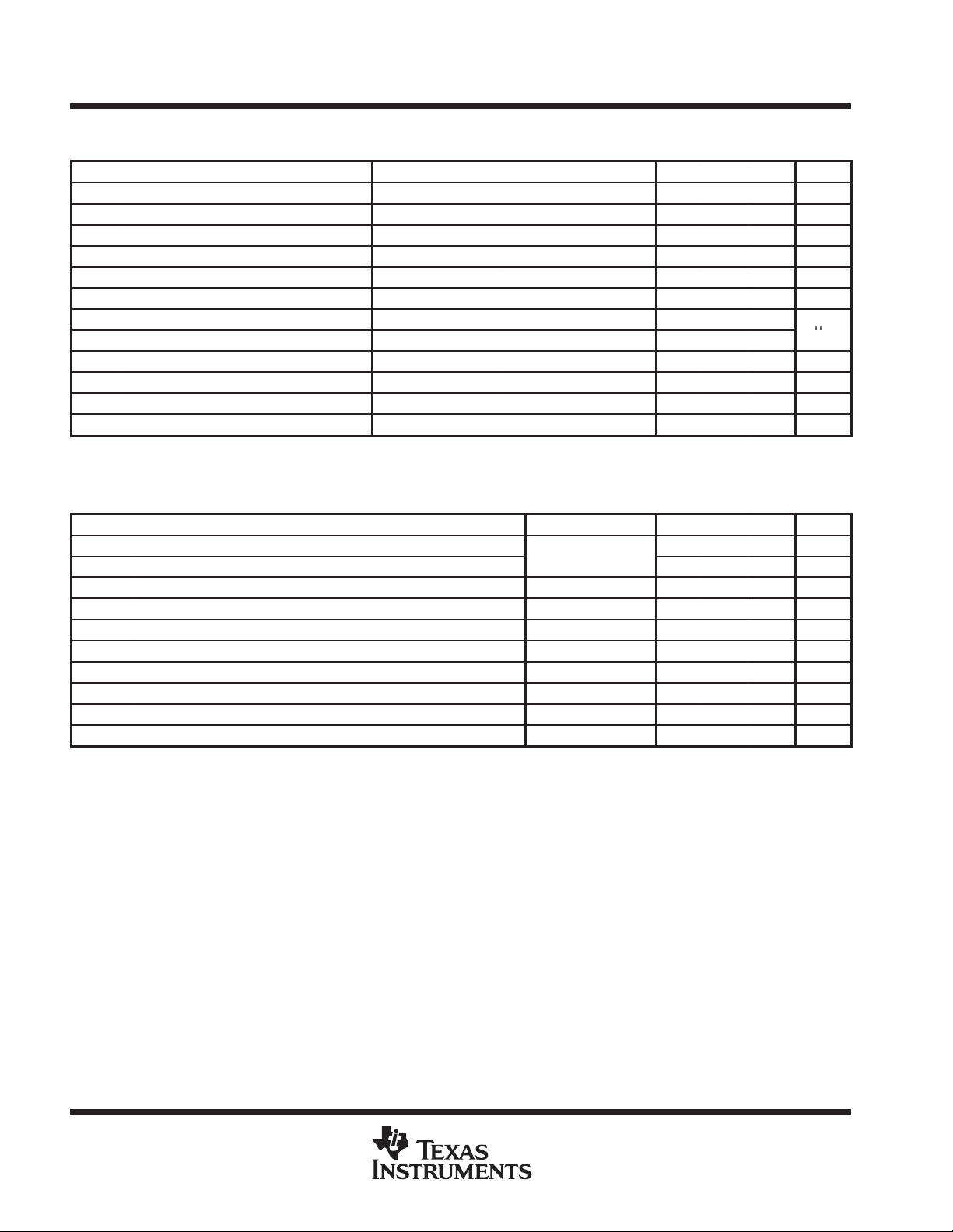
absolute maximum ratings over operating free-air temperature range (unless otherwise noted)
Supply voltage range, VCC (see Note 1) –0.3 V to 6 V. . . . . . . . . . . . . . . . . . . . . . . . . . . . . . . . . . . . . . . . . . . . . .
Input voltage range, VI (A or B inputs) –4 V to 8 V. . . . . . . . . . . . . . . . . . . . . . . . . . . . . . . . . . . . . . . . . . . . . . . . . .
Differential input voltage, V
(see Note 2) ±12 V. . . . . . . . . . . . . . . . . . . . . . . . . . . . . . . . . . . . . . . . . . . . . . . . . . .
ID
Enable input voltage range –0.3 V to 6 V. . . . . . . . . . . . . . . . . . . . . . . . . . . . . . . . . . . . . . . . . . . . . . . . . . . . . . . . . .
Output voltage range, VO –0.3 V to 6 V. . . . . . . . . . . . . . . . . . . . . . . . . . . . . . . . . . . . . . . . . . . . . . . . . . . . . . . . . . .
Maximum output current, IO ±25 mA. . . . . . . . . . . . . . . . . . . . . . . . . . . . . . . . . . . . . . . . . . . . . . . . . . . . . . . . . . . . . .
Package thermal impedance, θ
(see Note 3): D package 73°C/W. . . . . . . . . . . . . . . . . . . . . . . . . . . . . . . . . .
JA
NS package 64°C/W. . . . . . . . . . . . . . . . . . . . . . . . . . . . . . . . .
Lead temperature 1,6 mm (1/16 inch) from case for 10 seconds 260°C. . . . . . . . . . . . . . . . . . . . . . . . . . . . . . .
Storage temperature range, T
†
Stresses beyond those listed under “absolute maximum ratings” may cause permanent damage to the device. These are stress ratings only, and
functional operation of the device at these or any other conditions beyond those indicated under “recommended operating conditions” is not
implied. Exposure to absolute-maximum-rated conditions for extended periods may affect device reliability.
NOTES: 1. All voltage values are with respect to the GND terminal.
2. Differential input voltage is measured at the noninverting input with respect to the corresponding inverting input.
3. The package thermal impedance is calculated in accordance with JESD 51.
–65°C to 150°C. . . . . . . . . . . . . . . . . . . . . . . . . . . . . . . . . . . . . . . . . . . . . . . . . . .
stg
recommended operating conditions
MIN NOM MAX UNIT
Supply voltage, V
High-level input voltage, V
Low-level input voltage, V
Common-mode input voltage, V
Differential input voltage, V
High-level output current, I
Low-level output current, I
Operating free-air temperature, T
CC
IH(EN)
IL(EN)
ID
OH
OL
IC
A
AM26LV32C 0 70 °C
3 3.3 3.6 V
2 V
0.8 V
–0.3 5.5 V
±5.8
–5 mA
5 mA
†
POST OFFICE BOX 655303 • DALLAS, TEXAS 75265
3
AM26LV32
A
See Figure 1
LOW-VOLTAGE HIGH-SPEED
QUADRUPLE DIFFERENTIAL LINE RECEIVER
SLLS202D – MAY 1995 – REVISED APRIL 2000
electrical characteristics over recommended supply-voltage and operating free-air temperature
ranges (unless otherwise noted)
PARAMETER TEST CONDITIONS MIN TYP†MAX UNIT
V
V
V
V
V
I
I
I
r
I
I
C
†
‡
Differential input high-threshold voltage 0.2 V
IT+
Differential input low-threshold voltage –0.2 V
IT–
Enable input clamp voltage II = –18 mA –0.8 –1.5 V
IK
High-level output voltage VID = 200 mV, IOH = –5 mA 2.4 3.2 V
OH
Low-level output voltage VID = –200 mV, IOL = 5 mA 0.17 0.5 V
OL
High-impedance-state output current VO = 0 to V
OZ
High-level enable input current VCC = 0 or 3 V, VI = 5.5 V 10
IH(E)
Low-level enable input current VCC = 3.6 V, VI = 0 V –10
IL(E)
Input resistance 7 12 kΩ
I
Input current VI = 5.5 V or –0.3 V, All other inputs GND ±700 µA
I
Supply current V
CC
Power dissipation capacitance
pd
All typical values are at VCC = 3.3 V and TA = 25°C.
Cpd determines the no-load dynamic current: IS = Cpd × VCC × f + ICC.
‡
I(E)
One channel 150 pF
CC
= VCC or GND, No load, line inputs open 8 17 mA
±50 µA
µ
switching characteristics, VCC = 3.3 V, TA = 25°C
PARAMETER TEST CONDITIONS MIN TYP MAX UNIT
t
PLH
t
PHL
t
t
t
PZH
t
PZL
t
PHZ
t
PLZ
t
sk(p)
t
sk(o)
t
sk(pp)
§
t
¶
t
#
t
sk(p)
sk(o)
sk(pp)
Propagation delay time, low- to high-level output
Propagation delay time, high- to low-level output
Transistion time (tr or tf) See Figure 1 5 ns
Output-enable time to high level See Figure 2 17 40 ns
Output-enable time to low level See Figure 3 10 40 ns
Output-disable time from high level See Figure 2 20 40 ns
Output-disable time from low level See Figure 3 16 40 ns
§
Pulse skew 4 6 ns
¶
Pulse skew 4 6 ns
#
Pulse skew (device to device) 6 9 ns
is |t
is the maximum difference in propagation delay times between any two channels of the same device switching in the same direction.
– t
PLH
is the maximum difference in propagation delay times between any two channels of any two devices switching in the same direction.
| of each channel of the same device.
PHL
8 16 20 ns
8 16 20 ns
4
POST OFFICE BOX 655303 • DALLAS, TEXAS 75265
AM26LV32
LOW-VOLTAGE HIGH-SPEED
QUADRUPLE DIFFERENTIAL LINE RECEIVER
SLLS202D – MAY 1995 – REVISED APRIL 2000
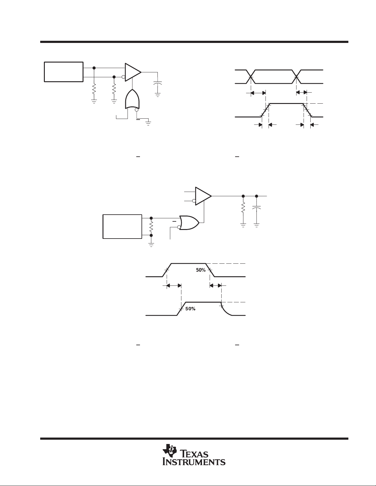
PARAMETER MEASUREMENT INFORMATION
Generator
(see Note B)
NOTES: A. CL includes probe and jig capacitance.
B. The input pulse is supplied by a generator having the following characteristics: ZO = 50 Ω, PRR = 10 MHz, tr and tf (10% to 90%)
≤ 2 ns, 50% duty cycle.
C. To test the active-low enable G
A
B
50 Ω50 Ω
V
CC
Figure 1. t
Generator
(see Note B)
GG
(see Note C)
, ground G and apply an inverted waveform G.
PLH
Y
and t
V
O
CL = 15 pF
(see Note A)
PHL
VID = 1 V
50 Ω
A
Input
B
t
PLH
Output
50% 50%
10% 10%
t
r
Test Circuit and Voltage Waveforms
A
B
G
G
Y
RL = 2 kΩ
CL = 15 pF
(see Note A)
90% 90%
V
O
t
PHL
2 V
1 V
V
OH
V
OL
t
f
Input
t
PZH
Output
NOTES: A. CL includes probe and jig capacitance.
B. The input pulse is supplied by a generator having the following characteristics: ZO = 50 Ω, PRR = 10 MHz, tr and tf (10% to 90%)
≤ 2 ns, 50% duty cycle.
C. To test the active-low enable G
Figure 2. t
, ground G and apply an inverted waveform G.
and t
PZH
V
CC
(see Note C)
50%
Test Circuit and Voltage Waveforms
PHZ
50%
50%
t
PHZ
VOH – 0.3 V
V
0 V
V
V
CC
OH
off
≈ 0
POST OFFICE BOX 655303 • DALLAS, TEXAS 75265
5

AM26LV32
LOW-VOLTAGE HIGH-SPEED
QUADRUPLE DIFFERENTIAL LINE RECEIVER
SLLS202D – MAY 1995 – REVISED APRIL 2000
PARAMETER MEASUREMENT INFORMATION
A
B
G
G
V
CC
50%
Generator
(see Note B)
Input
VID = 1 V
50 Ω
(see Note C)
t
PZL
50%
V
CC
RL = 2 kΩ
Y
t
PLZ
V
O
CL = 15 pF
(see Note A)
V
CC
0 V
Output
NOTES: A. CL includes probe and jig capacitance.
B. The input pulse is supplied by a generator having the following characteristics: ZO = 50 Ω, PRR = 10 MHz, tr and tf (10% to 90%)
≤ 2 ns, 50% duty cycle.
C. To test the active-low enable G, ground G and apply an inverted waveform G.
Figure 3. t
PZL
and t
V
50%
Test Circuit and Voltage Waveforms
PLZ
VOL + 0.3 V
off
V
OL
≈ V
CC
6
POST OFFICE BOX 655303 • DALLAS, TEXAS 75265

AM26LV32
LOW-VOLTAGE HIGH-SPEED
QUADRUPLE DIFFERENTIAL LINE RECEIVER
SLLS202D – MAY 1995 – REVISED APRIL 2000
APPLICATION INFORMATION
fail-safe conditions
The AM26LV32 quadruple differential line receiver is designed to function properly when appropriately
connected to active drivers. Applications do not always have ideal situations where all bits are being used, the
receiver inputs are never left floating, and fault conditions don’t exist. In actuality, most applications have the
capability to either place the drivers in a high-impedance mode or power down the drivers altogether, and cables
may be purposely (or inadvertently) disconnected, both of which lead to floating receiver inputs. Furthermore,
even though measures are taken to avoid fault conditions like a short between the differential signals, this does
occur. The AM26LV32 has an internal fail-safe circuitry which prevents the device from putting an unknown
voltage signal at the receiver outputs. In the following three cases, a high-state is produced at the respective
output:
1. Open fail-safe – Unused input pins are left open. Do not tie unused pins to ground or any other
voltage. Internal circuitry places the output in the high state.
2. 100-ohm terminated fail-safe – Disconnected cables, drivers in high-impedance state, or
powered-down drivers will not cause the AM26L V32 to malfunction. The outputs will remain in
a high state under these conditions. When the drivers are either turned-off or placed into the
high-impedance state, the receiver input may still be able to pick up noise due to the cable acting
as an antenna. To avoid having a large differential voltage being generated, the use of
twisted-pair cable will induce the noise as a common-mode signal and will be rejected.
3. Shorted fail-safe – Fault conditions that short the differential input pairs together will not cause
incorrect data at the outputs. A differential voltage (V
outputs. Shorted fail-safe, however, is not supported across the recommended common-mode
input voltage (VIC) range. An unwanted state can be induced to all outputs when an input is
shorted and is biased with a voltage between –0.3 V and 5.5 V. The shorted fail-safe circuitry
will function properly when an input is shorted, but with no external common-mode voltage
applied.
) of 0 V will force a high state at the
ID
fail-safe precautions
The internal fail-safe circuitry was designed such that the input common-mode (VIC) and differential
(VID)voltages must be observed. In order to ensure the outputs of unused or inactive receivers remain in a high
state when the inputs are open-circuited, shorted, or terminated, extra precaution must be taken on the active
signal. In applications where the drivers are placed in a high-impedance mode or are powered-down, it is
recommended that for 1, 2, or 3 active receiver inputs, the low-level input voltage (V
0.4 V . As in all data transmission applications, it is necessary to provide a return ground path between the two
remote grounds (driver and receiver ground references) to avoid ground differences. Table 1 and Figures 4
through 7 are examples of active input voltages with their respective waveforms and the effect each have on
unused or inactive outputs. Note that the active receivers behave as expected, regardless of the input levels.
) should be greater than
IL
POST OFFICE BOX 655303 • DALLAS, TEXAS 75265
7

AM26LV32
FIGURE
ACTIVE OUTPUTS
LOW-VOLTAGE HIGH-SPEED
QUADRUPLE DIFFERENTIAL LINE RECEIVER
SLLS202D – MAY 1995 – REVISED APRIL 2000
APPLICATION INFORMATION
Table 1. Active Receiver Inputs vs Outputs
VIL = 900 mV
1, 2, OR 3
ACTIVE INPUTS
†
V
IL
900 mV 200 mV 1 V 4 Known state High state
–100 mV 200 mV 0 V 5 Known state ?
600 mV 800 mV 1 V 6 Known state High state
0 800 mV 400 mV 7 Known state ?
†
Measured with respect to ground.
V
VIC = 1V
ID
VID = 200 mV
†
V
IC
0V
SEE
1, 2, OR 3
Produces a High State at
Unused or Inactive Outputs
Figure 4. Waveform One
An Unknown State is Produced
at Unused or Inactive Outputs
VIL = –100 mV
VIC = 0V
VID = 200 mV
Figure 5. Waveform Two
3, 2, OR 1 UNUSED
OR INACTIVE
OUTPUTS
VIL = 600 mV
VIL = 0V
8
VIC = 1V
VIC = 400 mV
VID = 800 mV
0V
Figure 6. Waveform Three
VID = 800 mV
0V
Figure 7. Waveform Four
POST OFFICE BOX 655303 • DALLAS, TEXAS 75265
Produces a High State at
Unused or Inactive Outputs
An Unknown State is Produced
at Unused or Inactive Outputs

AM26LV32
LOW-VOLTAGE HIGH-SPEED
QUADRUPLE DIFFERENTIAL LINE RECEIVER
SLLS202D – MAY 1995 – REVISED APRIL 2000
APPLICATION INFORMATION
In most applications, it is not customary to have a common-mode input close to ground and to have a differential
voltage larger than 2 V . Since the common-mode input voltage is typically around 1.5 V, a 2-V VID would result
in a V
Figure 8 plots seven different input threshold curves from a variety of production lots and shows how the fail-safe
circuitry behaves with the input common-mode voltage levels. These input threshold curves are representative
samples of production devices. The curves specifically illustrate a typical range of input threshold variation. The
AM26L V32 is specified with ±200 mV of input sensitivity to account for the variance in input threshold. Each data
point represents the input’s ability to produce a known state at the output for a given VIC and VID. Applying a
differential voltage at or above a certain point on a curve would produce a known state at the output. Applying
a differential voltage less than a certain point on a curve would activate the fail-safe circuit and the output would
be in a high state. For example, inspecting the top input threshold curve reveals that for a V
around 87 mV . Applying 90 mV of differential voltage to this particular production lot generates a known receiver
output voltage. Applying a VID of 80 mV activates the input fail-safe circuitry and the receiver output is placed
in the high state. Texas Instruments specifies the input threshold at ±200 mV, since normal process variations
affect this parameter . Note that at common-mode input voltages around 0.2 V , the input differential voltages are
low compared to their respective data points. This phenomenon points to the fact that the inputs are very
sensitive to small differential voltages around 0.2 V V
0.5 V to avoid this increased sensitivity at VIC [ 0.2 V. In most applications, since VIC typically is 1.5 V, the
fail-safe circuitry functions properly to provide a high state at the receiver output.
of 0.5 V, thus satisfying the recommended VIL level of greater than 0.4 V.
IL
. It is recommended that VIC levels be kept greater than
IC
+ 1.6 V , VID yields
IC
Most
Applications
100
90
80
70
60
Not
50
40
Differential Voltage – mV–
30
ID
V
20
10
0
–0.8 –0.6 –0.4 –0.2 0 0.2 0.4 0.6 0.8 1 1.2 1.4 1.6 1.8 2 2.2 2.4–1
Recommended
Increased Receiver Input Sensitivity
VIC – Common-Mode Input Voltage – V
Figure 8. VIC Versus VID Receiver Sensitivity Levels
POST OFFICE BOX 655303 • DALLAS, TEXAS 75265
9

AM26LV32
LOW-VOLTAGE HIGH-SPEED
QUADRUPLE DIFFERENTIAL LINE RECEIVER
SLLS202D – MAY 1995 – REVISED APRIL 2000
APPLICATION INFORMATION
Figure 9 represents a typical application where two receivers are not used. In this case, there is no need to worry
about the output voltages of the unused receivers since they are not connected in the system architecture.
Connector
Unused Circuit
R
T
R
T
AM26LV32
System
Figure 9. Typical Application with Unused Receivers
Figure 10 shows a common application where one or more drivers are either disabled or powered down. To
ensure the inactive receiver outputs are in a high state, the active receiver inputs must have V
> 0.4 V and V
IL
IC
0.5 V.
Enable
Disable or
Power Off
Driver
Connector
Cable
Connector
R
T
R
T
R
T
R
T
AM26LV32
System
>
10
Figure 10. Typical Application Where Two or More Drivers are Disabled
POST OFFICE BOX 655303 • DALLAS, TEXAS 75265

AM26LV32
LOW-VOLTAGE HIGH-SPEED
QUADRUPLE DIFFERENTIAL LINE RECEIVER
SLLS202D – MAY 1995 – REVISED APRIL 2000
APPLICATION INFORMATION
Figure 11 is an alternative application design to replace the application in Figure 10. This design uses two
AM26LV32 devices, instead of one. However, this design does not require the input levels be monitored to
ensure the outputs are in the correct state, only that they comply to the RS-232 standard.
Enable
Disable or
Power Off
Driver
Connector
Cable
Connector
Unused Circuit
R
T
R
T
AM26LV32
System
R
T
R
T
Unused Circuit
Figure 11. Alternative Solution for Figure 10
AM26LV32
POST OFFICE BOX 655303 • DALLAS, TEXAS 75265
11

AM26LV32
LOW-VOLTAGE HIGH-SPEED
QUADRUPLE DIFFERENTIAL LINE RECEIVER
SLLS202D – MAY 1995 – REVISED APRIL 2000
APPLICATION INFORMATION
Figures 12 and 13 show typical applications where a disconnected cable occurs. Figure 12 illustrates a typical
application where a cable is disconnected. Similar to Figure 10, the active input levels must be monitored to
make sure the inactive receiver outputs are in a high state. An alternative solution is shown in Figure 13.
Driver
Connector
Cable
Connector
R
T
R
T
AM26LV32
System
Unplugged
Cable
R
T
R
T
Figure 12. Typical Application Where Two or More Drivers are Disconnected
12
POST OFFICE BOX 655303 • DALLAS, TEXAS 75265

AM26LV32
LOW-VOLTAGE HIGH-SPEED
QUADRUPLE DIFFERENTIAL LINE RECEIVER
SLLS202D – MAY 1995 – REVISED APRIL 2000
APPLICATION INFORMATION
Figure 13 is an alternative solution so the receiver inputs do not have to be monitored. This solution also requires
the use of two AM26LV32 devices, instead of one.
Driver
Connector
Cable
Connector
Unused Circuit
R
T
R
T
AM26LV32
System
Unplugged
Cable
R
T
R
T
Unused Circuit
AM26LV32
Figure 13. Alternative Solution to Figure 12
POST OFFICE BOX 655303 • DALLAS, TEXAS 75265
13

AM26LV32
LOW-VOLTAGE HIGH-SPEED
QUADRUPLE DIFFERENTIAL LINE RECEIVER
SLLS202D – MAY 1995 – REVISED APRIL 2000
APPLICATION INFORMATION
When designing a system using the AM26L V32, the device provides a robust solution where fail-safe and fault
conditions are of concern. The RS-422-like inputs accept common-mode input levels from –0.3 V to 5.5 V with
a specified sensitivity of ±200mV. As previously shown, care must be taken with active input levels since they
can affect the outputs of unused or inactive bits. However , most applications meet or exceed the requirements
to allow the device to perform properly.
14
POST OFFICE BOX 655303 • DALLAS, TEXAS 75265

IMPORTANT NOTICE
T exas Instruments and its subsidiaries (TI) reserve the right to make changes to their products or to discontinue
any product or service without notice, and advise customers to obtain the latest version of relevant information
to verify, before placing orders, that information being relied on is current and complete. All products are sold
subject to the terms and conditions of sale supplied at the time of order acknowledgment, including those
pertaining to warranty, patent infringement, and limitation of liability.
TI warrants performance of its semiconductor products to the specifications applicable at the time of sale in
accordance with TI’s standard warranty. Testing and other quality control techniques are utilized to the extent
TI deems necessary to support this warranty . Specific testing of all parameters of each device is not necessarily
performed, except those mandated by government requirements.
Customers are responsible for their applications using TI components.
In order to minimize risks associated with the customer’s applications, adequate design and operating
safeguards must be provided by the customer to minimize inherent or procedural hazards.
TI assumes no liability for applications assistance or customer product design. TI does not warrant or represent
that any license, either express or implied, is granted under any patent right, copyright, mask work right, or other
intellectual property right of TI covering or relating to any combination, machine, or process in which such
semiconductor products or services might be or are used. TI’s publication of information regarding any third
party’s products or services does not constitute TI’s approval, warranty or endorsement thereof.
Copyright 2000, Texas Instruments Incorporated
 Loading...