

AM26LS31C
QUADRUPLE DIFFERENTIAL LINE DRIVER
SLLS114D – JANUARY 1979 – REVISED OCT OBER 1998
1
POST OFFICE BOX 655303 • DALLAS, TEXAS 75265
D
Meets or Exceeds the Requirements of
ANSI TIA/EIA-422-B and ITU
Recommendation V.1 1
D
Operates From a Single 5-V Supply
D
TTL Compatible
D
Complementary Outputs
D
High Output Impedance in Power-Off
Conditions
D
Complementary Output-Enable Inputs
description
The AM26LS31C is a quadruple complementary-output line driver designed to meet the requirements of
ANSI TIA/EIA-422-B and ITU (formerly CCITT) Recommendation V .11. The 3-state outputs have high-current
capability for driving balanced lines such as twisted-pair or parallel-wire transmission lines, and they provide
a high-impedance state in the power-off condition. The enable function is common to all four drivers and offers
the choice of an active-high or active-low enable (G, G
) input. Low-power Schottky circuitry reduces power
consumption without sacrificing speed.
The AM26LS31C is characterized for operation from 0°C to 70°C.
FUNCTION TABLE
(each driver)
INPUT
ENABLES OUTPUTS
A
G G Y Z
H H X H L
L H XLH
H XLHL
L XLLH
X LHZZ
H = high level, L = low level, X = irrelevant,
Z = high impedance (off)
Copyright 1998, Texas Instruments Incorporated
PRODUCTION DATA information is current as of publication date.
Products conform to specifications per the terms of Texas Instruments
standard warranty. Production processing does not necessarily include
testing of all parameters.
Please be aware that an important notice concerning availability, standard warranty, and use in critical applications of
Texas Instruments semiconductor products and disclaimers thereto appears at the end of this data sheet.
1
2
3
4
5
6
7
8
16
15
14
13
12
11
10
9
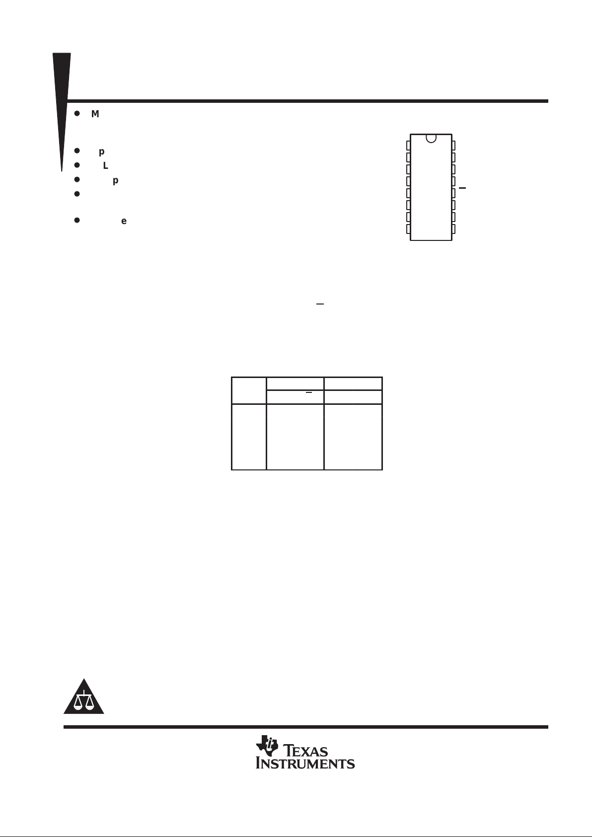
1A
1Y
1Z
G
2Z
2Y
2A
GND
V
CC
4A
4Y
4Z
G
3Z
3Y
3A
D OR N PACKAGE
(TOP VIEW)
AM26LS31C
QUADRUPLE DIFFERENTIAL LINE DRIVER
SLLS114D – JANUARY 1979 – REVISED OCT OBER 1998
2
POST OFFICE BOX 655303 • DALLAS, TEXAS 75265
logic symbol
†
4
G
12
1Y
2
1Z
3
1
1A
≥1
EN
2Y
6
2Z
5
7
2A
3Y
10
3Z
11
9
3A
4Y
14
4Z
13
15
4A
G
logic diagram (positive logic)
1Z
1Y
G
G
1A
4
12
1
2
3
2Z
2Y
2A
7
6
5
3Z
3Y
3A
9
10
11
4Z
4Y
4A
15
14
13
AM26LS31C
QUADRUPLE DIFFERENTIAL LINE DRIVER
SLLS114D – JANUARY 1979 – REVISED OCT OBER 1998
3
POST OFFICE BOX 655303 • DALLAS, TEXAS 75265
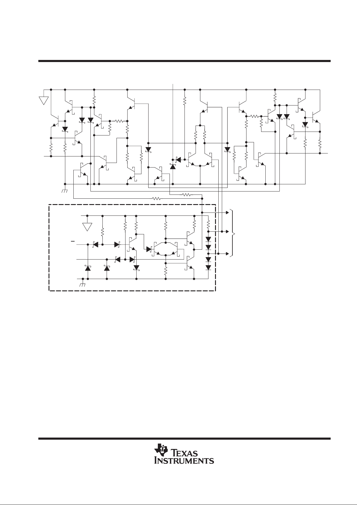
schematic (each driver)
22 kΩ
To Three Other Drivers
Common to All Four Drivers
GND
Enable G
Enable G
V
CC
V
V
Output Y
9 Ω
Input A
22 kΩ
22 kΩ
All resistor values are nominal.
Output Z
9 Ω
absolute maximum ratings over operating free-air temperature range (unless otherwise noted)
†
Supply voltage, V
CC
(see Note 1) 7 V. . . . . . . . . . . . . . . . . . . . . . . . . . . . . . . . . . . . . . . . . . . . . . . . . . . . . . . . . . . . .
Input voltage, V
I
7 V. . . . . . . . . . . . . . . . . . . . . . . . . . . . . . . . . . . . . . . . . . . . . . . . . . . . . . . . . . . . . . . . . . . . . . . . . . . .
Output off-state voltage 5.5 V. . . . . . . . . . . . . . . . . . . . . . . . . . . . . . . . . . . . . . . . . . . . . . . . . . . . . . . . . . . . . . . . . . . .
Package thermal impedance, θ
JA
(see Note 2): D package 113°C/W. . . . . . . . . . . . . . . . . . . . . . . . . . . . . . . . . .
N package 78°C/W. . . . . . . . . . . . . . . . . . . . . . . . . . . . . . . . . . .
Storage temperature range, T
stg
–65°C to 150°C. . . . . . . . . . . . . . . . . . . . . . . . . . . . . . . . . . . . . . . . . . . . . . . . . . .
Lead temperature 1,6 mm (1/16 inch) from case for 10 seconds 260°C. . . . . . . . . . . . . . . . . . . . . . . . . . . . . . .
†
Stresses beyond those listed under “absolute maximum ratings” may cause permanent damage to the device. These are stress ratings only, and
functional operation of the device at these or any other conditions beyond those indicated under “recommended operating conditions” is not
implied. Exposure to absolute-maximum-rated conditions for extended periods may affect device reliability.
NOTES: 1. All voltage values, except differential output voltage VOD, are with respect to network GND.
2. The package thermal impedance is calculated in accordance with JESD 51, except for through-hole packages, which use a trace
length of zero.

AM26LS31C
QUADRUPLE DIFFERENTIAL LINE DRIVER
SLLS114D – JANUARY 1979 – REVISED OCT OBER 1998
4
POST OFFICE BOX 655303 • DALLAS, TEXAS 75265
recommended operating conditions (unless otherwise noted)
MIN NOM MAX UNIT
Supply voltage, V
CC
4.75 5 5.25 V
High-level input voltage, V
IH
2 V
Low-level input voltage, V
IL
0.8 V
High-level output current, I
OH
–20 mA
Low-level output current, I
OL
20 mA
Operating free-air temperature, T
A
0 70 °C
electrical characteristics over operating free-air temperature range (unless otherwise noted)
PARAMETER TEST CONDITIONS MIN TYP†MAX UNIT
V
IK
Input clamp voltage VCC = 4.75 V , II = –18 mA –1.5 V
V
OH
High-level output voltage VCC = 4.75 V , IOH = –20 mA 2.5 V
V
OL
Low-level output voltage VCC = 4.75 V , IOL = 20 mA 0.5 V
p
p
VO = 0.5 V –20
IOZOff-state (high-impedance-state) output current
V
CC
=
4.75 V
VO = 2.5 V 20
µ
A
I
I
Input current at maximum input voltage VCC = 5.25 V , VI = 7 V 0.1 mA
I
IH
High-level input current VCC = 5.25 V , VI = 2.7 V 20 µA
I
IL
Low-level input current VCC = 5.25 V , VI = 0.4 V –0.36 mA
I
OS
Short-circuit output current
‡
VCC = 5.25 V –30 –150 mA
I
CC
Supply current VCC = 5.25 V , All outputs disabled 32 80 mA
†
All typical values are at VCC = 5 V and TA = 25°C.
‡
Not more than one output should be shorted at a time, and duration of the short circuit should not exceed one second.
switching characteristics, VCC = 5 V, TA = 25°C (see Figure 1)
PARAMETER TEST CONDITIONS MIN TYP MAX UNIT
t
PLH
Propagation delay time, low-to-high-level output
p
p
14 20
t
PHL
Propagation delay time, high-to-low-level output
C
L
= 30 pF,
S1 and S2 open
14 20
ns
t
PZH
Output enable time to high level
p
RL = 75 Ω 25 40
t
PZL
Output enable time to low level
C
L
= 30
pF
RL = 180 Ω 37 45
ns
t
PHZ
Output disable time from high level
p
21 30
t
PLZ
Output disable time from low level
C
L
=
10 pF
,
S1 and S2 closed
23 35
ns
Output-to-output skew CL = 30 pF, S1 and S2 open 1 6 ns

AM26LS31C
QUADRUPLE DIFFERENTIAL LINE DRIVER
SLLS114D – JANUARY 1979 – REVISED OCT OBER 1998
5
POST OFFICE BOX 655303 • DALLAS, TEXAS 75265
PARAMETER MEASUREMENT INFORMATION
Waveform 1
(see Note E)
Output Z
Output Y
Input A
(see Notes B
and C)
V
OL
V
OH
V
OL
V
OH
3 V
t
PHL
Skew Skew
t
PLH
t
PLH
t
PHL
0 V
PROPAGATION DELAY TIMES AND SKEW TEST CIRCUIT
V
CC
Test Point
S1
S2
75 Ω
180 Ω
C
L
(see Note A)
From Output
Under Test
V
OH
V
OL
≈1.5 V
0 V
3 V
Enable G
Enable G
(see Note D)
S1 Open
S2 Closed
S1 Closed
S2 Open
t
PZH
t
PZL
t
PHZ
t
PLZ
S1 Closed
S2 Closed
0.5 V
≈0 V
≈4.5 V
S1 Closed
S2 Closed
≈1.5 V
ENABLE AND DISABLE TIME WAVEFORMS
See Note D
NOTES: A. CL includes probe and jig capacitance.
B. All input pulses are supplied by generators having the following characteristics: PRR ≤ 1 MHz, ZO ≈ 50 Ω, tr ≤ 15 ns, tf ≤ 6 ns.
C. When measuring propagation delay times and skew, switches S1 and S2 are open.
D. Each enable is tested separately.
E. Waveform 1 is for an output with internal conditions such that the output is low except when disabled by the output control.
Waveform 2 is for an output with internal conditions such that the output is high except when disabled by the output control.
1.3 V 1.3 V
1.5 V
1.5 V
1.5 V 1.5 V
Waveform 2
(see Note E)
0.5 V
1.5 V
1.5 V
Figure 1. Test Circuit and V oltage Waveforms

AM26LS31C
QUADRUPLE DIFFERENTIAL LINE DRIVER
SLLS114D – JANUARY 1979 – REVISED OCT OBER 1998
6
POST OFFICE BOX 655303 • DALLAS, TEXAS 75265
TYPICAL CHARACTERISTICS
Figure 2
VI – Enable G Input Voltage – V
OUTPUT VOLTAGE
vs
ENABLE G INPUT VOLTAGE
VCC = 5.25 V
VCC = 5 V
VCC = 4.75 V
Load = 470 Ω to GND
TA = 25°C
See Note A
– Y Output Voltage – V
V
O
4
3
2
1
0
0123
Figure 3
VI – Enable G Input Voltage – V
OUTPUT VOLTAGE
vs
ENABLE G INPUT VOLTAGE
VCC = 5 V
Load = 470 Ω to GND
See Note A
ÎÎÎÎ
TA = 70°C
TA = 0°C
TA = 25°C
– Y Output Voltage – VV
O
4
3
2
1
0
0123
Figure 4
VI – Enable G Input Voltage – V
– Output Voltage – V
OUTPUT VOLTAGE
vs
ENABLE G INPUT VOLTAGE
V
O
VCC = 5.25 V
VCC = 5 V
VCC = 4.75 V
4
3
2
1
0
0123
5
6
Load = 470 Ω to V
CC
TA = 25°C
See Note B
Figure 5
VI – Enable G Input Voltage – V
OUTPUT VOLTAGE
vs
ENABLE G INPUT VOLTAGE
TA = 25°C
TA = 0°C
TA = 70°C
– Output Voltage – VV
O
4
3
2
1
0
0123
5
6
V
CC
= 5 V
Load = 470 Ω to V
CC
See Note B
NOTES: A. The A input is connected to VCC during testing of the Y outputs and to ground during testing of the Z outputs.
B. The A input is connected to ground during testing of the Y outputs and to VCC during testing of the Z outputs.

AM26LS31C
QUADRUPLE DIFFERENTIAL LINE DRIVER
SLLS114D – JANUARY 1979 – REVISED OCT OBER 1998
7
POST OFFICE BOX 655303 • DALLAS, TEXAS 75265
TYPICAL CHARACTERISTICS
Figure 6
– High-Level Output Voltage – V
TA – Free-Air Temperature –°C
IOH = –20 mA
IOH = –40 mA
HIGH-LEVEL OUTPUT VOLTAGE
vs
FREE-AIR TEMPERATURE
V
OH
VCC = 5 V
See Note A
4
3
2
1
0
0255075
5
Figure 7
IOH – High-Level Output Current – mA
HIGH-LEVEL OUTPUT VOLTAGE
vs
HIGH-LEVEL OUTPUT CURRENT
VCC = 5.25 V
VCC = 4.75 V
VCC = 5 V
TA = 25°C
See Note A
– High-Level Output Voltage – V
V
OH
4
3
2
1
0
0 –20
–40 –60 –80 –100
Figure 8
– Low-Level Output Voltage – V
TA – Free-Air Temperature – °C
VCC = 5 V
IOL = 40 mA
See Note B
LOW-LEVEL OUTPUT VOLTAGE
vs
FREE-AIR TEMPERATURE
V
OL
0.4
0.3
0.2
0.1
0
25 50 75
0.5
0
Figure 9
IOL – Low-Level Output Current – mA
LOW-LEVEL OUTPUT VOLTAGE
vs
LOW-LEVEL OUTPUT CURRENT
VCC = 5.25 V
VCC = 4.75 V
TA = 25°C
See Note B
– Low-Level Output Voltage – VV
OL
0.4
0.3
0.2
0.1
0
40 80 120
0.5
0 1006020
0.6
0.7
0.8
0.9
1
NOTES: A. The A input is connected to VCC during testing of the Y outputs and to ground during testing of the Z outputs.
B. The A input is connected to ground during testing of the Y outputs and to VCC during testing of the Z inputs.

AM26LS31C
QUADRUPLE DIFFERENTIAL LINE DRIVER
SLLS114D – JANUARY 1979 – REVISED OCT OBER 1998
8
POST OFFICE BOX 655303 • DALLAS, TEXAS 75265
TYPICAL CHARACTERISTICS
VCC = 5 V
Figure 10
VI – Data Input Voltage – V
Y OUTPUT VOLTAGE
vs
DATA INPUT VOLTAGE
VCC = 4.75 V
No Load
TA = 25°C
VCC = 5.25 V
– Y Output Voltage – V
V
O
4
3
2
1
0
0123
5
Figure 11
Y OUTPUT VOLTAGE
vs
DATA INPUT VOLTAGE
TA = 25°C
No Load
TA = 0°C
TA = 70°C
VI – Data Input Voltage – V
– Y Output Voltage – VV
O
4
3
2
1
0
0123
5

IMPORTANT NOTICE
T exas Instruments and its subsidiaries (TI) reserve the right to make changes to their products or to discontinue
any product or service without notice, and advise customers to obtain the latest version of relevant information
to verify, before placing orders, that information being relied on is current and complete. All products are sold
subject to the terms and conditions of sale supplied at the time of order acknowledgement, including those
pertaining to warranty, patent infringement, and limitation of liability.
TI warrants performance of its semiconductor products to the specifications applicable at the time of sale in
accordance with TI’s standard warranty. Testing and other quality control techniques are utilized to the extent
TI deems necessary to support this warranty. Specific testing of all parameters of each device is not necessarily
performed, except those mandated by government requirements.
CERT AIN APPLICATIONS USING SEMICONDUCTOR PRODUCTS MAY INVOLVE POTENTIAL RISKS OF
DEATH, PERSONAL INJURY, OR SEVERE PROPERTY OR ENVIRONMENTAL DAMAGE (“CRITICAL
APPLICATIONS”). TI SEMICONDUCTOR PRODUCTS ARE NOT DESIGNED, AUTHORIZED, OR
WARRANTED TO BE SUITABLE FOR USE IN LIFE-SUPPORT DEVICES OR SYSTEMS OR OTHER
CRITICAL APPLICATIONS. INCLUSION OF TI PRODUCTS IN SUCH APPLICA TIONS IS UNDERST OOD TO
BE FULLY AT THE CUSTOMER’S RISK.
In order to minimize risks associated with the customer’s applications, adequate design and operating
safeguards must be provided by the customer to minimize inherent or procedural hazards.
TI assumes no liability for applications assistance or customer product design. TI does not warrant or represent
that any license, either express or implied, is granted under any patent right, copyright, mask work right, or other
intellectual property right of TI covering or relating to any combination, machine, or process in which such
semiconductor products or services might be or are used. TI’s publication of information regarding any third
party’s products or services does not constitute TI’s approval, warranty or endorsement thereof.
Copyright 1998, Texas Instruments Incorporated
 Loading...